

SONIX SNC725 Datasheet

SNC725
1
16-bit Voice Processor
1. INTRODUCTION
SNC725 is a 16mins two-channel speech/melody and 4-channel wave-table melody
voice chip. It based on reduced 16-bit fixed-point DSP architecture. SNC725 provides
user some necessary and efficient DSP instructions. Furthermore, SNC725 provide one
10-bit PWM and one 10-bit DA converter to driving speaker for speech/melody output.
User can select PWM or DA by programming DA/PWM control register, and only one
function can be active at the same time.
2. FEATURES
w Power supply: 2.4V ~ 3.6V (for 2 battery application)
3.6V ~ 5.1V (for 3 battery application)
w Built-in a 16-bit DSP (Very Light Structure)
w Software-based voice/melody processing
w Rich Function Instruction Set
w System Clock
− 16MHz crystal or R-C type oscillator for system clock
− 0.25s real time clock is form 32768Hz crystal
w 8 MI PS CPU performance
w I/O Ports:
− 16 I/O pins (P0.0~P0.15) and 8 input pins (P1.0~P1.7)
− P0.15 with IR carrier signal
w RAM size: 2K*16 bits
w High performance program ROM: 32K*16 bits
w Data ROM size: 96K*16 bits
w Total ROM size: 128K*16 bits
w Maximum program size: 64K word
w 8 Interrupt Sources
− 4 for Internal Timer (timer0, 1, 2 and RTC)
− 4 for External (P0.0~P0.3)
w Two voice/melody channels
w Three 8-bit timer with auto-reload function
w Built in a 10-bit PWM Direct Drive circuit and a fixed current D/A output
w Sampling Rate: 6KHz ~16KHz
w Built-in software voice synthesizer (multiple bit -rate solution 2Kbps, 3.6Kbps, 5Kbps,
6Kbps, 8Kbps, 10Kbps, 12Kbps, 14Kbps, 16Kbps, 20Kbps, 24Kbps and 29Kbps
@8K sampling rate)
w Built-in software melody synthesizer includes the dual -tone melody and 4-ch
wave-table melody.
w Low Voltage Reset
Ver:1.2 October 23, 2002
SNC725
2
3. PIN ASSIGNMENT
Symbol I/O Descriptions
P0.0 ~ P0.15 I/O I/O port 0
P1.0 ~ P1.7 I Input port 1
CVDD I Positive power supply for core circuit
VDD I Positive power supply
GND I Negative power supply
BP0 O PWM output 1
BN0 O PWM output 2
VO O DA output
XIN I High speed clock crystal input / RC-type oscillator input
XOUT O High speed clock crystal output / RC-type oscillator input
LXIN I Low speed clock crystal input
LXOUT O Low speed clock crystal output
CKSEL I Crystal/RC-type oscillator select for high speed clock
RST I Chip reset
TEST I For test only
16-bit Voice Processor
Ver:1.2 October 23, 2002
SNC725
3
16-bit Voice Processor
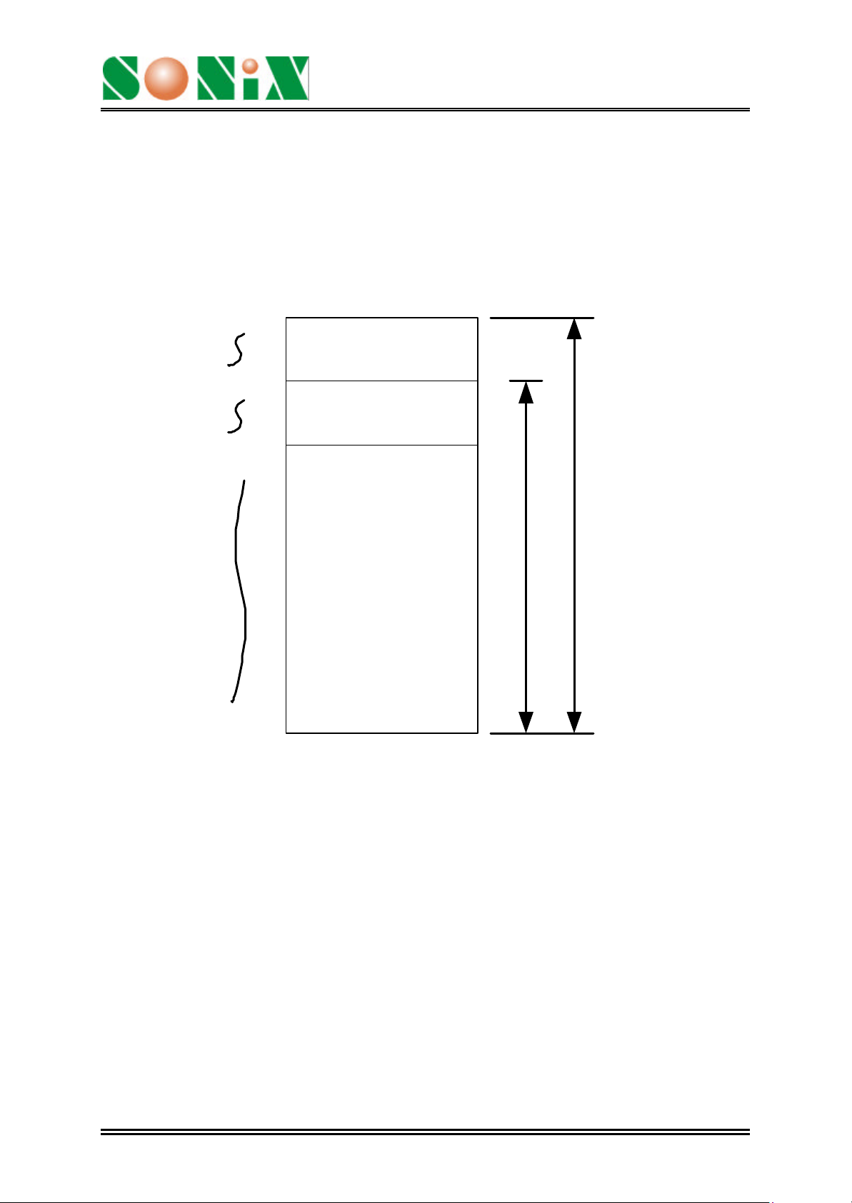
4. ROM TABLE
The total ROM size is 128K words. But only 64K words ROM for programming.
And 32K words of all is the high speed program ROM. The high -low speed ratio is 1:16,
that is to say, if the instruction cycle is two clocks at high speed ROM, the instruction cycle
will down to 32 clocks at low speed ROM.
0x000000
Hi-Speed ROM
(32K words)
0x007FFF
0x008000
0x00FFFF
0x010000
Low-Speed program
ROM
(32K words)
Low-Speed Data ROM (96K words)
Total ROM size (128K words)
0x01FFFF
Data ROM
Ver:1.2 October 23, 2002
SNC725
4
16-bit Voice Processor
5. RAM TABLE
Total RAM size is 2K words, and one bank is 512 words. If user need playing voice
(2Kbps, 3.6Kbps, 12Kbps, dual-tone melody and 4-ch wave -table melody), the system
will reserve 1.5K words RAM size.
0x0000
Bank0
0x01FF
0x0200
Bank1
0x03FF
0x0400
Bank2
0x05FF
0x0600
Bank3 Free for User
0x07FF
Reserved for
OS and Voice
Algorithm
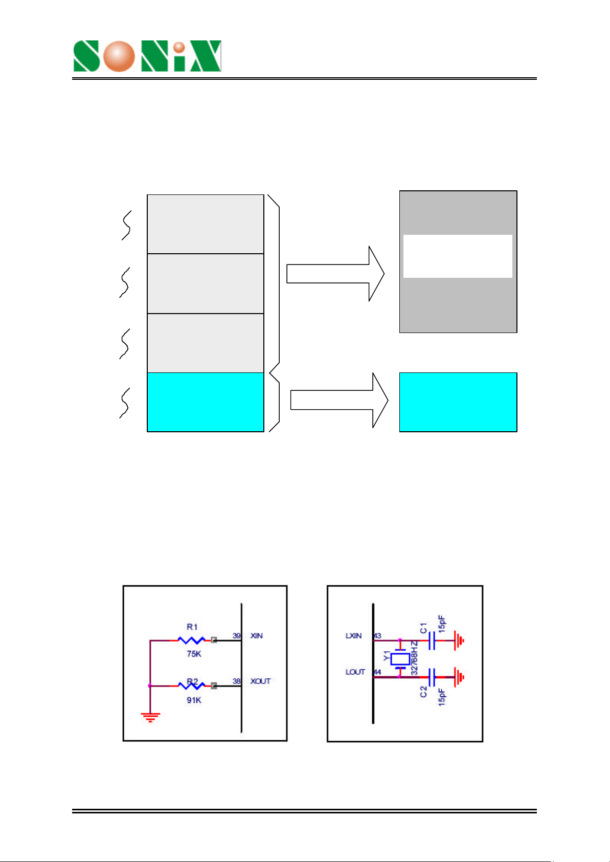
6. System Clock
The system clock source can be selected from 16Mhz crystal or ROSC. For the ROSC,
user should connect two resistors in the pin “XIN” and “XOUT” instead of 16MHZ crystal.
Beside, the clock source select pin “CKSEL” also should be connected to VDD for ROSC.
In order to get an accurate system clock by ROSC, the real time clock source is
recommended to connect a 32768HZ crystal for system clock calibration.
Ver:1.2 October 23, 2002
SNC725
5
Input Control
16-bit Voice Processor
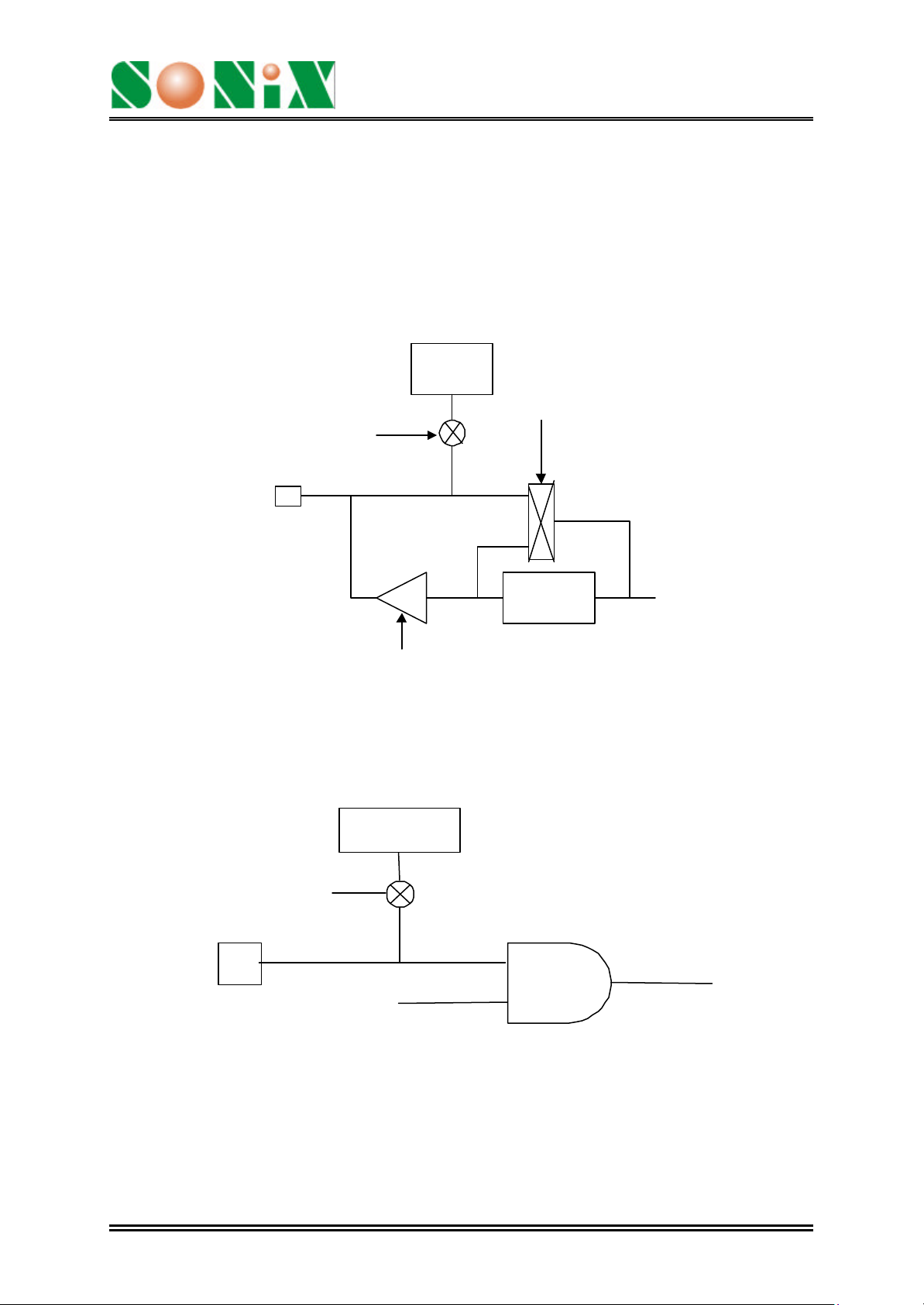
7. I/O PORT
SNC725 provides one a 16-bit I/O port and an 8-bit input port for user application
(P0.0~P0.15, P1.0~P1.7). The input pull high resistor of each pin can be programmed by
Port Pull-High register. The direction of I/O port is selected by Port Direction register. The
Port0 (P0.0~P0.15) and Port1 (P1.0~P1.7) can wake the chip up from the stop mode and
watch mode. P0.15 can be modulated with a 38.5Khz carry signal to realize IR signal
transmission.
Pull-Up
Resister
In/Out
Pull-Up
Select
PAD
Control
Latch
In/Out
Control
to internal bus
I/O Configuration of P0.0~P0.15
Pull-Up
Resister
PAD
Input Port Configuration of Port 1 (P1.0~P1.7)
Ver:1.2 October 23, 2002
 Loading...