

SONIX SN8P1808Q Datasheet
SN8P1800
8-bit micro-controller build-in 12-bit ADC + 72 dots LCD driver
SN8P1800 Series
USER’S MANUAL
General Release Specification
SN8P1808
S
O
Nii
S
O
SONIX reserves the right to make change without further notice to any products herein to improve reliability, function or design. SONIX does not
assume any liability arising out of the application or use of any product or circuit described herein; neither does it convey any license under its patent
rights nor the rights of others. SONIX products are not designed, intended, or authorized for us as components in systems intended, for surgical
implant into the body, or other applications intended to support or sustain life, or for any other application in which the failure of the SONIX product
could create a situation where personal injury or death may occur. Should Buyer purchase or use SONIX products for any such unintended or
unauthorized application. Buyer shall indemnify and hold SONIX and its officers, employees, subsidiaries, affiliates and distributors harmless against
all claims, cost, damages, and expenses, and reasonable attorney fees arising out of, directly or indirectly, any claim of personal injury or death
associated with such unintended or unauthorized use even if such claim alleges that SONIX was negligent regarding the design or manufacture of
the part.
N
X 88--
X
Biitt
B
Miiccrroo--
M
Coonnttrroolllleerr
C
SONiX TECHNOLOGY CO., LTD Revision 1.94
SN8P1800
8-bit micro-controller build-in 12-bit ADC + 72 dots LCD driver
AMENDMENT HISTORY
Version Date Description
VER 1.90 Sep. 2002 V1.90 first issue
VER 1.93 Feb. 2003 1. Extend chip operating temperature from “0°C ~ +70°C” to “-20°C ~ +70°C”.
2. Change the description of ADD M,A instruction from “M M+A” to “M A+M”
3. Add ADC grade.
4. Change bit name and initial value of RBANK register.
5. Change “ACC can’t be access by “B0MOV” instruction” to “ACC can’t be access by
“B0MOV” instruction during the instant addressing mode”.
6. Correct the description of STKnH.
7. Correct the bit definition of INTEN register.
8. Change “The low-speed clock frequency is supplied through on-chip RC oscillator
circuit” to “The low-speed clock frequency is supplied through external low clock
oscillator (32.768K) by crystal or RC mode”.
9. Change all “internal low-speed clock” to “external low-speed clock”.
10. Correct the description of “TC0 CLOCK FREQUENCY OUTPUT” section.
11. Correct the description of “TC1 CLOCK FREQUENCY OUTPUT” section.
12. SCKMD = 1 means SIO is in SLAVE mode. SCKMD = 0 means SIO is in MASTER
mode.
13. Remove “SIO clock and SPI clock are compatible”.
14. Remove this line: “B0MOV A, P2”. P2 of SN8P1808 is output only.
15. Note: The clock source of LCD driver is external low clock.
16. Modify the description ADR register.
17. Modify ADB’s output data table.
18. Correct an error of template code: “b0bclr FWDRST” “b0bset FWDRST”.
19. Add a notice about OSCM register access cycle.
20. Add slow mode (high clock stop and LVD OFF) operating current.
VER 1.94 Sep. 2003 1. Correct RAM Bank value.
2. Correct EOC description.
3. Correct watchdog timer overflow time.
4. Correct POP operand.
5. Correct ADCKS table.
6. Modify figure 11-1 (adjust circuit of LCD contrast) and related description.
7. Add new section about checksum calculate must avoid 04H~07H
8. Correct description of Port6 as I/O port in Chapter 10.
9. Add WTCKS bit in OSCM register
10. Add TC0CKS/TC1CKS in TC0M/TC1M
11. Reserved Last 16 word ROM addresses
SONiX TECHNOLOGY CO., LTD Revision 1.94
SN8P1800
8-bit micro-controller build-in 12-bit ADC + 72 dots LCD driver
12. Add SIOM Table and Note for SIO Rate
13. Remove register bit description
14. Modify TC0M description
15. Modify TC1M description
16. Modify PWM description
17. Modify ADC Frequency description.
18. Change watchdog over flow table.
19. Change Code option table Chapter 2
20. Add ADC current consumption
21. Add LVD detect voltage
22. Modify electrical characteristic table
23. Remove approval sheet.
24. Remove PCB layout notice section.
25. Modify the description of INTRQ register.
26. Modify the calculation formula of SIOR and SIO clock.
SONiX TECHNOLOGY CO., LTD Page 3 Revision 1.94

SN8P1800
8-bit micro-controller build-in 12-bit ADC + 72 dots LCD driver
Table of Contents
AMENDMENT HISTORY.............................................................................................................. 2
1
1
1
PRODUCT OVERVIEW ................................................................................................... 10
GENERAL DESCRIPTION ......................................................................................................... 10
FEATURES SELECTION TABLE ............................................................................................... 10
ADC GRADE TABLE................................................................................................................... 10
FEATURES................................................................................................................................. 11
SYSTEM BLOCK DIAGRAM ...................................................................................................... 12
PIN ASSIGNMENT..................................................................................................................... 13
PIN DESCRIPTIONS.................................................................................................................. 14
PIN CIRCUIT DIAGRAMS .......................................................................................................... 15
2
2
2
3
3
3
CODE OPTION TABLE................................................................................................... 17
ADDRESS SPACES........................................................................................................ 18
PROGRAM MEMORY (ROM)..................................................................................................... 18
OVERVIEW............................................................................................................................. 18
USER RESET VECTOR ADDRESS (0000H).......................................................................... 19
INTERRUPT VECTOR ADDRESS (0008H)............................................................................ 19
CHECKSUM CALCULATION.................................................................................................. 21
GENERAL PURPOSE PROGRAM MEMORY AREA.............................................................. 22
LOOKUP TABLE DESCRIPTION............................................................................................ 22
JUMP TABLE DESCRIPTION................................................................................................. 24
DATA MEMORY (RAM).............................................................................................................. 26
OVERVIEW............................................................................................................................. 26
RAM BANK SELECTION ........................................................................................................ 27
WORKING REGISTERS............................................................................................................. 28
H, L REGISTERS.................................................................................................................... 28
SONiX TECHNOLOGY CO., LTD Page 4 Revision 1.94

SN8P1800
8-bit micro-controller build-in 12-bit ADC + 72 dots LCD driver
Y, Z REGISTERS.................................................................................................................... 29
X REGISTERS........................................................................................................................ 30
R REGISTERS........................................................................................................................ 30
PROGRAM FLAG....................................................................................................................... 31
CARRY FLAG ......................................................................................................................... 31
DECIMAL CARRY FLAG......................................................................................................... 31
ZERO FLAG............................................................................................................................ 31
ACCUMULATOR ........................................................................................................................ 32
STACK OPERATIONS................................................................................................................33
OVERVIEW............................................................................................................................. 33
STACK REGISTERS............................................................................................................... 34
STACK OPERATION EXAMPLE............................................................................................. 35
PROGRAM COUNTER............................................................................................................... 36
ONE ADDRESS SKIPPING .................................................................................................... 37
MULTI-ADDRESS JUMPING.................................................................................................. 38
4
4
4
5
5
5
ADDRESSING MODE...................................................................................................... 39
OVERVIEW................................................................................................................................. 39
IMMEDIATE ADDRESSING MODE........................................................................................ 39
DIRECTLY ADDRESSING MODE .......................................................................................... 39
INDIRECTLY ADDRESSING MODE....................................................................................... 39
TO ACCESS DATA in RAM BANK 0 ....................................................................................... 40
TO ACCESS DATA in RAM BANK 1 ....................................................................................... 40
TO ACCESS DATA in RAM BANK 15 (LCD RAM) ................................................................. 40
SYSTEM REGISTER....................................................................................................... 41
OVERVIEW................................................................................................................................. 41
SYSTEM REGISTER ARRANGEMENT (BANK 0)..................................................................... 41
BYTES of SYSTEM REGISTER.............................................................................................. 41
BITS of SYSTEM REGISTER ................................................................................................. 42
6
6
6
SONiX TECHNOLOGY CO., LTD Page 5 Revision 1.94
POWER ON RESET ........................................................................................................ 44

SN8P1800
8-bit micro-controller build-in 12-bit ADC + 72 dots LCD driver
OVERVIEW................................................................................................................................. 44
EXTERNAL RESET DESCRIPTION........................................................................................... 45
LOW VOLTAGE DETECTOR (LVD) DESCRIPTION.................................................................. 46
7
7
7
OSCILLATORS................................................................................................................ 47
OVERVIEW................................................................................................................................. 47
CLOCK BLOCK DIAGRAM..................................................................................................... 47
OSCM REGISTER DESCRIPTION......................................................................................... 48
OPTION REGISTER DESCRIPTION...................................................................................... 48
EXTERNAL HIGH-SPEED OSCILLATOR............................................................................... 49
OSCILLATOR MODE CODE OPTION.................................................................................... 49
OSCILLATOR DEVIDE BY 2 CODE OPTION......................................................................... 49
OSCILLATOR SAFE GUARD CODE OPTION ....................................................................... 49
SYSTEM OSCILLATOR CIRCUITS........................................................................................ 50
External RC Oscillator Frequency Measurement .................................................................... 51
SYSTEM MODE DESCRIPTION................................................................................................ 52
OVERVIEW............................................................................................................................. 52
NORMAL MODE.....................................................................................................................52
SLOW MODE.......................................................................................................................... 52
GREEN MODE........................................................................................................................ 52
POWER DOWN MODE........................................................................................................... 52
SYSTEM MODE CONTROL....................................................................................................... 53
SN8P1800 SYSTEM MODE BLOCK DIAGRAM..................................................................... 53
SYSTEM MODE SWITCHING ................................................................................................ 54
WAKEUP TIME........................................................................................................................... 55
OVERVIEW............................................................................................................................. 55
HARDWARE WAKEUP........................................................................................................... 55
8
8
8
SONiX TECHNOLOGY CO., LTD Page 6 Revision 1.94
TIMERS COUNTERS....................................................................................................... 56
WATCHDOG TIMER (WDT)....................................................................................................... 56
BASIC TIMER 0 ( T0 ) ................................................................................................................ 57
OVERVIEW............................................................................................................................. 57
T0M REGISTER DESCRIPTION ............................................................................................ 57
T0C COUNTING REGISTER.................................................................................................. 58

SN8P1800
8-bit micro-controller build-in 12-bit ADC + 72 dots LCD driver
T0 BASIC TIMER OPERATION SEQUENCE......................................................................... 59
TIMER COUNTER 0 (TC0)......................................................................................................... 60
OVERVIEW............................................................................................................................. 60
TC0M MODE REGISTER........................................................................................................ 61
TC0C COUNTING REGISTER................................................................................................ 62
TC0R AUTO-LOAD REGISTER.............................................................................................. 63
TC0 TIMER COUNTER OPERATION SEQUENCE................................................................ 64
TC0 CLOCK FREQUENCY OUTPUT (BUZZER).................................................................... 66
TC0OUT FREQUENCY TABLE.................................................................................................. 67
TIMER COUNTER 1 (TC1)......................................................................................................... 69
OVERVIEW............................................................................................................................. 69
TC1M MODE REGISTER........................................................................................................ 70
TC1C COUNTING REGISTER................................................................................................ 71
TC1R AUTO-LOAD REGISTER.............................................................................................. 72
TC1 TIMER COUNTER OPERATION SEQUENCE................................................................ 73
TC1 CLOCK FREQUENCY OUTPUT (BUZZER).................................................................... 75
PWM FUNCTION DESCRIPTION.............................................................................................. 76
OVERVIEW............................................................................................................................. 76
PWM PROGRAM DESCRIPTION........................................................................................... 77
9
9
9
INTERRUPT..................................................................................................................... 78
OVERVIEW................................................................................................................................. 78
INTEN INTERRUPT ENABLE REGISTER ................................................................................. 79
INTRQ INTERRUPT REQUEST REGISTER.............................................................................. 79
INTERRUPT OPERATION DESCRIPTION................................................................................ 80
GIE GLOBAL INTERRUPT OPERATION ............................................................................... 80
INT0 (P0.0) INTERRUPT OPERATION .................................................................................. 81
INT1 (P0.1) INTERRUPT OPERATION .................................................................................. 81
INT2 (P0.2) INTERRUPT OPERATION .................................................................................. 82
T0 INTERRUPT OPERATION................................................................................................. 83
TC0 INTERRUPT OPERATION.............................................................................................. 84
TC1 INTERRUPT OPERATION.............................................................................................. 85
SIO INTERRUPT OPERATION............................................................................................... 86
MULTI-INTERRUPT OPERATION.......................................................................................... 87
SONiX TECHNOLOGY CO., LTD Page 7 Revision 1.94

SN8P1800
8-bit micro-controller build-in 12-bit ADC + 72 dots LCD driver
1
1
1
0
0
0
OVERVIEW................................................................................................................................. 89
SIOM MODE REGISTER............................................................................................................ 90
SIOB DATA BUFFER.................................................................................................................. 91
SIOR REGISTER DESCRIPTION .............................................................................................. 91
SIO MASTER OPERATING DESCRIPTION .............................................................................. 92
RISING EDGE TRANSMITTER/RECEIVER MODE................................................................ 92
FALLING EDGE TRANSMITTER/RECEIVER MODE............................................................. 93
RISING EDGE RECEIVER MODE.......................................................................................... 94
FALLING EDGE RECEIVER MODE ....................................................................................... 95
SIO SLAVE OPERATING DESCRIPTION.................................................................................. 96
RISING EDGE TRANSMITTER/RECEIVER MODE................................................................ 97
FALLING EDGE TRANSMITTER/RECEIVER MODE............................................................. 98
RISING EDGE RECEIVER MODE.......................................................................................... 99
FALLING EDGE RECEIVER MODE ..................................................................................... 100
SIO INTERRUPT OPERATION DESCRIPTION....................................................................... 101
SERIAL INPUT/OUTPUT TRANSCEIVER (SIO).................................................. 89
1
1
1
1
1
1
1
1
1
OVERVIEW............................................................................................................................... 102
I/O PORT FUNCTION TABLE .................................................................................................. 103
PULL-UP RESISTOR (P
I/O PORT MODE ...................................................................................................................... 104
THE P0.3~P0.5 DISCRIPTION................................................................................................. 105
THE PORT2 DISCRIPTION...................................................................................................... 106
THE PORT3 DISCRIPTION...................................................................................................... 107
OPTION Register.................................................................................................................. 107
THE PORT6 DISCRIPTION...................................................................................................... 108
LCDM Register...................................................................................................................... 108
I/O PORT DATA REGISTER .................................................................................................... 110
2
2
2
I/O PORT............................................................................................................. 102
NUR) REGISTER ............................................................................... 103
LCD DRIVER....................................................................................................... 112
SONiX TECHNOLOGY CO., LTD Page 8 Revision 1.94

SN8P1800
8-bit micro-controller build-in 12-bit ADC + 72 dots LCD driver
LCDM REGISTER .................................................................................................................... 112
LCD TIMING............................................................................................................................. 113
LCD RAM LOCATION............................................................................................................... 114
1
1
1
1
1
1
3
3
3
OVERVIEW............................................................................................................................... 115
ADM REGISTER....................................................................................................................... 116
ADR REGISTERS..................................................................................................................... 116
ADB REGISTERS..................................................................................................................... 116
ADC CONVERTING TIME........................................................................................................ 118
ADC CIRCUIT........................................................................................................................... 119
4
4
4
TEMPLATE CODE.................................................................................................................... 120
CHIP DECLARATION IN ASSEMBLER.................................................................................... 124
PROGRAM CHECK LIST ......................................................................................................... 124
8-CHANNEL ANALOG TO DIGITAL CONVERTER........................................... 115
CODING ISSUE .................................................................................................. 120
1
1
1
1
1
1
1
1
1
SONiX TECHNOLOGY CO., LTD Page 9 Revision 1.94
5
5
5
6
6
6
ABSOLUTE MAXIMUM RATING.............................................................................................. 126
STANDARD ELECTRICAL CHARACTERISTIC....................................................................... 126
7
7
7
INSTRUCTION SET TABLE ............................................................................... 125
ELECTRICAL CHARACTERISTIC ..................................................................... 126
PACKAGE INFORMATION ................................................................................ 127
SN8P1800
8-bit micro-controller build-in 12-bit ADC + 72 dots LCD driver
1
1
1
PRODUCT OVERVIEW
GENERAL DESCRIPTION
The SN8P1800 is an series of 8-bit micro-controller including SN8P1808. This series is utilized with CMOS technology
fabrication and featured with low power consumption and high performance by its unique electronic structure.
These chips are designed with the excellent IC structure including the large program memory OTP ROM, the massive
data memory RAM, one 8-bit basic timer (T0), two 8-bit timer counters (TC0, TC1), high performance of real time clock
timer (RTC) , a watchdog timer, up to seven interrupt sources (T0, TC0, TC1, SIO, INT0, INT1, INT2), an 8-channel
ADC converter with 8-bit/12-bit resolution, two channel PWM output (PWM0, PWM1), tw0 channel buzzer output (BZ0,
BZ1) and 8-level stack buffers.
Besides, the user can choose desired oscillator configurations for the controller. There are four oscillator configurations
to select for generating system clock, including High/Low speed crystal, ceramic resonator or cost-saving RC.
SN8P1800 series is a dual clock system using a hi-speed crystal for normal mode operation and an external low speed
crystal for slow mode, real time clock and LCD function.
FEATURES SELECTION TABLE
CHIP ROM RAM Stack
SN8P1808 4K*16 256 8 V V V 47 8ch 2 1 10 LQPF64
Timer PWM Wakeup
T0 TC0 TC1
Table 1-1. Selection Table of SN8P1800
I/O ADC DAC
SIO
Buzzer
Pin no.
Package
ADC GRADE TABLE
CHIP PARAMETER MIN MAX UNITS REMARK
Resolution 12 Bits
SN8P1808
SN8P1808-12
No Mission Code 8 12 Bits
Differential Nonlinearity (DNL) 16 LSB
Resolution 12 Bits
No Mission Code 10 12 Bits
Differential Nonlinearity (DNL) 4 LSB
Table 1-2. ADC Grade Table
SONiX TECHNOLOGY CO., LTD Page 10 Revision 1.94

SN8P1800
8-bit micro-controller build-in 12-bit ADC + 72 dots LCD driver
FEATURES
SN8P1808
Memory configuration
OTP ROM size: 4K * 16 bits
RAM size: 256 * 8 bits (bank 0 and bank 1)
LCD RAM size: 24 * 3 bits
I/O pin configuration
Input only: P0, P3
Output only: P2 shared with LCD segment
Bi-directional: P1, P4, P5, P6
Wakeup: P0, P1
Pull-up resisters: P0, P1, P3, P4, P5, P6
External interrupt: P0
Port 3 shared with LCD segment
All LCD pins shared with the I/O pins
59 powerful instructions
Four clocks per instruction cycle
All of instructions are one word length.
Most of instructions are one cycle only.
Maximum instruction cycle is two.
All ROM area JMP instruction.
All ROM area lookup table function (MOVC)
Support hardware multiplier (MUL).
Seven interrupt sources
Four internal interrupts: T0, TC0, TC1, SIO
Three external interrupts: INT0, INT1, INT2
A real time clock timer
An 8-bit basic timer with green mode wakeup
function
Two 8-bit timer counters with PWM or buzzer
On chip watchdog timer
Eight levels stack buffer
An 8-channel ADC with 8-bit/12-bit resolution
SIO function
LCD driver: 1/3 duty, 1/2 bias. 3 common * 24
segment
Dual clock system offers four operating modes
External high clock: RC type up to 10 MHz
External high clock: Crystal type up to 16 MHz
External Low clock: Crystal 32768Hz
Normal mode: Both high and low clock active.
Slow mode: Low clock only.
Sleep mode: Both high and low clock stop.
Green mode: Periodical wakeup by timer.
Package
Chip form: LQFP 64 pins
SONiX TECHNOLOGY CO., LTD Page 11 Revision 1.94
SN8P1800
8-bit micro-controller build-in 12-bit ADC + 72 dots LCD driver
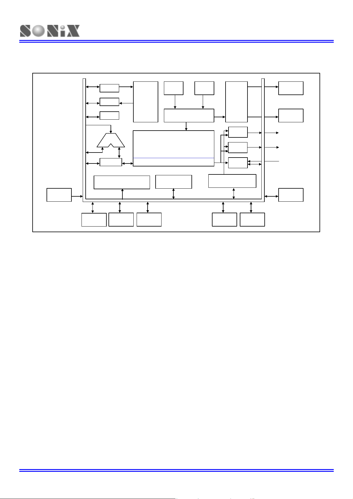
SYSTEM BLOCK DIAGRAM
H-OSC
PC
PC
OTP
OTP
ROM
IR
IR
FLAGS
FLAGS
ALU
ALU
ACC
ACC
INTERRUPT CONTROL
INTERRUPT CONTROLINTERRUPT CONTROL
ROM
H-OSC
TIMING GENERATOR
TIMING GENERATOR
RAM
RAM
SYSTEM REGISTE R
SYSTEM REGISTE R
SIO TX/RX
SIO TX/RXSIO TX/RX
L-OSC
L-OSC
TIMER & COUNTER
TIMER & COUNTER
LCD
LCD
DRIVER
DRIVER
PWM1
PWM1PWM1
PWM0
PWM0PWM0
ADC
ADC
COM.
COM.
SEG.
SEG.
PWM1/Buzzer1
PWM1/Buzzer1
PWM0/Buzzer0
PWM0/Buzzer0
AIN0~AIN7
AIN0~AIN7
PORT 0
PORT 0
PORT 1
PORT 1
PORT 2 PORT 3 PORT 4 PORT 5
PORT 2 PORT 3 PORT 4 PORT 5
Figure 1-1.Simplified System Block Diagram
PORT 6
PORT 6
SONiX TECHNOLOGY CO., LTD Page 12 Revision 1.94
SN8P1800
8-bit micro-controller build-in 12-bit ADC + 72 dots LCD driver
PIN ASSIGNMENT
SN8P1808 (LQFP64)
P0.0/INT0 2 O 47SEG15/P3.7
P0.1/INT1 3 46SEG16/P2.0
P0.2/INT24 45SEG17/P2.1
P1.05 44SEG18/P2.2
P1.16 43SEG19/P2.3
P1.27 42SEG20/P2.4
P1.3 8 SN8P1808Q 41 SEG21/P2.5
VDD9 40SEG22/P2.6
AVREFH 10 39 SEG23/P2.7
P4.0/AIN011 38COM0/P0.3
P4.1/AIN112 37COM1/P0.4
P4.2/AIN213 36COM2/P0.5
P4.3/AIN314 35V1
P4.4/AIN415 34V2
P4.5/AIN516 33VLCD
VSS
SEG0/P6.0
SEG1/P6.1
SEG2/P6.2
SEG3/P6.3
SEG4/P6.4
SEG5/P6.5
SEG6/P6.6
SEG7/P6.7
SEG8/P3.0
VDD
SEG9/P3.1
SEG10/P3.2
SEG11/P3.3
SEG12/P3.4
SEG13/P3.5
64 63 62 61 60 59 58 57 56 55 54 53 52 51 50 49
RST1 48SEG14/P3.6
17 18 19 20 21 22 23 24 25 26 27 28 29 30 31 32
LXIN
LXOUT
XIN
XOUT
AVREFL
P4.6/AIN6
P4.7/AIN7
VSS
AVSS
P5.1/SI
P5.2/SO
P5.0/SCK
P5.3/BZ1/PWM1
P5.4/BZ0/PWM0
VDD
VPP/VDD
SONiX TECHNOLOGY CO., LTD Page 13 Revision 1.94
SN8P1800
8-bit micro-controller build-in 12-bit ADC + 72 dots LCD driver
PIN DESCRIPTIONS
PIN NAME TYPE DESCRIPTION
VDD, VSS P Power supply input pins for digital circuit.
AVDD, AVSS P Power supply input pins for analog circuit.
VPP P OTP ROM programming pin. Connect to VDD in normal operation.
RST I System reset input pin. Schmitt trigger structure, active “low”, normal stay to “high”.
XIN, XOUT I, O External oscillator pins. RC mode from XIN.
LXIN, LXOUT I, O Low speed (32768 Hz) oscillator pins. RC mode from LXIN.
P0.0 / INT0 I Port 0.0 and shared with INT0 trigger pin. (Schmitt trigger) / Built-in pull-up resisters.
P0.1 / INT1 I Port 0.1 and shared with INT1 trigger pin. (Schmitt trigger) / Built-in pull-up resisters.
P0.2 / INT2 I Port 0.2 and shared with INT2 trigger pin. (Schmitt trigger) / Built-in pull-up resisters.
P0.3~ P0.5 I
P1.0 ~ P1.3 I/O Port 1.0~Port 1.3 bi-direction pins / Built-in pull-up resisters.
P2.0 ~ P2.7 O Port 2.0~Port 2.7 output only port and shared with LCD’s SEG16~SEG23.
P3.0 ~ P3.7 I
P4.0 ~ P4.7 I/O Port 4.0~Port 4.7 bi-direction pins / Built-in pull-up resisters.
P5.0 / SCK I/O Port 5.0 bi-direction pin and SIO’s clock input/output / Built-in pull-up resisters.
P5.1 / SI I/O Port 5.1 bi-direction pin and SIO’s data input / Built-in pull-up resisters.
P5.2 / SO I/O Port 5.2 bi-direction pin and SIO’s data output / Built-in pull-up resisters.
P5.3 / BZ1 / PWM1 I/O
P5.4 / BZ0 / PWM0 I/O
P6.0 ~ P6.7 I/O
AIN0 ~ AIN7 I Analog signal input pins for ADC converter.
COM0 ~ COM2 O LCD driver common pins.
SEG0 ~ SEG23 O LCD driver segment pins.
AvrefH,AverfL I ADC’s reference high / low voltage input pins.
Port 0.3~Port 0.5 input pins and shared with LCD’s COM0~COM2. (Schmitt trigger).
Built-in pull-up resisters.
Port 3.0~Port 3.7 input port with pull-up resister and shared with LCD’s SEG8~SEG15.
Built-in pull-up resisters.
Port 5.3 bi-direction pin, TC1 ÷ 2 signal output pin or PWM1 output pin.
Built-in pull-up resisters.
Port 5.4 bi-direction pin, TC0 ÷ 2 signal output pin or PWM0 output pin.
Built-in pull-up resisters.
Port 6.0 ~ Port 6.7 bi-direction pins and shared with LCD’s SEG0~SEG7.
Enable pull-up resisters in input mode automatically.
Table 1-3. SN8P1800 Pin Description
SONiX TECHNOLOGY CO., LTD Page 14 Revision 1.94
SN8P1800
8-bit micro-controller build-in 12-bit ADC + 72 dots LCD driver
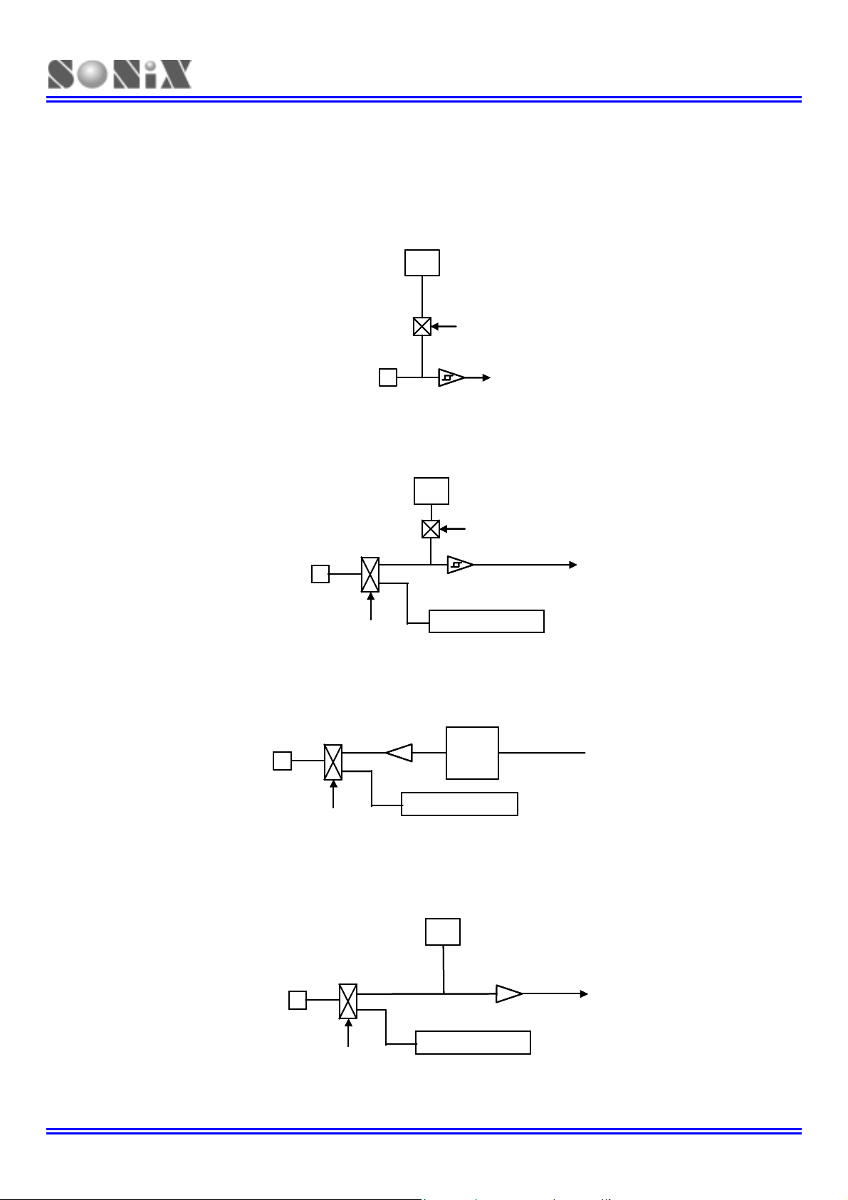
PIN CIRCUIT DIAGRAMS
Port0.0~P0.2 structure
Port0.0~P0.2 structure
PUR
PUR
P0UR
P0UR
Pin
Pin
Port0.3~P0.5 structure
Port0.3~P0.5 structure
Port0.3~P0.5 structure
Port0.3~P0.5 structure
Int. bus
Int. bus
PUR
PUR
PUR
PUR
P0UR
P0URP0UR
Int. bus
Int. bus
Pin
PinPin
LCD waveform
LCD Code Option
LCD Code Option
LCD waveformLCD waveform
Port2 structure
Port2 structure
Int. bus
Int. bus
Pin
PinPin
LCD Code Option
LCD Code Option
Latch
Latch
LCD waveform
LCD waveform
LCD waveform
Port3 structure
Port3 structure
Port3 structure
PUR
PUR
PUR
Int. bus
Int. bus
Pin
PinPin
LCD waveform
LCD waveformLCD waveform
P3LCD
P3LCD
SONiX TECHNOLOGY CO., LTD Page 15 Revision 1.94
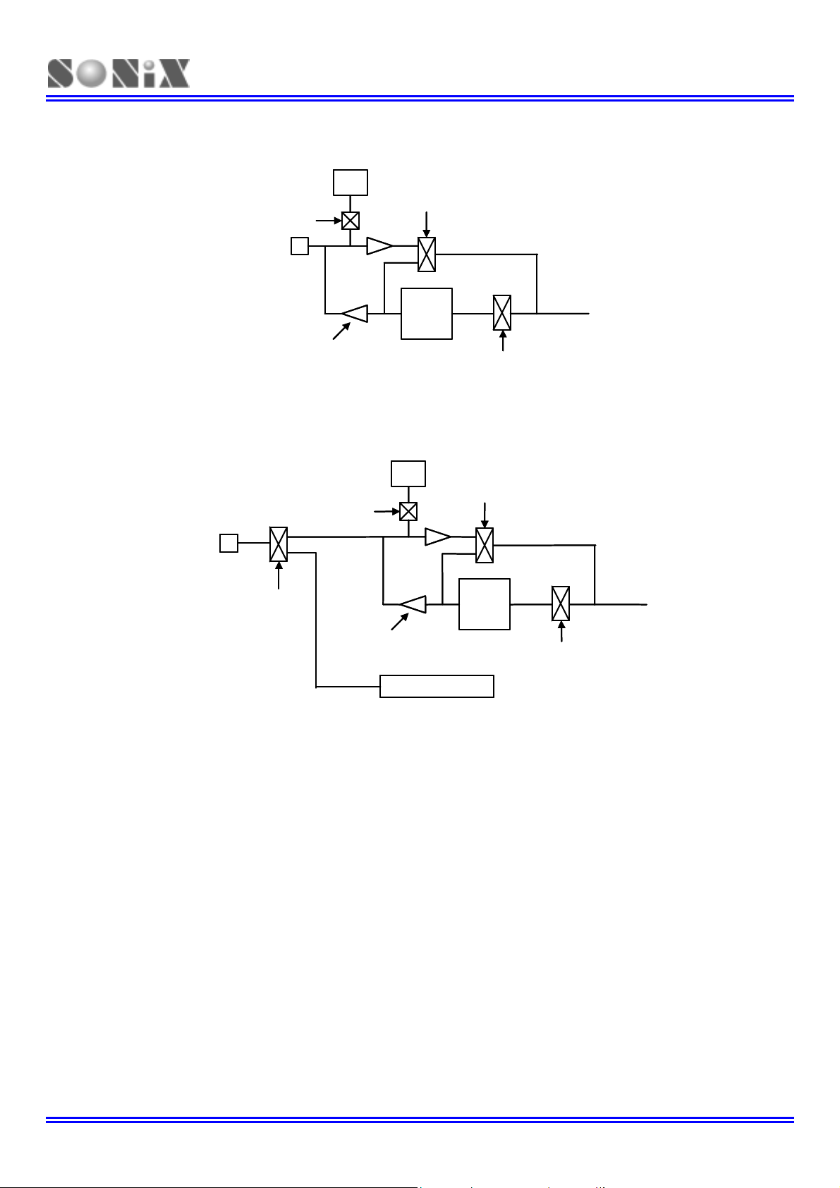
SN8P1800
8-bit micro-controller build-in 12-bit ADC + 72 dots LCD driver
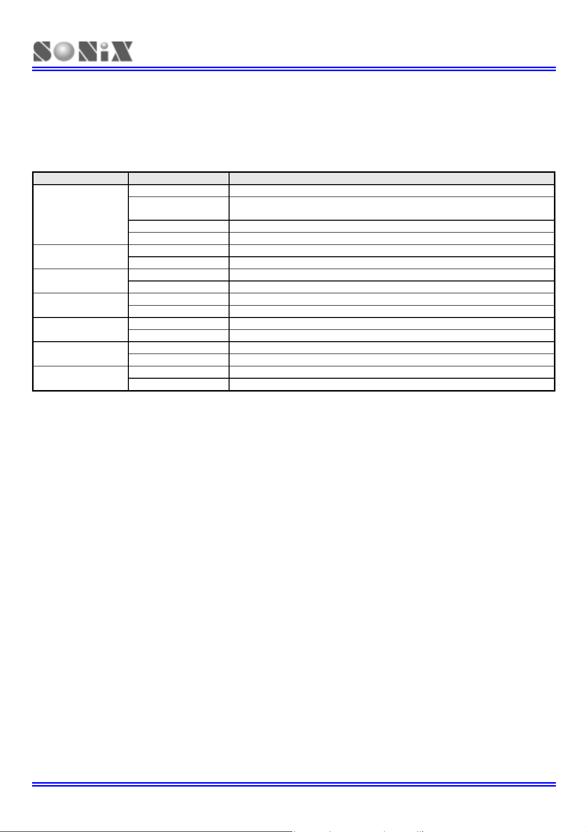
Port1,Port4,Port5 structure
Port1,Port4,Port5 structure
PUR
PUR
PnM
PnM
PnM, PnUR
PnM, PnUR
Pin
Pin
Int. bus
Latch
Latch
PnM
PnM
PnM
PnM
Port6 structure
Port6 structure
PUR
PUR
PnM
PnM
PnM
PnM
Int. bus
Pin
PinPin
Int. bus
P6HSEG, P6LSEG
P6HSEG, P6LSEG
PnM
PnM
LCD waveform
LCD waveformLCD wavef orm
Latch
Latch
PnM
PnM
Int. bus
Figure 1-2. Pin Circuit Diagram
SONiX TECHNOLOGY CO., LTD Page 16 Revision 1.94
SN8P1800
8-bit micro-controller build-in 12-bit ADC + 72 dots LCD driver
2
2
2
Code Option Content Function Description
High_Clk
High_Clk / 2
OSG
Watch_Dog
LVD
Security
LCD
CODE OPTION TABLE
RC Low cost RC for external high clock oscillator
32K X’tal
12M X’tal High speed crystal /resonator (e.g. 12M) for external high clock oscillator
4M X’tal Standard crystal /resonator (e.g. 3.58M) for external high clock oscillator
Enable External high clock divided by two, Fosc = high clock / 2
Disable Fosc = high clock
Enable Enable Oscillator Safe Guard function
Disable Disable Oscillator Safe Guard function
Enable Enable Watch Dog function
Disable Disable Watch Dog function
Enable Enable the low voltage detect
Disable Disable the low voltage detect
Enable Enable ROM code Security function
Disable Disable ROM code Security function
Enable Enable LCD function
Disable Disable LCD function
Low frequency, power saving crystal (e.g. 32.768K) for external high
clock oscillator
Table 2-1. Code Option Table of SN8P1800
SONiX TECHNOLOGY CO., LTD Page 17 Revision 1.94
SN8P1800
8-bit micro-controller build-in 12-bit ADC + 72 dots LCD driver
3
3
3
ADDRESS SPACES
PROGRAM MEMORY (ROM)
OVERVIEW
ROM Maps for SN8P1800 devices provide 4K x 16 OTP memory that programmable by user. The SN8P1800 program
memory is able to fetch instructions through 12-bit wide PC (Program Counter) and can look up ROM data by using
ROM code registers (R, X, Y, Z). In standard configuration, the device’s 4,096 x 16-bit program memory has four
areas:
1-word reset vector addresses
1-word Interrupt vector addresses
5-words reserved area
4K words general purpose area
All of the program memory is partitioned into two coding areas, located from 0000H to 0008H and from 0009H to
0FFEH. The former area is assigned for executing reset vector and interrupt vector. The later area is for storing
instruction’s OP-code and lookup table’s data. User’s program is in the last area (0010H~0FFEH).
0000H
0001H Jump to user start address
0002H Jump to user start address
0003H
0004H
0005H
0006H
0007H
0008H
0009H User program
.
.
000FH
0010H
0011H
.
.
0FFEH
0FFFH
General purpose area
General purpose area
ROM
Reset vector
Reserved
Interrupt vector
Reserved
User reset vector
Jump to user start address
User interrupt vector
End of user program
Figure 3-1. ROM Address Structure
SONiX TECHNOLOGY CO., LTD Page 18 Revision 1.94

SN8P1800
8-bit micro-controller build-in 12-bit ADC + 72 dots LCD driver
USER RESET VECTOR ADDRESS (0000H)
A 1-word vector address area is used to execute system reset. After power on reset or watchdog timer overflow reset,
then the chip will restart the program from address 0000h and all system registers will be set as default values. The
following example shows the way to define the reset vector in the program memory.
Example: After power on reset, external reset active or reset by watchdog timer overflow.
CHIP SN8P1808
ORG 0 ; 0000H
JMP START ; Jump to user program address.
. ; 0001H ~ 0007H are reserved
ORG 10H
START: ; 0010H, The head of user program.
. ; User program
.
.
.
ENDP
; End of program
INTERRUPT VECTOR ADDRESS (0008H)
A 1-word vector address area is used to execute interrupt request. If any interrupt service is executed, the program
counter (PC) value is stored in stack buffer and points to 0008h of program memory to execute the vectored interrupt.
Users have to define the interrupt vector. The following example shows the way to define the interrupt vector in the
program memory.
Example 1: This demo program includes interrupt service routine and the user program is behind the
interrupt service routine.
CHIP SN8P1808
ORG 0 ; 0000H
JMP START ; Jump to user program address.
. ; 0001H ~ 0007H are reserved
ORG 8
START: ; The head of user program.
B0XCH A, ACCBUF
PUSH
.
.
.
POP
B0XCH A, ACCBUF
RETI
.
.
.
.
JMP START
ENDP
; Interrupt service routine
; B0XCH doesn’t change C, Z flag
; Push 80H ~ 87H system registers
; Pop 80H ~ 87H system registers
; End of interrupt service routine
; User program
; End of user program
; End of program
SONiX TECHNOLOGY CO., LTD Page 19 Revision 1.94

SN8P1800
8-bit micro-controller build-in 12-bit ADC + 72 dots LCD driver
Example 2: The demo program includes interrupt service routine and the address of interrupt service
routine is in a special address of general-purpose area.
CHIP SN8P1808
ORG 0 ; 0000H
JMP START ; Jump to user program address.
. ; 0001H ~ 0007H are reserved
ORG 08
JMP MY_IRQ ; 0008H, Jump to interrupt service routine address
ORG 10H
START: ; 0010H, The head of user program.
. ; User program
.
.
.
MY_IRQ: ;The head of interrupt service routine
Remark: It is easy to get the rules of SONIX program from demo programs given above. These points are
as following.
1. The address 0000H is a “JMP” instruction to make the program go to general-purpose ROM area. The
0004H~0007H are reserved. Users have to skip 0004H~0007H addresses. It is very important and
necessary.
2. The interrupt service starts from 0008H. Users can put the whole interrupt service routine from 0008H
(Example1) or to put a “JMP” instruction in 0008H then place the interrupt service routine in other
general-purpose ROM area (Example2) to get more modularized coding style.
JMP START
B0XCH A, ACCBUF
PUSH
.
.
.
POP
B0XCH A, ACCBUF
RETI
ENDP
; End of user program
; B0XCH doesn’t change C, Z flag
; Push 80H ~ 87H system registers
; Pop 80H ~ 87H system registers
; End of interrupt service routine
; End of program
SONiX TECHNOLOGY CO., LTD Page 20 Revision 1.94

SN8P1800
8-bit micro-controller build-in 12-bit ADC + 72 dots LCD driver
CHECKSUM CALCULATION
The ROM addresses 0004H~0007H and last address are reserved area. User should avoid these addresses
(0004H~0007H and last address) when calculate the Checksum value.
Example:
The demo program shows how to avoid 0004H~0007H when calculated Checksum from 00H to the end of
user’s code
MOV A,#END_USER_CODE$L
B0MOV END_ADDR1,A ;save low end address to end_addr1
MOV A,#END_USER_CODE$M
B0MOV END_ADDR2,A ;save middle end address to end_addr2
CLR Y ;set Y to ooH
CLR Z ;set Z to 00H
@@:
CALL YZ_CHECK ;call function of check yz value
MOVC ;
B0BSET FC ;clear C glag
ADD DATA1,A ;add A to Data1
MOV A,R
ADC DATA2,A ;add R to Data2
JMP END_CHECK ;check if the YZ address = the end of code
AAA:
INCMS Z ;Z=Z+1
JMP @B ;if Z!= 00H calculate to next address
JMP Y_ADD_1 ;if Z=00H increase Y
END_CHECK:
MOV A,END_ADDR1
CMPRS A,Z ;check if Z = low end address
JMP AAA ;if Not jump to checksum calculate
MOV A,END_ADDR2
CMPRS A,Y ;if Yes, check if Y = middle end address
JMP AAA ;if Not jump to checksum calculate
JMP CHECKSUM_END ;if Yes checksum calculated is done.
YZ_CHECK: ;check if YZ=0004H
MOV A,#04H
CMPRS A,Z ;check if Z=04H
RET ;if Not return to checksum calculate
MOV A,#00H
CMPRS A,Y ;if Yes, check if Y=00H
RET ;if Not return to checksum calculate
INCMS Z ;if Yes, increase 4 to Z
INCMS Z
INCMS Z
INCMS Z
RET ;set YZ=0008H then return
Y_ADD_1:
INCMS Y ;increase Y
NOP
JMP @B ;jump to checksum calculate
CHECKSUM_END:
……….
……….
END_USER_CODE: ;Label of program end
SONiX TECHNOLOGY CO., LTD Page 21 Revision 1.94

SN8P1800
8-bit micro-controller build-in 12-bit ADC + 72 dots LCD driver
GENERAL PURPOSE PROGRAM MEMORY AREA
The 4089-word at ROM locations 0010H~0FFEH are used as general-purpose memory. The area is stored
instruction’s op-code and look-up table data. The SN8P1800 includes jump table function by using program counter
(PC) and look-up table function by using ROM code registers (R, X, Y, Z).
The boundary of program memory is separated by the high-byte program counter (PCH) every 100H. In jump table
function and look-up table function, the program counter can’t leap over the boundary by program counter
automatically. Users need to modify the PCH value to “PCH+1” as the PCL overflow (from 0FFH to 000H).
LOOKUP TABLE DESCRIPTION
In the ROM’s data lookup function, the X register is pointed to the highest 8-bit, Y register to the middle 8-bit and Z
register to the lowest 8-bit data of ROM address. After MOVC instruction is executed, the low-byte data of ROM then
will be stored in ACC and high-byte data stored in R register.
Example: To look up the ROM data located “TABLE1”.
B0MOV Y, #TABLE1$M ; To set lookup table1’s middle address
B0MOV Z, #TABLE1$L ; To set lookup table1’s low address.
MOVC ; To lookup data, R = 00H, ACC = 35H
;
;
@@:
. . ;
TABLE1: DW 0035H ; To define a word (16 bits) data.
DW 5105H ; “
DW 2012H ; “
CAUSION: The Y register can't increase automatically if Z register cross boundary from 0xFF to 0x00.
Therefore, user must take care such situation to avoid loop-up table errors. If Z register overflow, Y
register must be added one. The following INC_YZ macro shows a simple method to process Y and Z
registers automatically.
Note: Because the program counter (PC) is only 12-bit, the X register is useless in the application. Users
can omit “B0MOV X, #TABLE1$H”. SONiX ICE support more larger program memory addressing
capability. So make sure X register is “0” to avoid unpredicted error in loop-up table operation.
INCMS Z ; Z+1
JMP @F ; Not overflow
INCMS Y ; Z overflow (FFH 00), Y=Y+1
NOP ; Not overflow
MOVC ; To lookup data, R = 51H, ACC = 05H.
; Increment the index address for next address
Example: INC_YZ Macro
INC_YZ MACRO
INCMS Z ; Z+1
JMP @F ; Not overflow
INCMS Y ; Y+1
NOP ; Not overflow
@@:
ENDM
SONiX TECHNOLOGY CO., LTD Page 22 Revision 1.94

SN8P1800
8-bit micro-controller build-in 12-bit ADC + 72 dots LCD driver
The other coding style of loop-up table is to add Y or Z index register by accumulator. Be careful if carry happen. Refer
following example for detailed information:
Example: Increase Y and Z register by B0ADD/ADD instruction
B0MOV Y, #TABLE1$M ; To set lookup table’s middle address.
B0MOV Z, #TABLE1$L ; To set lookup table’s low address.
GETDATA: ;
MOVC ; To lookup data. If BUF = 0, data is 0x0035
; If BUF = 1, data is 0x5105
; If BUF = 2, data is 0x2012
.
.
. . ;
TABLE1: DW 0035H ; To define a word (16 bits) data.
DW 5105H ; “
DW 2012H ; “
B0MOV A, BUF ; Z = Z + BUF.
B0ADD Z, A
B0BTS1 FC ; Check the carry flag.
JMP GETDATA ; FC = 0
INCMS Y ; FC = 1. Y+1.
NOP
SONiX TECHNOLOGY CO., LTD Page 23 Revision 1.94

SN8P1800
8-bit micro-controller build-in 12-bit ADC + 72 dots LCD driver
JUMP TABLE DESCRIPTION
The jump table operation is one of multi-address jumping function. Add low-byte program counter (PCL) and ACC
value to get one new PCL. The new program counter (PC) points to a series jump instructions as a listing table. The
way is easy to make a multi-stage program.
When carry flag occurs after executing of “ADD PCL, A”, it will not affect PCH register. Users have to check if the jump
table leaps over the ROM page boundary or the listing file gener ated by SONIX assembly software. If the jump table
leaps over the ROM page boundary (e.g. from xxFFH to xx00H), move the jump table to the top of next program
memory page (xx00H). Here one page mean 256 words.
Example : If PC = 0323H (PCH = 03H、PCL = 23H)
ORG 0X0100 ; The jump table is from the head of the ROM boundary
B0ADD PCL, A ; PCL = PCL + ACC, the PCH can’t be changed.
JMP A0POINT ; ACC = 0, jump to A0POINT
JMP A1POINT ; ACC = 1, jump to A1POINT
JMP A2POINT ; ACC = 2, jump to A2POINT
JMP A3POINT ; ACC = 3, jump to A3POINT
In following example, the jump table starts at 0x00FD. When execute B0ADD PCL, A. If ACC = 0 or 1, the jump
table points to the right address. If the ACC is larger then 1 will cause error because PCH doesn't increase one
automatically. We can see the PCL = 0 when ACC = 2 but the PCH still keep in 0. The program counter (PC) will
point to a wrong address 0x0000 and crash system operation. It is important to check whether the jump table
crosses over the boundary (xxFFH to xx00H). A good coding style is to put the jump table at the start of ROM
boundary (e.g. 0100H).
Example: If “jump table” crosses over ROM boundary will cause errors.
ROM Address
. .
. .
. .
0X00FD
0X00FE
0X00FF
0X0100
0X0101
. .
. .
SONIX provides a macro for safe jump table function. This macro will check the ROM boundary and move the jump
table to the right position automatically. The side effect of this macro is maybe wasting some ROM size. Notice the
maximum jmp table number for this macro is limited under 254.
@JMP_A MACRO VAL
IF (($+1) !& 0XFF00) !!= (($+(VAL)) !& 0XFF00)
JMP ($ | 0XFF)
ORG ($ | 0XFF)
ENDIF
ADD PCL, A
ENDM
Note: “VAL” is the number of the jump table listing number.
B0ADD PCL, A ; PCL = PCL + ACC, the PCH can’t be changed.
JMP A0POINT ; ACC = 0
JMP A1POINT ; ACC = 1
JMP A2POINT
JMP A3POINT ; ACC = 3
; ACC = 2 jump table cross boundary here
SONiX TECHNOLOGY CO., LTD Page 24 Revision 1.94

SN8P1800
8-bit micro-controller build-in 12-bit ADC + 72 dots LCD driver
Example: “@JMP_A” application in SONIX macro file called “MACRO3.H”.
B0MOV A, BUF0 ; “BUF0” is from 0 to 4.
@JMP_A 5 ; The number of the jump table listing is five.
JMP A0POINT ; If ACC = 0, jump to A0POINT
JMP A1POINT ; ACC = 1, jump to A1POINT
JMP A2POINT ; ACC = 2, jump to A2POINT
JMP A3POINT ; ACC = 3, jump to A3POINT
JMP A4POINT ; ACC = 4, jump to A4POINT
If the jump table position is from 00FDH to 0101H, the “@JMP_A” macro will make the jump table to start from 0100h.
SONiX TECHNOLOGY CO., LTD Page 25 Revision 1.94
SN8P1800
8-bit micro-controller build-in 12-bit ADC + 72 dots LCD driver
DATA MEMORY (RAM)
OVERVIEW
The SN8P1808 has internally built-in the huge data memory up to 256 bytes for storing general purpose data and
featured with LCD memory space up to 24 locations (24 * 3 bits) for displaying pattern.
256 * 8-bit general purpose area
128 * 8-bit system register area
24 * 3-bit LCD memory space
These memory are separated into bank 0, bank1 and bank 15. The user can program RBANK register of RAM bank
selection bit to access all data in any of the three RAM banks. The bank 0 and bank1, using the first 128-byte location
assigned as general-purpose area, and the remaining 128-byte in bank 0 as system register. The bank 15 is LCD RAM
area designed for storing LCD display data.
RAM location
000h General purpose area ; 000h~07Fh of Bank 0 = To store general
. ; purpose data (128 bytes).
BANK 0
BANK 1
200h “ ; reserved
“ ; “
280h “ ; “
“ ; “
300h “ ; “
“ ; “
380h “ ; “
“ ; “
BANK 15
07Fh .
080h System register ; 080h~0FFh of Bank 0 = To store system
. ; registers (128 bytes).
0FFh End of bank 0 area
100h General purpose area ; Bank 1 = To store general purpose data.
.
17Fh End of bank 1 area ; Bank 1 only has 128 bytes RAMs.
F00h LCD RAM area ; Bank 15 = To store LCD display data
. ; (24 bytes).
F17h End of LCD Ram ;
Figure 3-2 RAM Location of SN8P1808
Note:1. The undefined locations of system register area are logic “high” after executing read instruction
“MOV A, M”.
Note:2. The lower 24 locations of bank15 are used to store LCD display data and the other locations are
reserved. The RAMs of LCD data area only have lowest 3-bit to be used. The highest 5-bit are
undefined.
SONiX TECHNOLOGY CO., LTD Page 26 Revision 1.94
SN8P1800
8-bit micro-controller build-in 12-bit ADC + 72 dots LCD driver
RAM BANK SELECTION
The RBANK is a 1-bit register located at 87H in RAM bank 0. The user can access RAM data by using this register
pointing to working RAM bank for ACC to read/write RAM data.
RBANK initial value = xxxx 0000
087H Bit 7 Bit 6 Bit 5 Bit 4 Bit 3 Bit 2 Bit 1 Bit 0
RBANK
- - - - R/W R/W R/W R/W
RBNKn: RAM bank selecting control bit. 0 = bank 0, 1 = bank 1.
Example: RAM bank selecting.
; BANK 0
CLR RBANK
.
; BANK 1
MOV A, #1
B0MOV RBANK, A
.
Note: “B0MOV” instruction can access the RAM of bank 0 in other bank situation directly.
Example: Access RAM bank 0 in RAM bank 1.
; BANK 1
B0BSET RBNKS0 ; Get into RAM bank 1
B0MOV A, BUF0 ; Read BUF0 data. BUF0 is in RAM bank0.
MOV BUF1, A ; Write BUF0 data to BUF1. BUF1 is in RAM bank1.
.
. .
MOV A, BUF1 ; Read BUF1 data and store in ACC.
B0MOV BUF0, A ; Write ACC data to BUF0.
Under bank 1 situation, using “B0MOV” instruction is an easy way to access RAM bank 0 data. User can make a habit
to read/write system register (0087H~00FFH). Then user can access system registers without switching RAM bank.
Example: To Access the system registers in bank 1 situation.
; BANK 1
B0BSET RBNKS0 ; Get into RAM bank 1
. .
MOV A, #0FFH ; Set all pins of P1 to be logic high.
B0MOV P1, A
.
B0MOV A, P0 ; Read P0 data and store into BUF1 of RAM bank 1.
MOV BUF1, A
- - - - RBNKS3 RBNKS2 RBNKS1 RBNKS0
SONiX TECHNOLOGY CO., LTD Page 27 Revision 1.94
SN8P1800
8-bit micro-controller build-in 12-bit ADC + 72 dots LCD driver
WORKING REGISTERS
The locations 80H to 86H of RAM bank 0 in data memory stores the specially defined registers such as register H, L, R,
X, Y, Z and PFLAG, respectively shown in the following table. These registers can use as the general purpose of
working buffer and can also be used to access ROM’s and RAM’s data. For instance, all of the ROM’s table can be
looked-up with R, X, Y and Z registers. And the data of RAM memory can be indirectly accessed with H, L, Y and Z
registers.
80H 81H 82H 83H 84H 85H 86H
RAM
R/W R/W R/W R/W R/W R/W R/W
H, L REGISTERS
The H and L are 8-bit register with two major functions. One is to use the registers as working register. The other is to
use the registers as data pointer to access RAM’s data. The @HL that is data point_0 index buffer located at address
E6H in RAM bank_0. It employs H and L registers to addressing RAM location in order to read/write data through ACC.
The Lower 4-bit of H register is pointed to RAM bank number and L register is pointed to RAM address number,
respectively. The higher 4-bit data of H register is truncated in RAM indirectly access mode.
H initial value = 0000 0000
081H Bit 7 Bit 6 Bit 5 Bit 4 Bit 3 Bit 2 Bit 1 Bit 0
H
R/W R/W R/W R/W R/W R/W R/W R/W
L initial value = 0000 0000
080H Bit 7 Bit 6 Bit 5 Bit 4 Bit 3 Bit 2 Bit 1 Bit 0
L
R/W R/W R/W R/W R/W R/W R/W R/W
Example: If want to read a data from RAM address 20H of bank_0, it can use indirectly addressing mode
to access data as following.
B0MOV H, #00H ; To set RAM bank 0 for H register
B0MOV L, #20H ; To set location 20H for L register
B0MOV A, @HL ; To read a data into ACC
Example: Clear general-purpose data memory area of bank 0 using @HL register.
CLR H ; H = 0, bank 0
MOV A, #07FH
B0MOV L, A ; L = 7FH, the last address of the data memory area
CLR_HL_BUF:
CLR @HL ; Clear @HL to be zero
DECMS L ; L – 1, if L = 0, finish the routine
JMP CLR_HL_BUF ; Not zero
CLR @HL
END_CLR: ; End of clear general purpose data memory area of bank 0
. .
. .
L H R Z Y X PFLAG
HBIT7 HBIT6 HBIT5 HBIT4 HBIT3 HBIT2 HBIT1 HBIT0
LBIT7 LBIT6 LBIT5 LBIT4 LBIT3 LBIT2 LBIT1 LBIT0
SONiX TECHNOLOGY CO., LTD Page 28 Revision 1.94

SN8P1800
8-bit micro-controller build-in 12-bit ADC + 72 dots LCD driver
Y, Z REGISTERS
The Y and Z registers are the 8-bit buffers. There are three major functions of these registers. First, Y and Z registers
can be used as working registers. Second, these two registers can be used as data pointers for @YZ register. Third,
the registers can be address ROM location in order to look-up ROM data.
Y initial value = 0000 0000
084H Bit 7 Bit 6 Bit 5 Bit 4 Bit 3 Bit 2 Bit 1 Bit 0
Y
R/W R/W R/W R/W R/W R/W R/W R/W
Z initial value = 0000 0000
083H Bit 7 Bit 6 Bit 5 Bit 4 Bit 3 Bit 2 Bit 1 Bit 0
Z
R/W R/W R/W R/W R/W R/W R/W R/W
The @YZ that is data point_1 index buffer located at address E7H in RAM bank 0. It employs Y and Z registers to
addressing RAM location in order to read/write data through ACC. The Lower 4-bit of Y register is pointed to RAM
bank number and Z register is pointed to RAM address number, respectively. The higher 4-bit data of Y register is
truncated in RAM indirectly access mode.
Example: If want to read a data from RAM address 25H of bank 1, it can use indirectly addressing mode
to access data as following.
B0MOV Y, #01H ; To set RAM bank 1 for Y register
B0MOV Z, #25H ; To set location 25H for Z register
B0MOV A, @YZ ; To read a data into ACC
Example: Clear general-purpose data memory area of bank 1 using @YZ register.
MOV A, #1
B0MOV Y, A ; Y = 1, bank 1
MOV A, #07FH
B0MOV Z, A ; Y = 7FH, the last address of the data memory area
CLR_YZ_BUF:
CLR @YZ ; Clear @YZ to be zero
DECMS Z ; Y – 1, if Y= 0, finish the routine
JMP CLR_YZ_BUF ; Not zero
CLR @YZ
END_CLR: ; End of clear general purpose data memory area of bank 0
.
Note: Please consult the “LOOK-UP TABLE DESCRIPTION” about Y, Z register look-up table application.
YBIT7 YBIT6 YBIT5 YBIT4 YBIT3 YBIT2 YBIT1 YBIT0
ZBIT7 ZBIT6 ZBIT5 ZBIT4 ZBIT3 ZBIT2 ZBIT1 ZBIT0
SONiX TECHNOLOGY CO., LTD Page 29 Revision 1.94
SN8P1800
8-bit micro-controller build-in 12-bit ADC + 72 dots LCD driver
X REGISTERS
The X register is the 8-bit buffer. There are two major functions of the register. First, X register can be used as working
registers. Second, the X registers can be address ROM location in order to look-up ROM data. The SN8P1800’s
program counter only has 12-bit. In look-up table function, users can omit X register.
X initial value = 0000 0000
085H Bit 7 Bit 6 Bit 5 Bit 4 Bit 3 Bit 2 Bit 1 Bit 0
X
R/W R/W R/W R/W R/W R/W R/W R/W
Note: Please consult the “LOOK-UP TABLE DESCRIPTION” about X register look-up table application.
XBIT7 XBIT6 XBIT5 XBIT4 XBIT3 XBIT2 XBIT1 XBIT0
R REGISTERS
The R register is the 8-bit buffer. There are two major functions of the register. First, R register can be used as working
registers. Second, the R registers can be store high-byte data of look-up ROM data. After MOVC instruction executed,
the high-byte data of a ROM address will be stored in R register and the low-byte data stored in ACC.
R initial value = 0000 0000
082H Bit 7 Bit 6 Bit 5 Bit 4 Bit 3 Bit 2 Bit 1 Bit 0
R
R/W R/W R/W R/W R/W R/W R/W R/W
Note: Please consult the “LOOK-UP TABLE DESCRIPTION” about R register look-up table application.
RBIT7 RBIT6 RBIT5 RBIT4 RBIT3 RBIT2 RBIT1 RBIT0
SONiX TECHNOLOGY CO., LTD Page 30 Revision 1.94
 Loading...