

SONIX SN8P1708AX, SN8P1708P, SN8P1708X, SN8P1702S, SN8P1704AK Datasheet
...
SN8P1700
8-bit micro-controller build-in 12-bit ADC
SONiX TECHNOLOGY CO., LTD Page 1 Revision 1.94
SN8P1700 Series
USER’S MANUAL
General Release Specification
SN8P1702
SN8P1704
SN8P1706
SN8P1707
SN8P1708
S
S
O
O
N
Nii
X
X 88--
B
Biitt
M
Miiccrroo--
C
Coonnttrroolllleerr
SONIX reserves the right to make change without further notice to any products herein to improve reliability, function or design. SONIX does not
assume any liability arising out of the application or use of any product or circuit described herein; neither does it convey any license under its patent
rights nor the rights of others. SONIX products are not designed, intended, or authorized for us as components in systems intended, for surgical
implant into the body, or other applications intended to support or sustain life, or for any other application in which the failure of the SONIX product
could create a situation where personal injury or death may occur. Should Buyer purchase or use SONIX products for any such unintended or
unauthorized application. Buyer shall indemnify and hold SONIX and its officers, employees, subsidiaries, affiliates and distributors harmless against
all claims, cost, damages, and expenses, and reasonable attorney fees arising out of, directly or indirectly, any claim of personal injury or death
associated with such unintended or unauthorized use even if such claim alleges that SONIX was negligent regarding the design or manufacture of
the part.
SN8P1700
8-bit micro-controller build-in 12-bit ADC
SONiX TECHNOLOGY CO., LTD Page 2 Revision 1.94
AMENDMENT HISTORY
Version Date Description
VER 1.90 Sep. 2002 V1.90 first issue
VER 1.93 Feb. 2003 1. Extend chip operating temperature from “0°C ~ +70°C” to “-20°C ~ +70°C”.
2. Change the description of ADD M,A instruction from “M M+A” to “M A+M”
3. Add ADC grade table.
4. Remove “Support hardware multiplier (MUL)” in SN8P1702 FEATURES section.
5. Change “Four internal interrupts” to “Three internal interrupts” in SN8P1704
FEATURES section.
6. Change “ACC can’t be access by “B0MOV” instruction” to “ACC can’t be access by
“B0MOV” instruction during the instant addressing mode”.
7. Correct the description of STKnH.
8. Change “special register is located at 08h~FFh” to “special register is located at
80h~FFh”.
9. Correct the bit definition of INTEN register.
10. Correct the description of “TC0 CLOCK FREQUENCY OUTPUT” section.
11. Correct the description of “TC1 CLOCK FREQUENCY OUTPUT” section.
12. SCKMD = 1 means SIO is in SLAVE mode. SCKMD = 0 means SIO is in MASTER
mode.
13. Remove “SIO clock and SPI clock are compatible”.
14. Modify ADB’s output data table.
15. Correct an error of template code: “b0bclr FWDRST” “b0bset FWDRST”.
16. Add a notice about OSCM register access cycle.
17. SN8P1702/SN8A1702A don’t provide “MUL, PUSH, POP” instruction.
18. Add a notice about OSCM register access cycle.
VER 1.94 Sep. 2003 1. Correct EOC description.
2. Correct watchdog timer overflow time.
3. Correct POP operand.
4. Correct ADCKS table.
5. Add new section about checksum calculate must avoid 04H~07H.
6. Reserved Last 16 word ROM addresses
7. Add SIOM table and SIO rate note
8. Remove register bit description
9. Modify TC0M description
10. Modify TC1M description
11. Modify PWM description
12. Modify ADC Frequency description
13. Change Code option table to Chapter 2
14. Add ADC current consumption

SN8P1700
8-bit micro-controller build-in 12-bit ADC
SONiX TECHNOLOGY CO., LTD Page 3 Revision 1.94
15. Add LVD detect voltage
16. Remove approval sheet.
17. Remove PCB layout notice section.
18. Add MASK/OTP relative table.
19. Modify the description of INTRQ register.
20. Modify the calculation formula of SIOR and SIO clock.

SN8P1700
8-bit micro-controller build-in 12-bit ADC
SONiX TECHNOLOGY CO., LTD Page 4 Revision 1.94
Table of Contents
AMENDMENT HISTORY.............................................................................................................. 2
1
1
1
PRODUCT OVERVIEW ................................................................................................... 11
GENERAL DESCRIPTION ......................................................................................................... 11
FEATURES SELECTION TABLE....................................................................................... 11
MASK/OTP RELATIVE TABLE................................................................................................. 11
ADC GRADE TABLE............................................................................................................. 11
SN8P1702 FEATURES...............................................................................................................12
SN8P1704 FEATURES...............................................................................................................13
SN8P1707/SN8P1708 FEATURES ............................................................................................ 15
SYSTEM BLOCK DIAGRAM ...................................................................................................... 16
PIN ASSIGNMENT..................................................................................................................... 17
PIN DESCRIPTIONS.................................................................................................................. 22
PIN CIRCUIT DIAGRAMS .......................................................................................................... 22
2
2
2
CODE OPTION TABLE................................................................................................... 23
3
3
3
ADDRESS SPACES........................................................................................................ 24
PROGRAM MEMORY (ROM)..................................................................................................... 24
OVERVIEW............................................................................................................................. 24
USER RESET VECTOR ADDRESS (0000H).......................................................................... 26
INTERRUPT VECTOR ADDRESS (0008H)............................................................................ 26
CHECKSUM CALCULATION.................................................................................................. 28
GENERAL PURPOSE PROGRAM MEMORY AREA.............................................................. 29
LOOKUP TABLE DESCRIPTION............................................................................................ 29
JUMP TABLE DESCRIPTION................................................................................................. 31
DATA MEMORY (RAM).............................................................................................................. 33
OVERVIEW............................................................................................................................. 33

SN8P1700
8-bit micro-controller build-in 12-bit ADC
SONiX TECHNOLOGY CO., LTD Page 5 Revision 1.94
RAM BANK SELECTION ........................................................................................................ 35
WORKING REGISTERS............................................................................................................. 36
H, L REGISTERS.................................................................................................................... 36
Y, Z REGISTERS.................................................................................................................... 37
X REGISTERS........................................................................................................................ 38
R REGISTERS........................................................................................................................ 38
PROGRAM FLAG....................................................................................................................... 39
CARRY FLAG ......................................................................................................................... 39
DECIMAL CARRY FLAG......................................................................................................... 39
ZERO FLAG............................................................................................................................ 39
ACCUMULATOR ........................................................................................................................ 40
STACK OPERATIONS................................................................................................................41
OVERVIEW............................................................................................................................. 41
STACK REGISTERS............................................................................................................... 42
STACK OPERATION EXAMPLE............................................................................................. 43
PROGRAM COUNTER............................................................................................................... 44
ONE ADDRESS SKIPPING .................................................................................................... 45
MULTI-ADDRESS JUMPING.................................................................................................. 46
4
4
4
ADDRESSING MODE...................................................................................................... 47
OVERVIEW................................................................................................................................. 47
IMMEDIATE ADDRESSING MODE........................................................................................ 47
DIRECTLY ADDRESSING MODE .......................................................................................... 47
INDIRECTLY ADDRESSING MODE....................................................................................... 47
TO ACCESS DATA in RAM BANK 0 ....................................................................................... 48
TO ACCESS DATA in RAM BANK 1 ....................................................................................... 48
5
5
5
SYSTEM REGISTER....................................................................................................... 49
OVERVIEW................................................................................................................................. 49
SYSTEM REGISTER ARRANGEMENT (BANK 0)..................................................................... 49
BYTES of SYSTEM REGISTER.............................................................................................. 49
BITS of SYSTEM REGISTER ................................................................................................. 51

SN8P1700
8-bit micro-controller build-in 12-bit ADC
SONiX TECHNOLOGY CO., LTD Page 6 Revision 1.94
6
6
6
POWER ON RESET ........................................................................................................ 55
OVERVIEW................................................................................................................................. 55
EXTERNAL RESET DESCRIPTION........................................................................................... 56
LOW VOLTAGE DETECTOR (LVD) DESCRIPTION.................................................................. 57
7
7
7
OSCILLATORS................................................................................................................ 58
OVERVIEW................................................................................................................................. 58
CLOCK BLOCK DIAGRAM..................................................................................................... 58
OSCM REGISTER DESCRIPTION......................................................................................... 59
EXTERNAL HIGH-SPEED OSCILLATOR............................................................................... 60
OSCILLATOR MODE CODE OPTION.................................................................................... 60
OSCILLATOR DEVIDE BY 2 CODE OPTION......................................................................... 60
OSCILLATOR SAFE GUARD CODE OPTION ....................................................................... 60
SYSTEM OSCILLATOR CIRCUITS........................................................................................ 61
External RC Oscillator Frequency Measurement .................................................................... 62
INTERNAL LOW-SPEED OSCILLATOR.................................................................................... 63
SYSTEM MODE DESCRIPTION................................................................................................ 64
OVERVIEW............................................................................................................................. 64
NORMAL MODE.....................................................................................................................64
SLOW MODE.......................................................................................................................... 64
POWER DOWN MODE........................................................................................................... 64
SYSTEM MODE CONTROL....................................................................................................... 65
SN8P1700 SYSTEM MODE BLOCK DIAGRAM..................................................................... 65
SYSTEM MODE SWITCHING ................................................................................................ 66
WAKEUP TIME........................................................................................................................... 67
OVERVIEW............................................................................................................................. 67
HARDWARE WAKEUP........................................................................................................... 67
8
8
8
TIMERS COUNTERS....................................................................................................... 68
WATCHDOG TIMER (WDT)....................................................................................................... 68
BASIC TIMER 0 (T0) .................................................................................................................. 69

SN8P1700
8-bit micro-controller build-in 12-bit ADC
SONiX TECHNOLOGY CO., LTD Page 7 Revision 1.94
OVERVIEW............................................................................................................................. 69
T0M REGISTER DESCRIPTION ............................................................................................ 69
T0C COUNTING REGISTER.................................................................................................. 70
T0 BASIC TIMER OPERATION SEQUENCE......................................................................... 71
TIMER COUNTER 0 (TC0)......................................................................................................... 72
OVERVIEW............................................................................................................................. 72
TC0M MODE REGISTER........................................................................................................ 73
TC0C COUNTING REGISTER................................................................................................ 74
TC0R AUTO-LOAD REGISTER.............................................................................................. 75
TC0 TIMER COUNTER OPERATION SEQUENCE................................................................ 76
TC0 CLOCK FREQUENCY OUTPUT (BUZZER).................................................................... 78
TC0OUT FREQUENCY TABLE.................................................................................................. 79
TIMER COUNTER 1 (TC1)......................................................................................................... 81
OVERVIEW............................................................................................................................. 81
TC1M MODE REGISTER........................................................................................................ 82
TC1C COUNTING REGISTER................................................................................................ 83
TC1R AUTO-LOAD REGISTER.............................................................................................. 84
TC1 TIMER COUNTER OPERATION SEQUENCE................................................................ 85
TC1 CLOCK FREQUENCY OUTPUT (BUZZER).................................................................... 87
PWM FUNCTION DESCRIPTION.............................................................................................. 88
OVERVIEW............................................................................................................................. 88
PWM PROGRAM DESCRIPTION........................................................................................... 89
9
9
9
INTERRUPT..................................................................................................................... 90
OVERVIEW................................................................................................................................. 90
INTEN INTERRUPT ENABLE REGISTER ................................................................................. 91
INTRQ INTERRUPT REQUEST REGISTER.............................................................................. 91
INTERRUPT OPERATION DESCRIPTION................................................................................ 92
GIE GLOBAL INTERRUPT OPERATION ............................................................................... 92
INT0 (P0.0) INTERRUPT OPERATION .................................................................................. 93
INT1 (P0.1) INTERRUPT OPERATION .................................................................................. 93
INT2 (P0.2) INTERRUPT OPERATION .................................................................................. 94
T0 INTERRUPT OPERATION................................................................................................. 95
TC0 INTERRUPT OPERATION.............................................................................................. 96
TC1 INTERRUPT OPERATION.............................................................................................. 97
SIO INTERRUPT OPERATION............................................................................................... 98
MULTI-INTERRUPT OPERATION.......................................................................................... 99

SN8P1700
8-bit micro-controller build-in 12-bit ADC
SONiX TECHNOLOGY CO., LTD Page 8 Revision 1.94
1
1
1
0
0
0
SERIAL INPUT/OUTPUT TRANSCEIVER (SIO)................................................ 101
OVERVIEW............................................................................................................................... 101
SIOM MODE REGISTER.......................................................................................................... 102
SIOB DATA BUFFER................................................................................................................103
SIOR REGISTER DESCRIPTION ............................................................................................ 103
SIO MASTER OPERATING DESCRIPTION ............................................................................ 104
RISING EDGE TRANSMITTER/RECEIVER MODE.............................................................. 104
FALLING EDGE TRANSMITTER/RECEIVER MODE........................................................... 105
RISING EDGE RECEIVER MODE........................................................................................ 106
FALLING EDGE RECEIVER MODE ..................................................................................... 107
SIO SLAVE OPERATING DESCRIPTION................................................................................ 108
RISING EDGE TRANSMITTER/RECEIVER MODE.............................................................. 109
FALLING EDGE TRANSMITTER/RECEIVER MODE........................................................... 110
RISING EDGE RECEIVER MODE........................................................................................ 111
FALLING EDGE RECEIVER MODE ..................................................................................... 112
SIO INTERRUPT OPERATION DESCRIPTION....................................................................... 113
1
1
1
1
1
1
I/O PORT............................................................................................................. 114
OVERVIEW............................................................................................................................... 114
I/O PORT FUNCTION TABLE .................................................................................................. 115
PULL-UP RESISTERS.............................................................................................................. 116
I/O PORT DATA REGISTER .................................................................................................... 119
1
1
1
2
2
2
8-CHANNEL ANALOG TO DIGITAL CONVERTER........................................... 121
OVERVIEW............................................................................................................................... 121
ADM REGISTER....................................................................................................................... 122
ADR REGISTERS..................................................................................................................... 122
ADB REGISTERS..................................................................................................................... 122
ADC CONVERTING TIME........................................................................................................ 124
ADC CIRCUIT........................................................................................................................... 125

SN8P1700
8-bit micro-controller build-in 12-bit ADC
SONiX TECHNOLOGY CO., LTD Page 9 Revision 1.94
1
1
1
3
3
3
7-BIT DIGITAL TO ANALOG CONVERTER ...................................................... 126
OVERVIEW............................................................................................................................... 126
DAM REGISTER....................................................................................................................... 126
D/A CONVERTER OPERATION .............................................................................................. 127
1
1
1
4
4
4
CODING ISSUE .................................................................................................. 128
TEMPLATE CODE.................................................................................................................... 128
CHIP DECLARATION IN ASSEMBLER.................................................................................... 133
PROGRAM CHECK LIST ......................................................................................................... 133
1
1
1
5
5
5
INSTRUCTION SET TABLE ............................................................................... 134
1
1
1
6
6
6
ELECTRICAL CHARACTERISTIC ..................................................................... 135
ABSOLUTE MAXIMUM RATING.............................................................................................. 135
STANDARD ELECTRICAL CHARACTERISTIC....................................................................... 135
SN8P1700 Series (OTP)....................................................................................................... 135
1
1
1
7
7
7
PACKAGE INFORMATION ................................................................................ 136
P-DIP18 PIN ............................................................................................................................. 136
SOP18 PIN ............................................................................................................................... 137
SSOP20 PIN............................................................................................................................. 138
S-DIP28 PIN ............................................................................................................................. 139
SOP28 PIN ............................................................................................................................... 140
QFP 44 PIN............................................................................................................................... 141
SSOP 48 PIN............................................................................................................................ 142

SN8P1700
8-bit micro-controller build-in 12-bit ADC
SONiX TECHNOLOGY CO., LTD Page 10 Revision 1.94
P-DIP 48 PIN ............................................................................................................................ 143
P-DIP 40 PIN ............................................................................................................................ 144
SN8P1700
8-bit micro-controller build-in 12-bit ADC
SONiX TECHNOLOGY CO., LTD Page 11 Revision 1.94
1
1
1
PRODUCT OVERVIEW
GENERAL DESCRIPTION
The SN8P1700 is a series of 8-bit micro-controller including SN8P1702, SN8P1704, SN8P1706, SN8P1707 and
SN8P1708. This series is utilized with CMOS technology fabrication and featured with low power consumption and
high performance by its unique electronic structure.
These chips are designed with the excellent IC structure including the large program memory OTP ROM, the massive
data memory RAM, one 8-bit basic timer (T0), two 8-bit timer counters (TC0, TC1), a watchdog timer, up to seven
interrupt sources (T0, TC0, TC1, SIO, INT0, INT1, INT2), a 7-bit DAC converter, an 8-channel ADC converter with
8-bit/12-bit resolution, two channel PWM output (PWM0, PWM1), tw0 channel buzzer output (BZ0, BZ1) and 8-level
stack buffers. Besides, the user can choose desired oscillator configurations for the controller. There are four oscillator
configurations to select for generating system clock, including High/Low Speed crystal, ceramic resonator or
cost-saving RC. SN8P1700 series also includes an internal RC oscillator for slow mode controlled by programming.
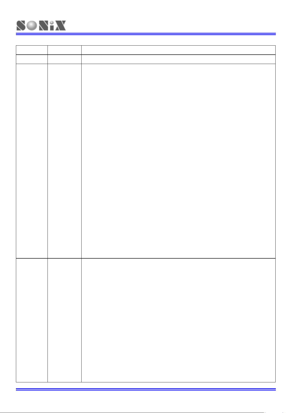
FEATURES SELECTION TABLE
Timer PWM Wakeup
CHIP ROM RAM Stack
T0 TC0 TC1
I/O ADC DAC
Buzzer
SIO
Pin no.
Package
SN8P1702 1K*16 64 - V - 12 4ch - 1 - 3
DIP18/SOP18
SN8P1704 2K*16 128 - V V 18 5ch 1ch 2 1 8 SKDIP28/SOP28
SN8P1706 V V V 30 8ch 1ch 2 1 9 DIP40
SN8P1707 V V V 33 8ch 1ch 2 1 9 QFP44
SN8P1708
4K*16 256
8
V V V 33 8ch 1ch 2 1 9 DIP48/SSOP48
Table 1-1. Selection Table of SN8P1700
MASK/OTP Relative Table
Mask Version Package Form OTP Chip for Verification Assembler Declaration
SN8A1702A DIP18/SOP18/SSOP20 SN8P1702 CHIP SN8P1702
SN8A1704A SKDIP28/SOP28 SN8P1704 CHIP SN8P1704
SN8A1706A DIP40 SN8P1706 CHIP SN8P1706
SN8A1707A QFP44 SN8P1707 CHIP SN8P1707
SN8A1708A DIP48/SSOP48 SN8P1708 CHIP SN8P1708
Note: Recommend SN8P1702A to replace SN8P1702 in new design. Refer SN8P1702A datasheet for details.
Table 1-2. MASK/OTP Relative Table
ADC GRADE TABLE
CHIP PARAMETER MIN MAX UNITS REMARK
Resolution 12 Bits
No Mission Code 8 12 Bits
SN8P170X
Differential Nonlinearity (DNL) 16 LSB
170X:
1702~1708
Resolution 12 Bits
No Mission Code 10 12 Bits
SN8P170X-12
Differential Nonlinearity (DNL) 4 LSB
170X:
1702~1708
Table 1-3. ADC Grade Table

SN8P1700
8-bit micro-controller build-in 12-bit ADC
SONiX TECHNOLOGY CO., LTD Page 12 Revision 1.94
SN8P1702 FEATURES
♦
Memory configuration
♦
Two interrupt sources
OTP ROM size: 1K * 16 bits. One internal interrupts: TC0.
RAM size: 64 * 8 bits. One external interrupts: INT0.
♦
I/O pin configuration (Total 12 pins)
♦
An 4-channel ADC with 8-bit/12-bit resolution
Input only: P0
Bi-directional: P1, P4, P5
♦
One channel PWM output. (PWM0)
Wakeup: P0, P1
♦
One channel Buzzer output. (BZ0)
Pull-up resisters: P0, P1, P4, P5
External interrupt: P0
♦
Dual clock system offers three operating modes
P4 pins shared with ADC inputs. External high clock: RC type up to 10 MHz
External high clock: Crystal type up to 16 MHz
♦
One 8-bit timer counters. (TC0).
Internal low clock: RC type 16KHz(3V), 32KHz(5V)
♦
On chip watchdog timer.
Normal mode: Both high and low clock active
♦
Eight levels stack buffer.
Slow mode: Low clock only
Sleep mode: Both high and low clock stop
♦
59 powerful instructions
Four clocks per instruction cycle
All of instructions are one word length.
♦
Package (Chip form support)
Most of instructions are one cycle only. PDIP 18 pins
All ROM area lookup table function (MOVC) SOP 18 pins / SSOP20 (MASK type only)
Notice:
1. Declare “CHIP SN8P1702” in assembler.
2. Use @SET_PUR macro to control pull-up resister. Refer I/O chapter for detailed information
3. Call @SET_PUR macro at least one time to avoid sleep mode fail.

SN8P1700
8-bit micro-controller build-in 12-bit ADC
SONiX TECHNOLOGY CO., LTD Page 13 Revision 1.94
SN8P1704 FEATURES
♦
Memory configuration
♦
Six interrupt sources
OTP ROM size: 2K * 16 bits. Three internal interrupts: TC0, TC1, SIO.
RAM size: 128 * 8 bits. Three external interrupts: INT0, INT1, INT2.
♦
I/O pin configuration (Total 18 pins)
♦
A 5-channel ADC with 8-bit/12-bit resolution.
Input only: P0
Bi-directional: P1, P4, P5
♦
One channel DAC with 7-bit resolution.
Wakeup: P0, P1
Pull-up resisters: P0, P1, P4, P5
♦
SIO function.
External interrupt: P0
♦
Two channel PWM output. (PWM0, PWM1)
P4 pins shared with ADC inputs.
♦
Two channel Buzzer output. (BZ0, BZ1)
♦
Two 8-bit timer counters. (TC0, TC1).
♦
Dual clock system offers three operating modes
♦
On chip watchdog timer.
External high clock: RC type up to 10 MHz
♦
Eight levels stack buffer.
External high clock: Crystal type up to 16 MHz
Internal low clock: RC type 16KHz(3V), 32KHz(5V)
♦
60 powerful instructions
Normal mode: Both high and low clock active
Four clocks per instruction cycle Slow mode: Low clock only
All of instructions are one word length. Sleep mode: Both high and low clock stop
Most of instructions are one cycle only.
All ROM area lookup table function (MOVC)
♦
Package (Chip form support)
Support hardware multiplier (MUL). SOP 28 pins
SKDIP 28 pins
Notice:
1. Declare “CHIP SN8P1704” in assembler.
2. Use @SET_PUR macro to control pull-up resister. Refer I/O chapter for detailed information
3. Call @SET_PUR macro at least one time to avoid sleep mode fail.

SN8P1700
8-bit micro-controller build-in 12-bit ADC
SONiX TECHNOLOGY CO., LTD Page 14 Revision 1.94
SN8P1706 FEATURES
♦
Memory configuration
♦
Seven interrupt sources
OTP ROM size: 4K * 16 bits. Four internal interrupts: T0, TC0, TC1, SIO.
RAM size: 256 * 8 bits (bank 0 and bank 1). Three external interrupts: INT0, INT1, INT2.
♦
I/O pin configuration (Total 30 pins)
♦
An 8-channel ADC with 8-bit/12-bit resolution.
Input only: P0
Bi-directional: P1, P2, P4, P5
♦
One channel DAC 7bit resolution.
Wakeup: P0, P1
Pull-up resisters: P0, P1, P2, P4, P5
External interrupt: P0
♦
SIO function.
P4 pins shared with ADC inputs.
♦
Two channel PWM output. (PWM0, PWM1)
♦
Two channel Buzzer output. (BZ0, BZ1)
♦
An 8-bit basic timer. (T0).
♦
Two 8-bit timer counters. (TC0, TC1).
♦
Dual clock system offers three operating modes
♦
On chip watchdog timer.
External high clock: RC type up to 10 MHz
♦
Eight levels stack buffer.
External high clock: Crystal type up to 16 MHz
Internal low clock: RC type 16KHz(3V), 32KHz(5V)
♦
60 powerful instructions
Normal mode: Both high and low clock active
Four clocks per instruction cycle Slow mode: Low clock only
All of instructions are one word length. Sleep mode: Both high and low clock stop
Most of instructions are one cycle only.
All ROM area lookup table function (MOVC)
Support hardware multiplier (MUL).
♦
Package (Chip form support)
P-DIP 40 pins
Notice:
1. Declare “CHIP SN8P1706” in assembler.
2. Use @SET_PUR macro to control pull-up resister. Refer I/O chapter for detailed information

SN8P1700
8-bit micro-controller build-in 12-bit ADC
SONiX TECHNOLOGY CO., LTD Page 15 Revision 1.94
SN8P1707/SN8P1708 FEATURES
♦
Memory configuration
♦
Seven interrupt sources
OTP ROM size: 4K * 16 bits. Four internal interrupts: T0, TC0, TC1, SIO.
RAM size: 256 * 8 bits (bank 0 and bank 1). Three external interrupts: INT0, INT1, INT2.
♦
I/O pin configuration (Total 33 pins)
♦
An 8-channel ADC with 8-bit/12-bit resolution.
Input only: P0
Bi-directional: P1, P2, P4, P5
♦
One channel DAC with 7-bit resolution.
Wakeup: P0, P1
Pull-up resisters: P0, P1, P2, P4, P5
External interrupt: P0
♦
SIO function.
P4 pins shared with ADC inputs.
♦
Two channel PWM output. (PWM0, PWM1)
♦
Two channel Buzzer output. (BZ0, BZ1)
♦
An 8-bit basic timer. (T0).
♦
Two 8-bit timer counters. (TC0, TC1).
♦
Dual clock system offers three operating modes
♦
On chip watchdog timer.
External high clock: RC type up to 10 MHz
♦
Eight levels stack buffer.
External high clock: Crystal type up to 16 MHz
Internal low clock: RC type 16KHz(3V), 32KHz(5V)
♦
60 powerful instructions
Normal mode: Both high and low clock active
Four clocks per instruction cycle Slow mode: Low clock only
All of instructions are one word length. Sleep mode: Both high and low clock stop
Most of instructions are one cycle only.
All ROM area lookup table function (MOVC)
Support hardware multiplier (MUL).
♦
Package (Chip form support)
QPF 44 pins (SN8P1707)
SSOP 48 pins (SN8P1708)
PDIP 48 pins (SN8P1708)
Notice:
1. Declare “CHIP SN8P1707” for SN8P1707 in assembler.
2. Declare “CHIP SN8P1708” for SN8P1708 in assembler.
3. Use @SET_PUR macro to control pull-up resister. Refer I/O chapter for detailed information

SN8P1700
8-bit micro-controller build-in 12-bit ADC
SONiX TECHNOLOGY CO., LTD Page 16 Revision 1.94
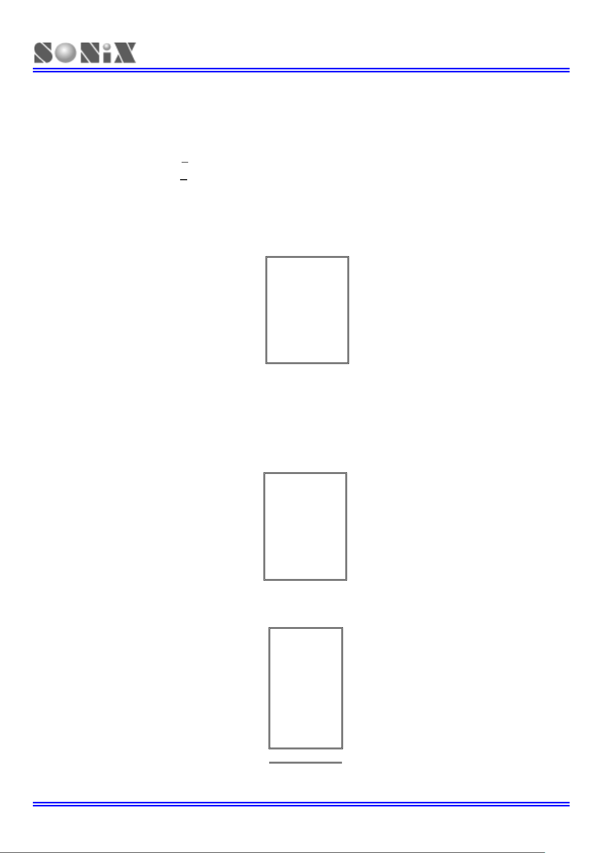
SYSTEM BLOCK DIAGRAM
Figure 1-1.Simplified System Block Diagram
PC
IR
OTP
ROM
H-OSC
TIMING GENERATOR
RAM
SYSTEM REGISTER
ALU
ACC
INTERRUPT
CONTROL
TIMER & COUNTER
PORT 0
PORT 2PORT 1 PORT 4 PORT 5
FLAGS
DAC
ADC
DAO
AIN0~AIN7
SIO
TX/RX
Internal
CLK
PWM1
PWM0
PWM0/Buzzer0
PWM1/Buzzer1
Low Volt
Detector
Watch-Dog
Timer
PC
IR
OTP
ROM
H-OSC
TIMING GENERATOR
RAM
SYSTEM REGISTER
ALU
ACC
INTERRUPT
CONTROL
TIMER & COUNTER
PORT 0
PORT 2PORT 1 PORT 4 PORT 5
FLAGS
DAC
ADC
DAO
AIN0~AIN7
SIO
TX/RX
Internal
CLK
PWM1
PWM0
PWM0/Buzzer0
PWM1/Buzzer1
Low Volt
Detector
Watch-Dog
Timer
SN8P1700
8-bit micro-controller build-in 12-bit ADC
SONiX TECHNOLOGY CO., LTD Page 17 Revision 1.94
PIN ASSIGNMENT
Format Description:SN8P17XXY
Y
= Q > QFP,P > PDIP,K > SKDIP,S > SOP,X> SSOP
OTP Type:
SN8P1702 (SOP 18PIN)
SN8P1702 (PDIP 18PIN)
P0.0/INT0 1 U 18 VDD/VPP
RST 2 17 XIN
P1.1 3 16 XOUT
P1.0 4 15 P5.0
VSS 5 14 P5.1
P4.3/AIN3 6 13 P5.2
P4.2/AIN2 7 12 P5.3
P4.1/AIN1 8 11 P5.4/BZ0/PWM0
P4.0/AIN0 9 10 VDD
SN8P1702P
SN8P1702S
MASK Type:
SN8A1702A (SOP 18PIN)
SN8A1702A (PDIP 18PIN)
SN8A1702A (SSOP 20PIN)
P0.0/INT0 1 U 18VDD
RST 2 17XIN
P1.1 3 16XOUT
P1.0 4 15P5.0
VSS 5 14P5.1
P4.3/AIN3 6 13P5.2
P4.2/AIN2 7 12P5.3
P4.1/AIN1 8 11P5.4/BZ0/PWM0
P4.0/AIN0 9 10VDD
SN8A1702AP
SN8A1702AS
VSS 1 U 20P1.0
VSS 2 19P1.1
P4.3/AIN3 3 18RST
P4.2/AIN2 4 17P0.0/INT0
P4.1/AIN1 5 16VDD
P4.0/AIN0 6 15XIN
AVREFH 7 14XOUT
VDD 8 13P5.0
P5.3 9 12P5.1
P5.2 10 11P5.4/BZ0/PWM0
SN8A1702AX
Only MASK type support SSOP20 package
SN8P1700
8-bit micro-controller build-in 12-bit ADC
SONiX TECHNOLOGY CO., LTD Page 18 Revision 1.94
OTP Type:
SN8P1704 (SOP 28PIN)
SN8P1704 (SKDIP 28PIN)
P1.4 1 U 28 RST
P1.3 2 27 P0.2/INT2
VDD 3 26 P0.1/INT1
P1.2 4 25 P0.0/INT0
P1.1 5 24 VDD/VPP
P1.0 6 23 XIN
VSS 7 22 XOUT
P4.4/AIN4 8 21 VSS
P4.3/AIN3 9 20 P5.0/SCK
P4.2/AIN2 10 19 P5.1/SI
P4.1/AIN1 11 18 P5.2/SO
P4.0/AIN0 12 17 P5.3/BZ1/PWM1
AVREFH 13 16 P5.4/BZ0/PWM0
VDD 14 15 DAO
SN8P1704K
SN8P1704S
MASK Type:
SN8A1704A (SOP 28PIN)
SN8A1704A (SKDIP 28PIN)
P1.4 1 U 28 RST
P1.3 2 27 P0.2/INT2
VDD 3 26 P0.1/INT1
P1.2 4 25 P0.0/INT0
P1.1 5 24 VDD
P1.0 6 23 XIN
VSS 7 22 XOUT
P4.4/AIN4 8 21 VSS
P4.3/AIN3 9 20 P5.0/SCK
P4.2/AIN2 10 19 P5.1/SI
P4.1/AIN1 11 18 P5.2/SO
P4.0/AIN0 12 17 P5.3/BZ1/PWM1
AVREFH 13 16 P5.4/BZ0/PWM0
VDD 14 15 DAO
SN8A1704AK
SN8A1704AS
SN8P1700
8-bit micro-controller build-in 12-bit ADC
SONiX TECHNOLOGY CO., LTD Page 19 Revision 1.94
OTP Type:
SN8P1706 (P-DIP 40PIN)
P1.5 1 U 40 RST
P1.4 2 39 P0.2/INT2
P1.3 3 38 P0.1/INT1
VDD 4 37 P0.0/INT0
P1.2 5 36 VDD/VPP
P1.1 6 35 XIN
P1.0 7 34 XOUT
P2.0 8 33 VSS
P2.1 9 32 P2.4
P2.2 10 31 P5.0/SCK
P2.3 11 30 P5.1/SI
VSS 12 29 P5.2/SO
P4.7/AIN7 13 28 P5.3/BZ1/PWM1
P4.6/AIN6 14 27 P5.4/BZ0/PWM0
P4.5/AIN5 15 26 P5.5
P4.4/AIN4 16 25 P5.6
P4.3/AIN3 17 24 P5.7
P4.2/AIN2 18 23 DAO
P4.1/AIN1 19 22 VDD
P4.0/AIN0 20 21 AVREFH
SN8P1706P
MASK Type:
SN8A1706A (P-DIP 40PIN)
P1.5 1 U 40 RST
P1.4 2 39 P0.2/INT2
P1.3 3 38 P0.1/INT1
VDD 4 37 P0.0/INT0
P1.2 5 36 NC
P1.1 6 35 XIN
P1.0 7 34 XOUT
P2.0 8 33 VSS
P2.1 9 32 P2.4
P2.2 10 31 P5.0/SCK
P2.3 11 30 P5.1/SI
AVREFL 12 29 P5.2/SO
P4.7/AIN7 13 28 P5.3/BZ1/PWM1
P4.6/AIN6 14 27 P5.4/BZ0/PWM0
P4.5/AIN5 15 26 P5.5
P4.4/AIN4 16 25 P5.6
P4.3/AIN3 17 24 P5.7
P4.2/AIN2 18 23 DAO
P4.1/AIN1 19 22 VDD
P4.0/AIN0 20 21 AVREFH
SN8A1706AP
For OTP type (SN8P1706) compatible issue, please connect AVREFL pin of MASK type (SN8A1706A) to
the analog ground of PCB. The voltage level of AVREFL pin is the valid lowest ADC input voltage. By the
way, the AVREFH is the valid highest ADC input voltage.
SN8P1700
8-bit micro-controller build-in 12-bit ADC
SONiX TECHNOLOGY CO., LTD Page 20 Revision 1.94
OTP Type:
SN8P1707 (QFP 44PIN)
XIN
XOUT
VSS
P2.7
P2.6
P2.5
P2.4
P5.0/SCK
P5.1/SI
P5.2/SO
P5.3/BZ1/PWM1
44 43 42 41 40 39 38 37 36 35 34
VPP/VDD 1
O
33 P5.4/BZ0/PWM0
P0.0/INT0 2 32 P5.5
P0.1/INT1 3 31 P5.6
P0.2/INT2 4 30 P5.7
RST 5 29 DAO
P1.5 6 SN8P1707Q 28 VDD
P1.4 7 27 AVREFH
P1.3 8 26 P4.0/AIN0
VDD 9 25 P4.1/AIN1
P1.2 10 24 P4.2/AIN2
P1.1 11 23 P4.3/AIN3
12 13 14 15 16 17 18 19 20 21 22
P1.0
P2.0
P2.1
P2.2
P2.3
VSS
AVSS
P4.7/AIN7
P4.6/AIN6
P4.5/AIN5
P4.4/AIN4
MASK Type:
SN8A1707A (QFP 44PIN)
XIN
XOUT
VSS
P2.7
P2.6
P2.5
P2.4
P5.0/SCK
P5.1/SI
P5.2/SO
P5.3/BZ1/PWM1
44 43 42 41 40 39 38 37 36 35 34
NC 1
O
33 P5.4/BZ0/PWM0
P0.0/INT0 2 32 P5.5
P0.1/INT1 3 31 P5.6
P0.2/INT2 4 30 P5.7
RST 5 29 DAO
P1.5 6 SN8A1707AQ 28 VDD
P1.4 7 27 AVREFH
P1.3 8 26 P4.0/AIN0
VDD 9 25 P4.1/AIN1
P1.2 10 24 P4.2/AIN2
P1.1 11 23 P4.3/AIN3
12 13 14 15 16 17 18 19 20 21 22
P1.0
P2.0
P2.1
P2.2
P2.3
VSS
AVREFL
P4.7/AIN7
P4.6/AIN6
P4.5/AIN5
P4.4/AIN4
For OTP type (SN8P1707) compatible issue, please connect AVREFL pin of MASK type (SN8A1707A) to
the analog ground of PCB. The voltage level of AVREFL pin is the valid lowest ADC input voltage. By the
way, the AVREFH is the valid highest ADC input voltage.
SN8P1700
8-bit micro-controller build-in 12-bit ADC
SONiX TECHNOLOGY CO., LTD Page 21 Revision 1.94
OTP Type:
SN8P1708 (SSOP 48PIN)
SN8P1708 (P-DIP 48PIN)
P2.5 1 U 48 P2.4
P2.6 2 47 P5.0/SCK
P2.7 3 46 P5.1/SI
VSS 4 45 P5.2/SO
VSS 5 44 P5.3/BZ1/PWM1
XOUT 6 43 VSS
XIN 7 42 P5.4/BZ0/PWM0
VPP/VDD 8 41 P5.5
P0.0/INT0 9 40 P5.6
P0.1/INT1 10 39 P5.7
P0.2/INT2 11 38 DAO
RST 12 37 VDD
P1.5 13 36 AVDD
P1.4 14 35 AVREFH
P1.3 15 34 P4.0/AIN0
VDD 16 33 P4.1/AIN1
VSS 17 32 P4.2/AIN2
P1.2 18 31 P4.3/AIN3
P1.1 19 30 P4.4/AIN4
P1.0 20 29 P4.5/AIN5
P2.0 21 28 P4.6/AIN6
P2.1 22 27 P4.7/AIN7
P2.2 23 26 AVSS
P2.3 24 25 VSS
SN8P1708P
SN8P1708X
MASK Type:
SN8A1708A (SSOP 48PIN)
SN8A1708A (P-DIP 48PIN)
P2.5 1 U 48 P2.4
P2.6 2 47 P5.0/SCK
P2.7 3 46 P5.1/SI
VSS 4 45 P5.2/SO
VSS 5 44 P5.3/BZ1/PWM1
XOUT 6 43 VSS
XIN 7 42 P5.4/BZ0/PWM0
NC 8 41 P5.5
P0.0/INT0 9 40 P5.6
P0.1/INT1 10 39 P5.7
P0.2/INT2 11 38 DAO
RST 12 37 VDD
P1.5 13 36 AVDD
P1.4 14 35 AVREFH
P1.3 15 34 P4.0/AIN0
VDD 16 33 P4.1/AIN1
VSS 17 32 P4.2/AIN2
P1.2 18 31 P4.3/AIN3
P1.1 19 30 P4.4/AIN4
P1.0 20 29 P4.5/AIN5
P2.0 21 28 P4.6/AIN6
P2.1 22 27 P4.7/AIN7
P2.2 23 26 AVREFL
P2.3 24 25 VSS
SN8A1708AP
SN8A1708AX
For OTP type (SN8P1708) compatible issue, please connect AVREFL pin of MASK type (SN8A1708A) to
the analog ground of PCB. The voltage level of AVREFL pin is the valid lowest ADC input voltage. By the
way, the AVREFH is the valid highest ADC input voltage.
SN8P1700
8-bit micro-controller build-in 12-bit ADC
SONiX TECHNOLOGY CO., LTD Page 22 Revision 1.94
PIN DESCRIPTIONS
PIN NAME TYPE DESCRIPTION
VDD, VSS P Power supply input pins for digital circuit.
AVDD, AVSS P Power supply input pins for analog circuit.
VPP/VDD P OTP ROM programming pin. Connect to VDD in normal operation.
RST I System reset input pin. Schmitt trigger structure, active “low”, normal stay to “high”.
XIN, XOUT I, O External oscillator pins. RC mode from XIN.
P0.0 / INT0 I Port 0.0 and shared with INT0 trigger pin (Schmitt trigger) / Built-in pull-up resisters.
P0.1 / INT1 I Port 0.1 and shared with INT1 trigger pin (Schmitt trigger) / Built-in pull-up resisters.
P0.2 / INT2 I Port 0.2 and shared with INT2 trigger pin (Schmitt trigger) / Built-in pull-up resisters.
P1.0 ~ P1.5 I/O Port 1.0~Port 1.5 bi-direction pins / Built-in pull-up resisters.
P2.0 ~ P2.7 I/O Port 2.0~Port 2.7 bi-direction pins / Built-in pull-up resisters.
P4.0 ~ P4.7 I/O Port 4.0~Port 4.7 bi-direction pins / Built-in pull-up resisters.
P5.0 / SCK I/O Port 5.0 bi-direction pin and SIO’s clock input/output / Built-in pull-up resisters.
P5.1 / SI I/O Port 5.1 bi-direction pin and SIO’s data input / Built-in pull-up resisters.
P5.2 / SO I/O Port 5.2 bi-direction pin and SIO’s data output / Built-in pull-up resisters.
P5.3 / BZ1 / PWM1 I/O
Port 5.3 bi-direction pin, TC1 ÷ 2 signal output pin for buzzer or PWM1 output pin.
Built-in pull-up resisters.
P5.4 / BZ0 / PWM0 I/O
Port 5.4 bi-direction pin, TC0 ÷ 2 signal output pin for buzzer or PWM0 output pin.
Built-in pull-up resisters.
P5.5 ~ P5.7 I/O Port 5.5~Port 5.7 bi-direction pins / Built-in pull-up resisters.
AVREFH I A/D converter high analog reference voltage.
AIN0 ~ AIN7 I Analog signal input pins for ADC converter.
DAO O 5-bit DAC signal output pin.
Table 1-4. SN8P1700 Pin Description
PIN CIRCUIT DIAGRAMS
Figure 1-2. Pin Circuit Diagram
Note: All of the latch output circuits are push-pull structures.
Po rt0 stru ctu re
PUR
Pin
Int. bus
PUR
PnM
Pin
Int. bus
PnM
Latch
Port1, 2, 4, 5 structure
PnM
Po rt0 stru ctu re
PUR
Pin
Int. bus
PUR
PnM
Pin
Int. bus
PnM
Latch
Port1, 2, 4, 5 structure
PnM
SN8P1700
8-bit micro-controller build-in 12-bit ADC
SONiX TECHNOLOGY CO., LTD Page 23 Revision 1.94
2
2
2
CODE OPTION TABLE
Code Option Content Function Description
RC Low cost RC for external high clock oscillator
32K X’tal
Low frequency, power saving crystal (e.g. 32.768K) for external high
clock oscillator
12M X’tal High speed crystal /resonator (e.g. 12M) for external high clock oscillator
High_Clk
4M X’tal Standard crystal /resonator (e.g. 3.58M) for external high clock oscillator
Enable External high clock divided by two, Fosc = high clock / 2
High_Clk / 2
Disable Fosc = high clock
Enable Enable Oscillator Safe Guard function
OSG
Disable Disable Oscillator Safe Guard function
Enable Enable Watch Dog function
Watch_Dog
Disable Disable Watch Dog function
Enable Enable the low voltage detect
LVD
Disable Disable the low voltage detect
Enable Enable ROM code Security function
Security
Disable Disable ROM code Security function
Table 2-1. Code Option Table of SN8P1700
Notice : The OSG working voltage and the frequency relation table:
The min. working voltage will be affect by the OSG option. It is very important to check this code option.
Turn on the OSG will improve the EMI performance. But the side effect is an increase in the working
voltage.
OSC. Freq.(Mhz)
OSG ON (Volt) OSG OFF(Volt)
1 2.4 2.2
2 2.4 2.2
4 2.5 2.2
6 2.5 2.3
8 2.6 2.4
10 2.8 2.6
12 3 2.7
16 3.5 2.8
18 3.7 3
20 4.1 3.2
Notice : The system working frequency is only warranty under 16Mhz.
SN8P1700
8-bit micro-controller build-in 12-bit ADC
SONiX TECHNOLOGY CO., LTD Page 24 Revision 1.94
3
3
3
ADDRESS SPACES
PROGRAM MEMORY (ROM)
OVERVIEW
ROM Maps for SN8P1700 devices provide OTP memory that programmable by user. SN8P1702 has 1K x 16-bit
program memory, SN8P1704 has 2K x 16-bit program memory and SN8P1706, SN8P1707 and SN8P1708 have 4K x
16-bit program memory. The SN8P1700 program memory is able to fetch instructions through 12-bit wide PC
(Program Counter) and can look up ROM data by using ROM code registers (R, X, Y, Z). In standard configuration, the
device’s 4,096 x 16-bit program memory has four areas:
1-word reset vector addresses
1-word Interrupt vector addresses
5-words reserved area
4K words (SN8P1706, SN8P1707, SN8P1708)
2K words (SN8P1704)
1K words (SN8P1702)
All of the program memory is partitioned into three coding areas. The 1
st
area is located from 00H to 03H(The Reset
vector area), the 2
nd
area is a reserved area 04H ~07H, the 3rd area is for the interrupt vector and the user code area
from 0008H to 0FFEH. The address 08H is the interrupt enter address point.
ROM
0000H
Reset vector
User reset vector
0001H Jump to user start address
0002H Jump to user start address
0003H
General purpose area
Jump to user start address
0004H
0005H
0006H
0007H
Reserved
0008H
Interrupt vector
User interrupt vector
0009H User program
.
.
000FH
0010H
0011H
.
.
03FEH
General purpose area
End of user program
03FFH
Reserved
Figure 3-1. ROM Address Structure (SN8P1702)
SN8P1700
8-bit micro-controller build-in 12-bit ADC
SONiX TECHNOLOGY CO., LTD Page 25 Revision 1.94
ROM
0000H
Reset vector
User reset vector
0001H Jump to user start address
0002H Jump to user start address
0003H
General purpose area
Jump to user start address
0004H
0005H
0006H
0007H
Reserved
0008H
Interrupt vector
User interrupt vector
0009H User program
.
.
000FH
0010H
0011H
.
.
07FEH
General purpose area
End of user program
07FFH
Reserved
Figure 3-2. ROM Address Structure (SN8P1704)
ROM
0000H
Reset vector
User reset vector
0001H Jump to user start address
0002H Jump to user start address
0003H
General purpose area
Jump to user start address
0004H
0005H
0006H
0007H
Reserved
0008H
Interrupt vector
User interrupt vector
0009H User program
.
.
000FH
0010H
0011H
.
.
0FFEH
General purpose area
End of user program
0FFFH
Reserved
Figure 3-3. ROM Address Structure (SN8P1706/SN8P1707/SN8P1708)

SN8P1700
8-bit micro-controller build-in 12-bit ADC
SONiX TECHNOLOGY CO., LTD Page 26 Revision 1.94
USER RESET VECTOR ADDRESS (0000H)
A 1-word vector address area is used to execute system reset. After power on reset or watchdog timer overflow reset,
then the chip will restart the program from address 0000h and all system registers will be set as default values. The
following example shows the way to define the reset vector in the program memory.
Example: After power on reset, external reset active or reset by watchdog timer overflow.
CHIP SN8P1708
ORG 0 ; 0000H
JMP START ; Jump to user program address.
. ; 0001H ~ 0007H are reserved
ORG 10H
START: ; 0010H, The head of user program.
. ; User program
.
.
.
ENDP
; End of program
INTERRUPT VECTOR ADDRESS (0008H)
A 1-word vector address area is used to execute interrupt request. If any interrupt service is executed, the program
counter (PC) value is stored in stack buffer and points to 0008h of program memory to execute the vectored interrupt.
Users have to define the interrupt vector. The following example shows the way to define the interrupt vector in the
program memory.
Example 1: This demo program includes interrupt service routine and the user program is behind the
interrupt service routine.
CHIP SN8P1708
ORG 0 ; 0000H
JMP START ; Jump to user program address.
. ; 0001H ~ 0007H are reserved
ORG 8
; Interrupt service routine
B0XCH A, ACCBUF
; B0XCH doesn’t change C, Z flag
PUSH
; Push 80H ~ 87H system registers
.
.
.
POP
; Pop 80H ~ 87H system registers
B0XCH A, ACCBUF
RETI
; End of interrupt service routine
START: ; The head of user program.
.
; User program
.
.
.
JMP START
; End of user program
ENDP
; End of program

SN8P1700
8-bit micro-controller build-in 12-bit ADC
SONiX TECHNOLOGY CO., LTD Page 27 Revision 1.94
Example 2: The demo program includes interrupt service routine and the address of interrupt service
routine is in a special address of general-purpose area.
CHIP SN8P1708
ORG 0 ; 0000H
JMP START ; Jump to user program address.
. ; 0001H ~ 0007H are reserved
ORG 08
JMP MY_IRQ ; 0008H, Jump to interrupt service routine address
ORG 10H
START: ; 0010H, The head of user program.
. ; User program
.
.
.
JMP START
; End of user program
MY_IRQ: ;The head of interrupt service routine
B0XCH A, ACCBUF
; B0XCH doesn’t change C, Z flag
PUSH
; Push 80H ~ 87H system registers
.
.
.
POP
; Pop 80H ~ 87H system registers
B0XCH A, ACCBUF
RETI
; End of interrupt service routine
ENDP
; End of program
Remark: It is easy to get the rules of SONIX program from demo programs given above. These points are
as following.
1. The address 0000H is a “JMP” instruction to make the program go to general-purpose ROM area. The
0004H~0007H are reserved. Users have to skip 0004H~0007H addresses. It is very important and
necessary.
2. The interrupt service starts from 0008H. Users can put the whole interrupt service routine from 0008H
(Example1) or to put a “JMP” instruction in 0008H then place the interrupt service routine in other
general-purpose ROM area (Example2) to get more modularized coding style.

SN8P1700
8-bit micro-controller build-in 12-bit ADC
SONiX TECHNOLOGY CO., LTD Page 28 Revision 1.94
CHECKSUM CALCULATION
The ROM addresses 0004H~0007H and last address are reserved area. User should avoid these addresses
(0004H~0007H and last address) when calculate the Checksum value.
Example:
The demo program shows how to avoid 0004H~0007H when calculated Checksum from 00H to the end of
user’s code
MOV A,#END_USER_CODE$L
B0MOV END_ADDR1,A ;save low end address to end_addr1
MOV A,#END_USER_CODE$M
B0MOV END_ADDR2,A ;save middle end address to end_addr2
CLR Y ;set Y to ooH
CLR Z ;set Z to 00H
@@:
CALL YZ_CHECK ;call function of check yz value
MOVC ;
B0BSET FC ;clear C glag
ADD DATA1,A ;add A to Data1
MOV A,R
ADC DATA2,A ;add R to Data2
JMP END_CHECK ;check if the YZ address = the end of code
AAA:
INCMS Z ;Z=Z+1
JMP @B ;if Z!= 00H calculate to next address
JMP Y_ADD_1 ;if Z=00H increase Y
END_CHECK:
MOV A,END_ADDR1
CMPRS A,Z ;check if Z = low end address
JMP AAA ;if Not jump to checksum calculate
MOV A,END_ADDR2
CMPRS A,Y ;if Yes, check if Y = middle end address
JMP AAA ;if Not jump to checksum calculate
JMP CHECKSUM_END ;if Yes checksum calculated is done.
YZ_CHECK: ;check if YZ=0004H
MOV A,#04H
CMPRS A,Z ;check if Z=04H
RET ;if Not return to checksum calculate
MOV A,#00H
CMPRS A,Y ;if Yes, check if Y=00H
RET ;if Not return to checksum calculate
INCMS Z ;if Yes, increase 4 to Z
INCMS Z
INCMS Z
INCMS Z
RET ;set YZ=0008H then return
Y_ADD_1:
INCMS Y ;increase Y
NOP
JMP @B ;jump to checksum calculate
CHECKSUM_END:
……….
……….
END_USER_CODE: ;Label of program end

SN8P1700
8-bit micro-controller build-in 12-bit ADC
SONiX TECHNOLOGY CO., LTD Page 29 Revision 1.94
GENERAL PURPOSE PROGRAM MEMORY AREA
The 4089
1
-word at ROM locations 0010H~0FFEH are used as general-purpose memory. The area is stored
instruction’s op-code and look-up table data. The SN8P1700 includes jump table function by using program counter
(PC) and look-up table function by using ROM code registers (R, X, Y, Z).
The boundary of program memory is separated by the high-byte program counter (PCH) every 100H. In jump table
function and look-up table function, the program counter can’t leap over the boundary by program counter
automatically. Users need to modify the PCH value to “PCH+1” as the PCL overflow (from 0FFH to 000H).
Notice: 1:The SN8P1702’s ROM size is about 1K words and the SN8P1704’s ROM size is about 2K words.
LOOKUP TABLE DESCRIPTION
In the ROM’s data lookup function, the X register is pointed to the highest 8-bit, Y register to the middle 8-bit and Z
register to the lowest 8-bit data of ROM address. After MOVC instruction is executed, the low-byte data of ROM then
will be stored in ACC and high-byte data stored in R register.
Example: To look up the ROM data located “TABLE1”.
B0MOV Y, #TABLE1$M ; To set lookup table1’s middle address
B0MOV Z, #TABLE1$L ; To set lookup table1’s low address.
MOVC ; To lookup data, R = 00H, ACC = 35H
;
; Increment the index address for next address
INCMS Z ; Z+1
JMP @F ; Not overflow
INCMS Y ; Z overflow (FFH 00), Y=Y+1
NOP ; Not overflow
;
@@:
MOVC ; To lookup data, R = 51H, ACC = 05H.
. . ;
TABLE1: DW 0035H ; To define a word (16 bits) data.
DW 5105H ; “
DW 2012H ; “
CAUSION: The Y register can't increase automatically if Z register cross boundary from 0xFF to 0x00.
Therefore, user must take care such situation to avoid loop-up table errors. If Z register overflow, Y
register must be added one. The following INC_YZ macro shows a simple method to process Y and Z
registers automatically.
Note: Because the program counter (PC) is only 12-bit, the X register is useless in the application. Users
can omit “B0MOV X, #TABLE1$H”. SONiX ICE support more larger program memory addressing
capability. So make sure X register is “0” to avoid unpredicted error in loop-up table operation.
Example: INC_YZ Macro
INC_YZ MACRO
INCMS Z ; Z+1
JMP @F ; Not overflow
INCMS Y ; Y+1
NOP ; Not overflow
@@:
ENDM

SN8P1700
8-bit micro-controller build-in 12-bit ADC
SONiX TECHNOLOGY CO., LTD Page 30 Revision 1.94
The other coding style of loop-up table is to add Y or Z index register by accumulator. Be careful if carry happen. Refer
following example for detailed information:
Example: Increase Y and Z register by B0ADD/ADD instruction
B0MOV Y, #TABLE1$M ; To set lookup table’s middle address.
B0MOV Z, #TABLE1$L ; To set lookup table’s low address.
B0MOV A, BUF ; Z = Z + BUF.
B0ADD Z, A
B0BTS1 FC ; Check the carry flag.
JMP GETDATA ; FC = 0
INCMS Y ; FC = 1. Y+1.
NOP
GETDATA: ;
MOVC ; To lookup data. If BUF = 0, data is 0x0035
; If BUF = 1, data is 0x5105
; If BUF = 2, data is 0x2012
.
.
. . ;
TABLE1: DW 0035H ; To define a word (16 bits) data.
DW 5105H ; “
DW 2012H ; “
 Loading...