

SONIX SN8P1702BP, SN8P1702BS, SN8P1702BX Datasheet
Preliminary SN8P1702A/SN8P1703A
8-bit micro-controller build-in 12-bit ADC
SONiX TECHNOLOGY CO., LTD Page 1 Revision 0.5
*-
SN8P1700A Series
USER’S MANUAL
Preliminary
SN8P1702A
SN8P1703A
S
S
O
O
N
Nii
X
X 88--
B
Biitt
M
Miiccrroo--
C
Coonnttrroolllleerr
SONIX reserves the right to make change without further notice to any products herein to improve reliability, function or design. SONIX does not
assume any liability arising out of the application or use of any product or circuit described herein; neither does it convey any license under its patent
rights nor the rights of others. SONIX products are not designed, intended, or authorized for us as components in systems intended, for surgical
implant into the body, or other applications intended to support or sustain life, or for any other application in which the fai lure of the SONIX product
could create a situation where personal injury or death may occur. Should Buyer purchase or use SONIX products for any such unintended or
unauthorized application. Buyer shall indemnify and hold SONIX and its officers, employees, subsidiaries, affiliates and distributors harmless against
all claims, cost, damages, and expenses, and reasonable attorney fees arising out of, directly or indirectly, any claim of pe rsonal injury or death
associated with such unintended or unauthorized use even if such claim alleges that SONIX was negligent regarding the design or manufacture of
the part.
Preliminary SN8P1702A/SN8P1703A
8-bit micro-controller build-in 12-bit ADC
SONiX TECHNOLOGY CO., LTD Page 2 Revision 0.5
AMENDMENT HISTORY
Version Date Description
VER 0.1 Jul. 2003 V1.0 Preliminary Version
VER 0.2 Jul. 2003 Change watchdog overflow table
VER 0.3 Jul. 2003
Aug. 2003
1. Modify selection table
2. DC current chars. Change
3. Feature change
4. Change SN8P1703 part number to SN8P1703A
5. Code option table has been relocated after pin description section.
6. Modify QTP approval sheet
7. Change Register description.
8. Add LVD typical value=1.8V in Elec. Char.
9. Add “Noise Filter” code option
VER 0.4 Sep. 2003 1. Add SN8P1702A SSOP20 for Mask Mass production.
2. Add TC1 Timer in Update table.
3. Modify Chap. 8 table/figure no.
4. Modify TC0/TC1 timer description and table.
5. Modify PWM description and table.
6. Modify electrical characteristic table
VER 0.5 Sep. 2003 1. Modify ADC convert time table
2. Modify the description of PEDGE register.
3. Modify the description of INTRQ register.
3. Remove approval sheet.
4. Separate the pin description section of SN8P1702A and SN8P1703A.
5. Remove PCB layout section
6. Add P-DIP 20 and Sop 20 package information.
7. Add SN8A1702B and SN8A1703A related description.

Preliminary SN8P1702A/SN8P1703A
8-bit micro-controller build-in 12-bit ADC
SONiX TECHNOLOGY CO., LTD Page 3 Revision 0.5
Table of Contents
AMENDMENT HISTORY.............................................................................................................. 2
1
1
1
PRODUCT OVERVIEW..................................................................................................... 8
GENERAL DESCRIPTION ........................................................................................................... 8
FEATURES SELECTION TABLE................................................................................................. 8
MASK/OTP RELATIVE TABLE.......................................................................................................... 8
ADC GRADE TABLE .................................................................................................................... 8
UPGRADE FROM SN8P1702 (OLD VERSION OTP)....................................................................... 9
SN8P1702A/SN8P1703A FEATURES ....................................................................................... 10
SYSTEM BLOCK DIAGRAM ...................................................................................................... 11
PIN ASSIGNMENT..................................................................................................................... 12
SN8P1702A Pin Assignment................................................................................................... 12
SN8P1703A Pin Assignment................................................................................................... 14
PIN DESCRIPTIONS.................................................................................................................. 15
PIN CIRCUIT DIAGRAMS .......................................................................................................... 15
2
2
2
CODE OPTION TABLE................................................................................................... 16
3
3
3
ADDRESS SPACES........................................................................................................ 17
PROGRAM MEMORY (ROM)..................................................................................................... 17
OVERVIEW............................................................................................................................. 17
USER RESET VECTOR ADDRESS (0000H) ......................................................................... 18
INTERRUPT VECTOR ADDRESS (0008H)............................................................................ 18
CHECKSUM CALCULATION.................................................................................................. 20
GENERAL PURPOSE PROGRAM MEMORY AREA ............................................................. 21
LOOKUP TABLE DESCRIPTION............................................................................................ 21
JUMP TABLE DESCRIPTION................................................................................................. 23
DATA MEMORY (RAM).............................................................................................................. 25

Preliminary SN8P1702A/SN8P1703A
8-bit micro-controller build-in 12-bit ADC
SONiX TECHNOLOGY CO., LTD Page 4 Revision 0.5
OVERVIEW............................................................................................................................. 25
WORKING REGISTERS............................................................................................................. 26
Y, Z REGISTERS.................................................................................................................... 26
R REGISTERS........................................................................................................................ 27
PROGRAM FLAG....................................................................................................................... 27
CARRY FLAG ......................................................................................................................... 27
DECIMAL CARRY FLAG......................................................................................................... 27
ZERO FLAG............................................................................................................................ 27
ACCUMULATOR........................................................................................................................ 28
STACK OPERATIONS................................................................................................................29
OVERVIEW............................................................................................................................. 29
STACK REGISTERS............................................................................................................... 30
STACK OPERATION EXAMPLE ............................................................................................ 31
PROGRAM COUNTER............................................................................................................... 32
ONE ADDRESS SKIPPING .................................................................................................... 33
MULTI-ADDRESS JUMPING.................................................................................................. 34
4
4
4
ADDRESSING MODE...................................................................................................... 35
OVERVIEW................................................................................................................................. 35
IMMEDIATE ADDRESSING MODE........................................................................................ 35
DIRECTLY ADDRESSING MODE.......................................................................................... 35
INDIRECTLY ADDRESSING MODE....................................................................................... 35
TO ACCESS DATA in RAM BANK 0....................................................................................... 36
5
5
5
SYSTEM REGISTER....................................................................................................... 37
OVERVIEW................................................................................................................................. 37
SYSTEM REGISTER ARRANGEMENT (BANK 0)..................................................................... 37
BYTES of SYSTEM REGISTER.............................................................................................. 37
BITS of SYSTEM REGISTER ................................................................................................. 38
6
6
6
POWER ON RESET ........................................................................................................ 39

Preliminary SN8P1702A/SN8P1703A
8-bit micro-controller build-in 12-bit ADC
SONiX TECHNOLOGY CO., LTD Page 5 Revision 0.5
OVERVIEW................................................................................................................................. 39
EXTERNAL RESET DESCRIPTION........................................................................................... 40
7
7
7
OSCILLATORS................................................................................................................ 42
OVERVIEW................................................................................................................................. 42
CLOCK BLOCK DIAGRAM..................................................................................................... 42
OSCM REGISTER DESCRIPTION......................................................................................... 43
EXTERNAL HIGH-SPEED OSCILLATOR............................................................................... 44
OSCILLATOR MODE CODE OPTION.................................................................................... 44
OSCILLATOR DEVIDE BY 2 CODE OPTION......................................................................... 44
OSCILLATOR SAFE GUARD CODE OPTION ....................................................................... 44
SYSTEM OSCILLATOR CIRCUITS........................................................................................ 45
External RC Oscillator Frequency Measurement .................................................................... 46
INTERNAL LOW-SPEED OSCILLATOR.................................................................................... 47
SYSTEM MODE DESCRIPTION................................................................................................ 48
OVERVIEW............................................................................................................................. 48
NORMAL MODE.....................................................................................................................48
SLOW MODE.......................................................................................................................... 48
GREEN MODE........................................................................................................................ 48
POWER DOWN MODE........................................................................................................... 48
SYSTEM MODE CONTROL....................................................................................................... 49
SYSTEM MODE BLOCK DIAGRAM....................................................................................... 49
SYSTEM MODE SWITCHING ................................................................................................ 50
WAKEUP TIME........................................................................................................................... 51
OVERVIEW............................................................................................................................. 51
HARDWARE WAKEUP........................................................................................................... 51
EXTERNAL WAKEUP TRIGGER CONTROL......................................................................... 52
8
8
8
TIMERS COUNTERS....................................................................................................... 53
WATCHDOG TIMER (WDT)....................................................................................................... 53
T0M REGISTER............................................................................................................................. 54
TIMER COUNTER 0 (TC0)......................................................................................................... 55
OVERVIEW............................................................................................................................. 55
TC0M MODE REGISTER........................................................................................................ 56

Preliminary SN8P1702A/SN8P1703A
8-bit micro-controller build-in 12-bit ADC
SONiX TECHNOLOGY CO., LTD Page 6 Revision 0.5
TC0C COUNTING REGISTER................................................................................................ 57
TC0 Overflow Time ................................................................................................................. 57
TC0R AUTO-LOAD REGISTER.............................................................................................. 60
TC0 TIMER COUNTER OPERATION SEQUENCE................................................................ 61
TC0 CLOCK FREQUENCY OUTPUT (BUZZER) ................................................................... 63
TC0OUT FREQUENCY TABLE.................................................................................................. 64
TIMER COUNTER 1 (TC1)......................................................................................................... 66
OVERVIEW............................................................................................................................. 66
TC1M MODE REGISTER........................................................................................................ 67
TC1C COUNTING REGISTER................................................................................................ 68
TC1 Overflow Time ................................................................................................................. 68
TC1R AUTO-LOAD REGISTER.............................................................................................. 71
TC1 TIMER COUNTER OPERATION SEQUENCE................................................................ 72
TC1 CLOCK FREQUENCY OUTPUT (BUZZER) ................................................................... 74
PWM FUNCTION DESCRIPTION.............................................................................................. 75
OVERVIEW............................................................................................................................. 75
PWM PROGRAM DESCRIPTION........................................................................................... 78
9
9
9
INTERRUPT..................................................................................................................... 79
OVERVIEW................................................................................................................................. 79
INTEN INTERRUPT ENABLE REGISTER ................................................................................. 80
INTRQ INTERRUPT REQUEST REGISTER.............................................................................. 80
INTERRUPT OPERATION DESCRIPTION................................................................................ 81
GIE GLOBAL INTERRUPT OPERATION ............................................................................... 81
INT0 (P0.0) INTERRUPT OPERATION .................................................................................. 82
TC0 INTERRUPT OPERATION.............................................................................................. 83
TC1 INTERRUPT OPERATION.............................................................................................. 84
MULTI-INTERRUPT OPERATION.......................................................................................... 85
1
1
1
0
0
0
I/O PORT............................................................................................................... 87
OVERVIEW................................................................................................................................. 87
I/O PORT FUNCTION TABLE .................................................................................................... 88
PULL-UP RESISTERS................................................................................................................ 89
I/O PORT DATA REGISTER ...................................................................................................... 92

Preliminary SN8P1702A/SN8P1703A
8-bit micro-controller build-in 12-bit ADC
SONiX TECHNOLOGY CO., LTD Page 7 Revision 0.5
1
1
1
1
1
1
4-CHANNEL ANALOG TO DIGITAL CONVERTER............................................. 94
OVERVIEW................................................................................................................................. 94
ADM REGISTER......................................................................................................................... 95
ADR REGISTERS....................................................................................................................... 95
ADB REGISTERS....................................................................................................................... 96
P4CON REGISTERS.................................................................................................................. 97
ADC CONVERTING TIME.......................................................................................................... 98
ADC CIRCUIT............................................................................................................................. 99
1
1
1
2
2
2
CODING ISSUE .................................................................................................. 100
TEMPLATE CODE.................................................................................................................... 100
PROGRAM CHECK LIST ......................................................................................................... 104
1
1
1
3
3
3
INSTRUCTION SET TABLE ............................................................................... 105
1
1
1
4
4
4
ELECTRICAL CHARACTERISTIC..................................................................... 106
ABSOLUTE MAXIMUM RATING.............................................................................................. 106
STANDARD ELECTRICAL CHARACTERISTIC....................................................................... 106
1
1
1
5
5
5
PACKAGE INFORMATION ................................................................................ 107
P-DIP18 PIN ............................................................................................................................. 107
SOP18 PIN ............................................................................................................................... 108
P-DIP 20 PIN ............................................................................................................................ 109
SOP 20 PIN .............................................................................................................................. 110
SSOP20 PIN............................................................................................................................. 111
Preliminary SN8P1702A/SN8P1703A
8-bit micro-controller build-in 12-bit ADC
SONiX TECHNOLOGY CO., LTD Page 8 Revision 0.5
1
1
1
PRODUCT OVERVIEW
GENERAL DESCRIPTION
The SN8P1702A/SN8P1703A is a series of 8-bit micro-controller. This chip is utilized with CMOS technology
fabrication and featured with low power consumption and high performance by its unique electronic structure.
This chip is designed with the excellent IC structure including the large program memory OTP ROM, the massive data
memory RAM, two 8-bit timer counters (TC0, TC1), a watchdog timer, three interrupt sources (TC0, TC1, INT0), an
4-channel ADC converter with 8-bit/12-bit resolution, two channels high speed PWM output (PWM0, PWM1), two
channels buzzer output (BZ0, BZ1) and 8-level stack buffers.
Besides, the user can choose desired oscillator configurations for the controller. There are four oscillator configurations
to select for generating system clock, including High/Low Speed crystal, ceramic resonator or cost-saving RC. This
series also includes an internal RC oscillator for slow mode controlled by programming.
FEATURES SELECTION TABLE
Timer PWM Wakeup
CHIP ROM RAM Stack
T0 TC0 TC1
I/O AVref ADC
Buzzer Pin no.
Package
SN8P1702A 1K*16 128 - V V 12 - 4ch 2 3
DIP18/SOP18/SSOP20
SN8P1703A 1K*16 128
8
- V V 13 V 4ch 2 3
DIP20/SOP20/SSOP20
Table 1-1. Selection Table of SN8P1702A/SN8P1703A
MASK/OTP Relative Table
MASK Part Number Package Form
OTP Chip for Verification
Assembler Declaration
SN8A1702A DIP18/SOP18 /SSOP20 SN8P1702A CHIP SN8P1702A
SN8A1702B DIP18/SOP18 /SSOP20 SN8P1702A CHIP SN8P1702AOTP
SN8A1703A DIP20/SOP20 /SSOP20 SN8P1703A CHIP SN8P1703A
ADC GRADE TABLE
CHIP PARAMETER MIN MAX UNITS
Resolution 12 Bits
No Mission Code 8 12 Bits
SN8P1702A
SN8P1703A
Differential No linearity (DNL) 16 LSB
Resolution 12 Bits
No Mission Code 10 12 Bits
SN8P1702A-12
SN8P1703A-12
Differential No linearity (DNL) 4 LSB
Table 1-2. ADC Grade Table
Preliminary SN8P1702A/SN8P1703A
8-bit micro-controller build-in 12-bit ADC
SONiX TECHNOLOGY CO., LTD Page 9 Revision 0.5
UPGRADE FROM SN8P1702 (Old version OTP)
Chip SN8P1702 SN8P1702A SN8P1702A SN8P1703A
Assembly Declaration CHIP SN8P1702 CHIP SN8P1702A CHIP SN8P1702AOTP CHIP SN8P1703A
Standby current (3V) 3uA < 1uA < 1uA < 1uA
4MHz Operating (3V) 1.5mA < 1mA < 1mA < 1mA
4MHz Operating (5V) 7mA < 3mA < 3mA < 3mA
Green Mode - Yes Yes Yes
P0.0 Interrupt Edge Falling Falling/Rising/Both Falling/Rising/Both Falling/Rising/Both
P1 wake up Low Level Level change Level change Level change
AVREFH NO Only SSOP20 Only SSOP20 Yes
ADC Channel 4 4 4 4
P4CON register - - Yes Yes
RAM size 64 64 128 128
GPIO 12 12 12 13
TC1 Timer - - Yes Yes
Fast PWM - - Yes Yes
Pull-up Resistor By Port By Port By Pin By Pin
Pull-up Register @SET_PUR @SET_PUR PnUR PnUR
SN8P1702 Pin
Compatible
Yes Yes Yes No
WDT clock source High Clock High Clock
High Clock
Internal RC
High Clock
Internal RC
Internal RC always ON
and WDT clock source
fixed at internal RC
- - Yes Yes
Power On Delay
at 4MHz/3V
~70ms ~200ms ~200ms ~200ms
MASK Type SN8A1702A SN8A1702A SN8A1702B SN8A1703A
Package
PDIP18/SOP18 PDIP18/SOP18/SSOP20 PDIP18/SOP18/SSOP20 PDIP20/SOP20/SSOP20
Notice: The SN8P1702 is not recommended for the new design.

Preliminary SN8P1702A/SN8P1703A
8-bit micro-controller build-in 12-bit ADC
SONiX TECHNOLOGY CO., LTD Page 10 Revision 0.5
SN8P1702A/SN8P1703A FEATURES
♦
Memory configuration
♦
Three interrupt sources
OTP ROM size: 1K * 16 bits. Two internal interrupts: TC0, TC1
RAM size: 128 * 8 bits. One external interrupts: INT0.
♦
I/O pin configuration
♦
An 4-channel 12-bit ADC
Input only: P0
Bi-directional: P1, P4, P5
♦
Two channel high speed PWM output.
Wakeup: P0, P1
♦
Two channel Buzzer output. (BZ0/BZ1)
Pull-up resisters: P0, P1, P4, P5
External interrupt: P0
♦
Dual clock system offers four operating modes
P4 pins shared with ADC inputs. External high clock: RC type up to 10 MHz
External high clock: Crystal type up to 16 MHz
♦
Two 8-bit timer counters. (TC0, TC1).
Internal low clock: RC type 16KHz(3V), 32KHz(5V)
♦
On chip watchdog timer.
Normal mode: Both high and internal low cloc k active
♦
Eight levels stack buffer.
Slow mode: Internal low clock only
Green mode: Periodical wake-up by timer
Sleep mode: Both high and internal low clock stop
♦
59 powerful instructions
Four clocks per instruction cycle
All of instructions are one word length.
♦
Package (Chip form support)
Most of instructions are one cycle only. SN8P1702A -- PDIP 18 / SOP 18 / SSOP20
All ROM area lookup table function (MOVC) SN8P1703A-- PDIP 20 / SOP 20 / SSOP20
Preliminary SN8P1702A/SN8P1703A
8-bit micro-controller build-in 12-bit ADC
SONiX TECHNOLOGY CO., LTD Page 11 Revision 0.5
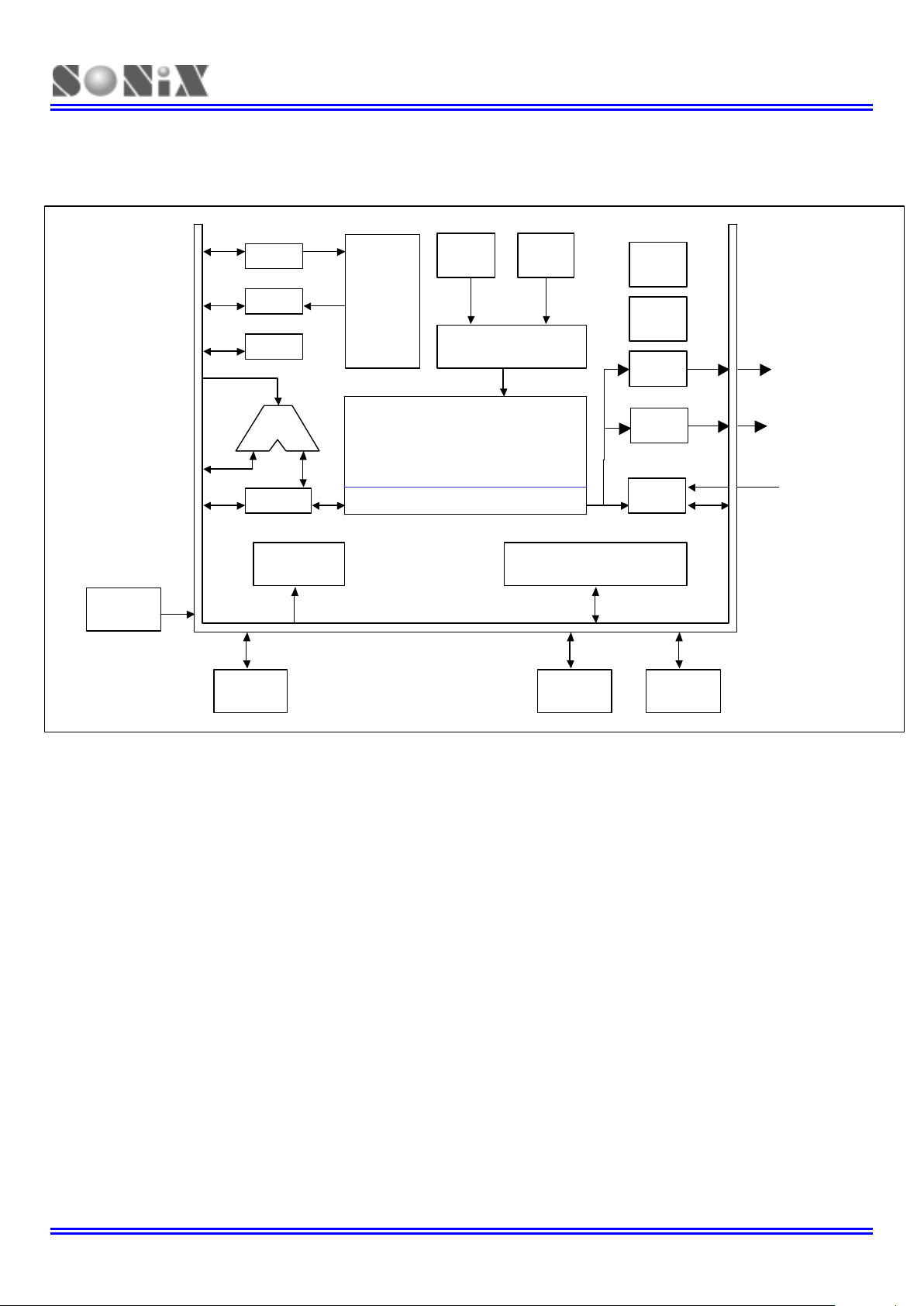
SYSTEM BLOCK DIAGRAM
Figure 1-1.Simplified System Block Diagram
PC
IR
OTP
ROM
H-OSC
TIMIN G GENERATOR
RAM
S YSTEM R E GIST E R
ALU
ACC
INTERRUPT
CONT ROL
TIME R & COUNTER
PORT 0
PO RT 1 PORT 4 PO RT 5
FLAGS
ADC
AIN0~AIN3
Internal
CLK
PWM0
PWM0/Buzzer0
Low Volt
Dete ctor
Watch-Dog
Timer
PWM1
PWM1/Buzzer1
Preliminary SN8P1702A/SN8P1703A
8-bit micro-controller build-in 12-bit ADC
SONiX TECHNOLOGY CO., LTD Page 12 Revision 0.5
PIN ASSIGNMENT
Format Description:SN8P170XAY
Y
= P > PDIP, S > SOP,X> SSOP
SN8P1702A Pin Assignment
OTP Type:
SN8P1702AS (SOP 18PIN) / SN8P1702AP (PDIP 18PIN)
Pin compatible to the MASK version (SN8A1702AS/SN8A1702AP)
P0.0/INT0 1 U 18 VDD
RST 2 17 XIN
P1.1 3 16 XOUT
P1.0 4 15 P5.0
VSS 5 14 P5.1
P4.3/AIN3 6 13 P5.2
P4.2/AIN2 7 12 P5.3/BZ1/PWM1
P4.1/AIN1 8 11 P5.4/BZ0/PWM0
P4.0/AIN0 9 10 VDD
SN8P1702AP
SN8P1702AS
SN8P1702AX (SSOP 20PIN)
Pin compatible to the MASK version (SN8A1702AX)
VSS 1 U 20 P1.0
VSS 2 19 P1.1
P4.3/AIN2 3 18 RST
P4.2/AIN1 4 17 P0.0/INT0
P4.1/AIN1 5 16 VDD
P4.0/AIN0 6 15 XIN
AVREFH 7 14 XOUT
VDD 8 13 P5.0
P5.3/BZ1/PWM1 9 12 P5.1
P5.2 10 11 P5.4/BZ0/PWM0
SN8P1702AX
OLD Version OTP Type:
SN8P1702S (SOP 18PIN) / SN8P1702P (PDIP 18PIN)
P0.0/INT0 1 U 18 VDD/VPP
RST 2 17 XIN
P1.1 3 16 XOUT
P1.0 4 15 P5.0
VSS 5 14 P5.1
P4.3/AIN3 6 13 P5.2
P4.2/AIN2 7 12 P5.3/BZ1/PWM1
P4.1/AIN1 8 11 P5.4/BZ0/PWM0
P4.0/AIN0 9 10 VDD
SN8P1702P
SN8P1702S
Notice: The SN8P1702 is not recommended for the new design.
Preliminary SN8P1702A/SN8P1703A
8-bit micro-controller build-in 12-bit ADC
SONiX TECHNOLOGY CO., LTD Page 13 Revision 0.5
MASK Type:
SN8A1702AS (SOP 18PIN) / SN8A1702AP (PDIP 18PIN)
SN8A1702BS (SOP 18PIN) / SN8A1702BP (PDIP 18PIN)
P0.0/INT0 1 U 18 VDD
RST 2 17 XIN
P1.1 3 16 XOUT
P1.0 4 15 P5.0
VSS 5 14 P5.1
P4.3/AIN3 6 13 P5.2
P4.2/AIN2 7 12 P5.3
P4.1/AIN1 8 11 P5.4/BZ0/PWM0
P4.0/AIN0 9 10 VDD
SN8A1702AP
SN8A1702AS
SN8A1702BP
SN8A1702BS
SN8A1702AX (SSOP 20PIN)
VSS 1 U 20 P1.0
VSS 2 19 P1.1
P4.3/AIN2 3 18 RST
P4.2/AIN1 4 17 P0.0/INT0
P4.1/AIN1 5 16 VDD
P4.0/AIN0 6 15 XIN
AVREFH 7 14 XOUT
VDD 8 13 P5.0
P5.3 9 12 P5.1
P5.2 10 11 P5.4/BZ0/PWM0
SN8A1702AX
SN8A1702BX

Preliminary SN8P1702A/SN8P1703A
8-bit micro-controller build-in 12-bit ADC
SONiX TECHNOLOGY CO., LTD Page 14 Revision 0.5
SN8P1703A Pin Assignment
OTP Type:
SN8P1703AS (SOP 20PIN) / SN8P1703AP (PDIP 20PIN) / SN8P1703AX (SSOP 20PIN)
P0.0/INT0 1 U 20 VDD
RST 2 19 XIN
P1.1 3 18 XOUT
P1.0 4 17 P5.0
VSS 5 16 P5.1
P4.3/AIN3 6 15 P5.2
P4.2/AIN2 7 14 P5.3/BZ1/PWM1
P4.1/AIN1 8 13 P5.4/BZ0/PWM0
P4.0/AIN0 9 12 P5.5
AVREFH 10 11 VDD
SN8P1703AP
SN8P1703AS
SN8P1703AX
MASK Type:
SN8A1703AS (SOP 20PIN) / SN8A1703AP (PDIP 20PIN) / SN8A1703AX (SSOP 20PIN)
P0.0/INT0 1 U 20 VDD
RST 2 19 XIN
P1.1 3 18 XOUT
P1.0 4 17 P5.0
VSS 5 16 P5.1
P4.3/AIN3 6 15 P5.2
P4.2/AIN2 7 14 P5.3/BZ1/PWM1
P4.1/AIN1 8 13 P5.4/BZ0/PWM0
P4.0/AIN0 9 12 P5.5
AVREFH 10 11 VDD
SN8A1703AP
SN8A1703AS
SN8A1703AX

Preliminary SN8P1702A/SN8P1703A
8-bit micro-controller build-in 12-bit ADC
SONiX TECHNOLOGY CO., LTD Page 15 Revision 0.5
PIN DESCRIPTIONS
PIN NAME TYPE DESCRIPTION
VDD, VSS P Power supply input pins for digital circuit.
RST I System reset input pin. Schmitt trigger structure, active “low”, normal stay to “high”.
XIN, XOUT I, O External oscillator pins. RC mode from XIN.
P0.0 / INT0 I Port 0.0 and shared with INT0 trigger pin (Schmitt trigger) / Built-in pull-up resisters.
P1.0 ~ P1.1 I/O Port 1.0~Port 1.1 bi-direction pins / Built-in pull-up resisters.
P4.0 ~ P4.3 I/O Port 4.0~Port 4.3 bi-direction pins / Built-in pull-up resisters.
P5.0~P5.2, P5.5 I/O Port 5.0~Port 5.2, P5.5 bi-direction pins / Built-in pull-up resisters.
P5.3 / BZ1 / PWM1 I/O
Port 5.3 bi-direction pin, TC1÷2 signal output pin for buzzer or PWM1 output pin.
Built-in pull-up resisters.
P5.4 / BZ0 / PWM0 I/O
Port 5.4 bi-direction pin, TC0÷2 signal output pin for buzzer or PWM0 output pin.
Built-in pull-up resisters.
AVREFH I A/D converter high analog reference voltage.
AIN0 ~ AIN3 I Analog signal input pins for ADC converter.
Table 1-3. Pin Description
PIN CIRCUIT DIAGRAMS
Figure 1-2. Pin Circuit Diagram
Note: All of the latch output circuits are push-pull structures.
Port0 structure
PUR
Pin
Int. bus
PUR
PnM
Pin
Int. bus
PnM
Latch
Port1, 4, 5 structure
PnM
Port0 structure
PUR
Pin
Int. bus
PUR
PnM
Pin
Int. bus
PnM
Latch
Port1, 4, 5 structure
PnM
Preliminary SN8P1702A/SN8P1703A
8-bit micro-controller build-in 12-bit ADC
SONiX TECHNOLOGY CO., LTD Page 16 Revision 0.5
2
2
2
CODE OPTION TABLE
Code Option Content Function Description
RC Low cost RC for external high clock oscillator
32K X’tal
Low frequency, power saving crystal (e.g. 32.768K) for external high
clock oscillator
12M X’tal High speed crystal /resonator (e.g. 12M) for external high clock oscillator
High_Clk
4M X’tal Standard crystal /resonator (e.g. 3.58M) for external high clock oscillator
Enable External high clock divided by two, Fosc = high clock / 2
High_Clk / 2
Disable Fosc = hi gh clock
Enable Enable Oscillator Safe Guard function
OSG
Disable Disable Os cillator Safe Guard function
Enable Enable Watch Dog function
Watch_Dog
Disable Disable Watch Dog function
Enable Enable ROM code Security function
Security
Disable Disable ROM code Security function
8-bit TC0 as 8-bit counter.
6-bit TC0 as 6-bit counter.
5-bit TC0 as 5-bit counter.
TC0_Counter
4-bit TC0 as 4-bit counter.
8-bit TC1 as 8-bit counter.
6-bit TC1 as 6-bit counter.
5-bit TC1 as 5-bit counter.
TC1_Counter
4-bit TC1 as 4-bit counter.
Enable Enable Noise Filter function to enhance EMI performance
Noise Filter
Disable Disable Noise Filter function
Enable Enable Low Power function to save Operating current
Low Power
Disable Disable Low Power function
Always ON
Force Watch Dog Timer clock source come from INT 16K RC.
Also INT 16K RC never stop both in power down and green mode that
means Watch Dog Timer will always enable both in power down and
green mode.
INT_16K_RC
By_CPUM Enable or Disable internal 16K(at 3V) RC clock by CPUM registe r
Table 2-1. Code Option Table of SN8P1702A/SN8P1703A
Notice:
In high noisy environment, enable “Noise Filter”, “OSG” and disable “Low Power” is strongly
recommended.
The side effect is to increase the lowest valid working voltage level if enable “Noise Filter” or
“OSG” or “Low Power” code option.
Enable “Low Power” option will reduce operating current except in 32K X’tal or slow mode.
If users select “32K X’tal” in “High_Clk” option, assembler will force “OSG” to be enabled.
If users select “RC” in “High_Clk” option, assembler will force “High_Clk / 2” to be enabled.
Preliminary SN8P1702A/SN8P1703A
8-bit micro-controller build-in 12-bit ADC
SONiX TECHNOLOGY CO., LTD Page 17 Revision 0.5
3
3
3
ADDRESS SPACES
PROGRAM MEMORY (ROM)
OVERVIEW
ROM Maps for SN8P1702A/SN8P1703A devices provide 1K x 16-bit program memory. The SN8P1702A/SN8P1703A
program memory is able to fetch instructions through 12-bit wide PC (Program Counter) and can look up ROM data by
using ROM code registers (R, X, Y, Z). In standard configuration, the device’s 1,024 x 16-bit program memory has four
areas:
1-word reset vector addresses
1-word Interrupt vector addresses
5-words reserved area
1K words (SN8P1702)
All of the program memory is partitioned into three coding areas. The first area is located from 00H to 03H(The Reset
vector area), the second area is a reserved area 04H ~07H, the third area is for the interrupt vector and the user code
area from 0008H to 03FEH. The address 08H is the interrupt enter address point.
ROM
0000H
Reset vector
User reset vector
0001H Jump to user start address
0002H Jump to user start address
0003H
General purpose area
Jump to user start address
0004H
0005H
0006H
0007H
Reserved
0008H
Interrupt vector
User interrupt vector
0009H User program
.
.
000FH
0010H
0011H
.
.
03FEH
General purpose area
End of user program
03FFH
Reserved
Figure 3-1. ROM Address Structure

Preliminary SN8P1702A/SN8P1703A
8-bit micro-controller build-in 12-bit ADC
SONiX TECHNOLOGY CO., LTD Page 18 Revision 0.5
USER RESET VECTOR ADDRESS (0000H)
A 1-word vector address area is used to execute system reset. After power on reset or watchdog timer overflow reset,
then the chip will restart the program from address 0000h and all system registers will be set as default values. The
following example shows the way to define the reset vector in the program memory.
Example: After power on reset, external reset active or reset by watchdog timer overflow.
CHIP SN8P1702A
ORG 0 ; 0000H
JMP START ; Jump to user program address.
. ; 0001H ~ 0007H are reserved
ORG 10H
START: ; 0010H, The head of user program.
. ; User program
.
.
.
ENDP
; End of program
INTERRUPT VECTOR ADDRESS (0008H)
A 1-word vector address area is used to execute interrupt request. If any interrupt service is executed, the program
counter (PC) value is stored in stack buffer and points to 0008h of program memory to execute the vectored interrupt.
Users have to define the interrupt vector. The following example shows the way to define the interrupt vector in the
program memory.
Example 1: This demo program includes interrupt service routine and the user program is behind the
interrupt service routine.
CHIP SN8P1702A
ORG 0 ; 0000H
JMP START ; Jump to user program address.
. ; 0001H ~ 0007H are reserved
ORG 8
; Interrupt service routine
B0XCH A, ACCBUF
; B0XCH doesn’t change C, Z flag
B0MOV A, PFLAG
B0MOV PFLAGBUF, A
; Save PFLAG register in a buffer
.
.
.
B0MOV A, PFLAGBUF
B0MOV PFLAG, A
; Restore PFLAG register from buffer
B0XCH A, ACCBUF
; B0XCH doesn’t change C, Z flag
RETI
; End of interrupt service routine
START: ; The head of user program.
.
; User program
.
.
.
JMP START
; End of user program
ENDP
; End of program

Preliminary SN8P1702A/SN8P1703A
8-bit micro-controller build-in 12-bit ADC
SONiX TECHNOLOGY CO., LTD Page 19 Revision 0.5
Example 2: The demo program includes interrupt service routine and the address of interrupt service
routine is in a special address of general-purpose area.
CHIP SN8P1702A
ORG 0 ; 0000H
JMP START ; Jump to user program address.
. ; 0001H ~ 0007H are reserved
ORG 08
JMP MY_IRQ ; 0008H, Jump to interrupt service routine address
ORG 10H
START: ; 0010H, The head of user program.
. ; User program
.
.
.
JMP START
; End of user program
MY_IRQ: ; The head of interrupt service routine
B0XCH A, ACCBUF
; B0XCH doesn’t change C, Z flag
B0MOV A, PFLAG
B0MOV PFLAGBUF, A
; Save PFLAG register in a buffer
.
.
.
B0MOV A, PFLAGBUF
B0MOV PFLAG, A
; Restore PFLAG register from buffer
B0XCH A, ACCBUF
; B0XCH doesn’t change C, Z flag
RETI
; End of interrupt service routine
ENDP
; End of program
Remark: It is easy to get the rules of SONIX program from demo programs given above. These points are
as following.
1. The address 0000H is a “JMP” instruction to make the program go to general-purpose ROM area. The
0004H~0007H are reserved. Users have to skip 0004H~0007H addresses. It is very important and
necessary.
2. The interrupt service starts from 0008H. Users can put the whole interrupt service routine from 0008H
(Example1) or to put a “JMP” instruction in 0008H then place the interrupt service routine in other
general-purpose ROM area (Example2) to get more modularized coding style.

Preliminary SN8P1702A/SN8P1703A
8-bit micro-controller build-in 12-bit ADC
SONiX TECHNOLOGY CO., LTD Page 20 Revision 0.5
CHECKSUM CALCULATION
The ROM addresses 0004H~0007H and last address are reserved area. User should avoid these addresses
(0004H~0007H and last address) when calculate the Checksum value.
Example:
The demo program shows how to avoid 0004H~0007H when calculated Checksum from 00H to the end of
user’s code
MOV A,#END_USER_CODE$L
B0MOV END_ADDR1,A ; save low end address to end_addr1
MOV A,#END_USER_CODE$M
B0MOV END_ADDR2,A ; Save middle end address to end_addr2
CLR Y ; Set Y to 00H
CLR Z ; Set Z to 00H
@@:
CALL YZ_CHECK ; Call function of check yz value
MOVC ;
B0BSET FC ; Clear C flag
ADD DATA1,A ; Add A to Data1
MOV A,R
ADC DATA2,A ; Add R to Data2
JMP END_CHECK ; Check if the YZ address = the end of code
AAA:
INCMS Z ;Z=Z+1
JMP @B ; If Z! = 00H calculate to next address
JMP Y_ADD_1 ; If Z=00H increase Y
END_CHECK:
MOV A,END_ADDR1
CMPRS A,Z ; Check if Z = low end address
JMP AAA ; If Not jump to checksum calculate
MOV A,END_ADDR2
CMPRS A,Y ; If Yes, check if Y = middle end address
JMP AAA ; If Not jump to checksum calculate
JMP CHECKSUM_END ; If Yes checksum calculated is done.
YZ_CHECK: ;check if YZ=0004H
MOV A,#04H
CMPRS A,Z ;check if Z=04H
RET ;if Not return to checksum calculate
MOV A,#00H
CMPRS A,Y ;if Yes, check if Y=00H
RET ;if Not return to checksum calculate
INCMS Z ;if Yes, increase 4 to Z
INCMS Z
INCMS Z
INCMS Z
RET ;set YZ=0008H then return
Y_ADD_1:
INCMS Y ;increase Y
NOP
JMP @B ;jump to checksum calculate
CHECKSUM_END:
……….
……….
END_USER_CODE: ;Label of program end

Preliminary SN8P1702A/SN8P1703A
8-bit micro-controller build-in 12-bit ADC
SONiX TECHNOLOGY CO., LTD Page 21 Revision 0.5
GENERAL PURPOSE PROGRAM MEMORY AREA
The 992-word at ROM locations 0010H~0FEFH are used as general-purpose memory. The area is stored instruction’s
op-code and look-up table data. The SN8P1702A/SN8P1703A includes jump table function by using program counter
(PC) and look-up table function by using ROM code registers (R, X, Y, Z).
The boundary of program memory is separated by the high-byte program counter (PCH) every 100H. In jump table
function and look-up table function, the program counter can’t leap over the boundary by program counter
automatically. Users need to modify the PCH value to “PCH+1” as the PCL overflow (from 0FFH to 000H).
LOOKUP TABLE DESCRIPTION
In the ROM’s data lookup function, the X register is pointed to the highest 8-bit, Y register to the middle 8-bit and Z
register to the lowest 8-bit data of ROM address. After MOVC instruction is executed, the low-byte data of ROM then
will be stored in ACC and high-byte data stored in R register.
Example: To look up the ROM data located “TABLE1”.
B0MOV Y, #TABLE1$M ; To set lookup table1’s middle address
B0MOV Z, #TABLE1$L ; To set lookup table1’s low address.
MOVC ; To lookup data, R = 00H, ACC = 35H
;
; Increment the index address for next address
INCMS Z ; Z+1
JMP @F ; Not overflow
INCMS Y ; Z overflow (FFH 00), Y=Y+1
NOP ; Not overflow
;
@@: MOVC ; To lookup data, R = 51H, ACC = 05H.
. . ;
TABLE1: DW 0035H ; To define a word (16 bits) data.
DW 5105H ; “
DW 2012H ; “
CAUSION: The Y register can't increase automatically if Z register cross boundary from 0xFF to 0x00.
Therefore, user must take care such situation to avoid loop-up table errors. If Z register overflow, Y
register must be added one. The following INC_YZ macro shows a simple method to process Y and Z
registers automatically.
Note: Because the program counter (PC) is only 12-bit, the X register is useless in the application. Users
can omit “B0MOV X, #TABLE1$H”. SONiX ICE support more larger program memory addressing
capability. So make sure X register is “0” to avoid unpredicted error in loop-up table operation.
Example: INC_YZ Macro
INC_YZ MACRO
INCMS Z ; Z+1
JMP @F ; Not overflow
INCMS Y ; Y+1
NOP ; Not overflow
@@:
ENDM

Preliminary SN8P1702A/SN8P1703A
8-bit micro-controller build-in 12-bit ADC
SONiX TECHNOLOGY CO., LTD Page 22 Revision 0.5
The other coding style of loop-up table is to add Y or Z index register by accumulator. Be careful if carry happen. Refer
following example for detailed information:
Example: Increase Y and Z register by B0ADD/ADD instruction
B0MOV Y, #TABLE1$M ; To set lookup table’s middle address.
B0MOV Z, #TABLE1$L ; To set lookup table’s low address
B0MOV A, BUF ; Z = Z + BUF.
B0ADD Z, A
B0BTS1 FC ; Check the carry flag.
JMP GETDATA ; FC = 0
INCMS Y ; FC = 1. Y+1.
NOP
GETDATA: ;
MOVC ; To lookup data. If BUF = 0, data is 0x0035
; If BUF = 1, data is 0x5105
; If BUF = 2, data is 0x2012
.
.
. . ;
TABLE1: DW 0035H ; To define a word (16 bits) data.
DW 5105H ; “
DW 2012H ; “

Preliminary SN8P1702A/SN8P1703A
8-bit micro-controller build-in 12-bit ADC
SONiX TECHNOLOGY CO., LTD Page 23 Revision 0.5
JUMP TABLE DESCRIPTION
The jump table operation is one of multi-address jumping function. Add low-byte program counter (PCL) and ACC
value to get one new PCL. The new program counter (PC) points to a series jump instructions as a listing table. The
way is easy to make a multi-stage program.
When carry flag occurs after executing of “ADD PCL, A”, it will not affect PCH register. Users have to check if the jump
table leaps over the ROM page boundary or the listing file generated by SONIX assembly software. If the jump table
leaps over the ROM page boundary (e.g. from xxFFH to xx00H), move the jump table to the top of next program
memory page (xx00H). Here one page mean 256 words.
Example : If PC = 0323H (PCH = 03H、PCL = 23H)
ORG 0X0100 ; The jump table is from the head of the ROM boundary
B0ADD PCL, A ; PCL = PCL + ACC, the PCH can’t be changed.
JMP A0POINT ; ACC = 0, jump to A0POINT
JMP A1POINT ; ACC = 1, jump to A1POINT
JMP A2POINT ; ACC = 2, jump to A2POINT
JMP A3POINT ; ACC = 3, jump to A3POINT
In following example, the jump table starts at 0x00FD. When execute B0ADD PCL, A. If ACC = 0 or 1, the jump
table points to the right address. If the ACC is larger then 1 will cause error because PCH doesn't increase one
automatically. We can see the PCL = 0 when ACC = 2 but the PCH still keep in 0. The program counter (PC) will
point to a wrong address 0x0000 and crash system operation. It is important to check whether the jump table
crosses over the boundary (xxFFH to xx00H). A good coding style is to put the jump table at the start of ROM
boundary (e.g. 0100H).
Example: If “jump table” crosses over ROM boundary will cause errors.
ROM Address
. .
. .
. .
0X00FD
B0ADD PCL, A ; PCL = PCL + ACC, the PCH can’t be changed.
0X00FE
JMP A0POINT ; ACC = 0
0X00FF
JMP A1POINT ; ACC = 1
0X0100
JMP A2POINT ; ACC = 2 jump table cross boundary here
0X0101
JMP A3POINT ; ACC = 3
. .
. .
SONIX provides a macro for safe jump table function. This macro will check the ROM boundary and move the jump
table to the right position automatically. The side effect of this macro is maybe wasting some ROM size. Notice the
maximum jump table number for this macro is limited fewer than 254.
@JMP_A MACRO VAL
IF (($+1) !& 0XFF00) !!= (($+(VAL)) !& 0XFF00)
JMP ($ | 0XFF)
ORG ($ | 0XFF)
ENDIF
ADD PCL, A
ENDM
Note: “VAL” is the number of the jump table listing number.

Preliminary SN8P1702A/SN8P1703A
8-bit micro-controller build-in 12-bit ADC
SONiX TECHNOLOGY CO., LTD Page 24 Revision 0.5
Example: “@JMP_A” application in SONIX macro file called “MACRO3.H”.
B0MOV A, BUF0 ; “BUF0” is from 0 to 4.
@JMP_A 5 ; The number of the jump table listing is five.
JMP A0POINT ; If ACC = 0, jump to A0POINT
JMP A1POINT ; ACC = 1, jump to A1POINT
JMP A2POINT ; ACC = 2, jump to A2POINT
JMP A3POINT ; ACC = 3, jump to A3POINT
JMP A4POINT ; ACC = 4, jump to A4POINT
If the jump table position is from 00FDH to 0101H, the “@JMP_A” macro will make the jump table to start from 0100h.
Preliminary SN8P1702A/SN8P1703A
8-bit micro-controller build-in 12-bit ADC
SONiX TECHNOLOGY CO., LTD Page 25 Revision 0.5
DATA MEMORY (RAM)
OVERVIEW
The SN8P1702A/SN8P1703A has internally built-in the data memory up to 256 bytes for storing the general-purpose
data.
128 * 8-bit general purpose area in bank 0
128 * 8-bit system special register area
The memory is separated into bank 0 and bank 1. The user can program RAM bank selection bits of RBANK register to
access all data in any of the two RAM banks. The bank 0, using the first 128-byte location assigned as
general-purpose area, and the remaining 128-byte in bank 0 as system register.
RAM location
000h 000h~07Fh of Bank 0 = To store general-
“ purpose data (128 bytes).
“
“
“
“
07Fh
General purpose area
080h 080h~0FFh of Bank 0 = To store system
“ registers (128 bytes).
“
“
“
“
System register
BANK 0
0FFh
End of bank 0 area
Figure 3-2. RAM Location
Note: The undefined locations of system register area are logic “high” after executing read instruction
“MOV A, M”.

Preliminary SN8P1702A/SN8P1703A
8-bit micro-controller build-in 12-bit ADC
SONiX TECHNOLOGY CO., LTD Page 26 Revision 0.5
WORKING REGISTERS
The locations 82H to 84H of RAM bank 0 in data memory stores the specially defined registers such as register R, Z, Y,
respectively shown in the following table. These registers can use as the general purpose of working buffer and be
used to access ROM’s and RAM’s data. For instance, all of the ROM’s table can be looked-up with R, Y and Z
registers. The data of RAM memory can be indirectly accessed with Y and Z registers.
82H 83H 84H
RAM
R Z Y
R/W R/W R/W
Y, Z REGISTERS
The Y and Z registers are the 8-bit buffers. There are three major functions of these registers. First, Y and Z registers
can be used as working registers. Second, these two registers can be used as data pointers for @YZ register. Third,
the registers can be address ROM location in order to look-up RO M data.
Y initial value = 0000 0000
084H Bit 7 Bit 6 Bit 5 Bit 4 Bit 3 Bit 2 Bit 1 Bit 0
Y
YBIT7 YBIT6 YBIT5 YBIT4 YBIT3 YBIT2 YBIT1 YBIT0
R/W R/W R/W R/W R/W R/W R/W R/W
Z initial value = 0000 0000
083H Bit 7 Bit 6 Bit 5 Bit 4 Bit 3 Bit 2 Bit 1 Bit 0
Z
ZBIT7 ZBIT6 ZBIT5 ZBIT4 ZBIT3 ZBIT2 ZBIT1 ZBIT0
R/W R/W R/W R/W R/W R/W R/W R/W
The @YZ that is data point_1 index buffer located at address E7H in RAM bank 0. It employs Y and Z registers to
addressing RAM location in order to read/write data through ACC. The Lower 4-bit of Y register is pointed to RAM bank
number and Z register is pointed to RAM address number, respectively. The higher 4-bit data of Y register is truncated
in RAM indirectly access mode.
Example: If want to read a data from RAM address 25H of bank 1, it can use indirectly addressing mode to
access data as following.
B0MOV Y, #01H ; To set RAM bank 1 for Y register
B0MOV Z, #25H ; To set location 25H for Z register
B0MOV A, @YZ ; To read a data into ACC
Example: Clear general-purpose data memory area of bank 1 using @YZ register.
MOV A, #1
B0MOV Y, A ; Y = 1, bank 1
MOV A, #07FH
B0MOV Z, A ; Y = 7FH, the last address of the data memory area
CLR_YZ_BUF:
CLR @YZ ; Clear @YZ to be zero
DECMS Z ; Y – 1, if Y= 0, finish the routine
JMP CLR_YZ_BUF ; Not zero
CLR @YZ
END_CLR: ; End of clear general purpose data memory area of bank 0
Note: Please consult the “LOOK-UP TABLE DESCRIPTION” about Y, Z register look-up table application.
Preliminary SN8P1702A/SN8P1703A
8-bit micro-controller build-in 12-bit ADC
SONiX TECHNOLOGY CO., LTD Page 27 Revision 0.5
R REGISTERS
There are two major functions of the R register. First, R register can be used as working registers. Second, the R
registers can be store high-byte data of look-up ROM data. After MOVC instruction executed, the high-byte data of a
ROM address will be stored in R register and the low-byte data stored in ACC.
R initial value = 0000 0000
082H Bit 7 Bit 6 Bit 5 Bit 4 Bit 3 Bit 2 Bit 1 Bit 0
R
RBIT7 RBIT6 RBIT5 RBIT4 RBIT3 RBIT2 RBIT1 RBIT0
R/W R/W R/W R/W R/W R/W R/W R/W
Note: Please consult the “LOOK-UP TABLE DESCRIPTION” about R register look-up table application.
PROGRAM FLAG
The PFLAG includes carry flag (C), decimal carry flag (DC) and zero flag (Z). If the result of operating is zero or there is
carry, borrow occurrence, then these flags will be set to PFLAG register.
PFLAG initial value = xxxx x000
086H Bit 7 Bit 6 Bit 5 Bit 4 Bit 3 Bit 2 Bit 1 Bit 0
PFLAG
- - - - - C DC Z
- - - - - R/W R/W R/W
CARRY FLAG
C = 1: If executed arithmetic addition with occurring carry signal or executed arithmetic subtraction without borrowing
signal or executed rotation instruction with shifting out logic “1”.
C = 0: If executed arithmetic addition without occurring carry signal or executed arithmetic subtraction with borrowing
signal or executed rotation instruction with shifting out logic “0”.
DECIMAL CARRY FLAG
DC = 1: If executed arithmetic addition with occurring carry signal from low nibble or executed arithmetic subtraction
without borrow signal from high nibble.
DC = 0: If executed arithmetic addition without occurring carry signal from low nibble or executed arithmetic subtraction
with borrow signal from high nibble.
ZERO FLAG
Z = 1: After operation, the content of ACC is zero.
Z = 0: After operation, the content of ACC is not zero.

Preliminary SN8P1702A/SN8P1703A
8-bit micro-controller build-in 12-bit ADC
SONiX TECHNOLOGY CO., LTD Page 28 Revision 0.5
ACCUMULATOR
The ACC is an 8-bits data register responsible for transferring or manipulating data between ALU and data memory. If
the result of operating is zero (Z) or there is carry (C or DC) occurrence, then these flags will be set to PFLAG register.
ACC is not in data memory (RAM), so ACC can’t be access by “B0MOV” instruction during the instant addressing
mode.
Example: Read and write ACC value.
; Read ACC data and store in BUF data memory
MOV BUF, A
. .
; Write a immediate data into ACC
MOV A, #0FH
. .
; Write ACC data from BUF data memory
MOV A, BUF
. .
The system doesn’t store ACC and PFLAG value as any interrupt service executed. ACC must be exchanged to
another data memory defined by users. Thus, once interrupt occurs, these data must be stored in the data memory
based on the user’s program as follows.
Example: ACC and working registers protection.
ACCBUF EQU 00H ; ACCBUF is ACC data buffer in bank 0.
INT_SERVICE:
B0XCH A, ACCBUF
; B0XCH doesn’t change C, Z flag
B0XCH A, ACCBUF ; Store ACC value
B0MOV A, PFLAG ; Store PFLAG value
B0MOV PFLAGBUF,A
.
B0MOV A, PFLAGBUF ; Re-load PFLAG value
B0MOV PFLAG,A
B0XCH A, ACCBUF ; Re-load ACC
B0XCH A, ACCBUF ; Re-load ACC
RETI ; Exit interrupt service vector
Notice: To save and re-load ACC data must be used “B0XCH” instruction, or the PLAGE value maybe
modified by ACC.
Preliminary SN8P1702A/SN8P1703A
8-bit micro-controller build-in 12-bit ADC
SONiX TECHNOLOGY CO., LTD Page 29 Revision 0.5
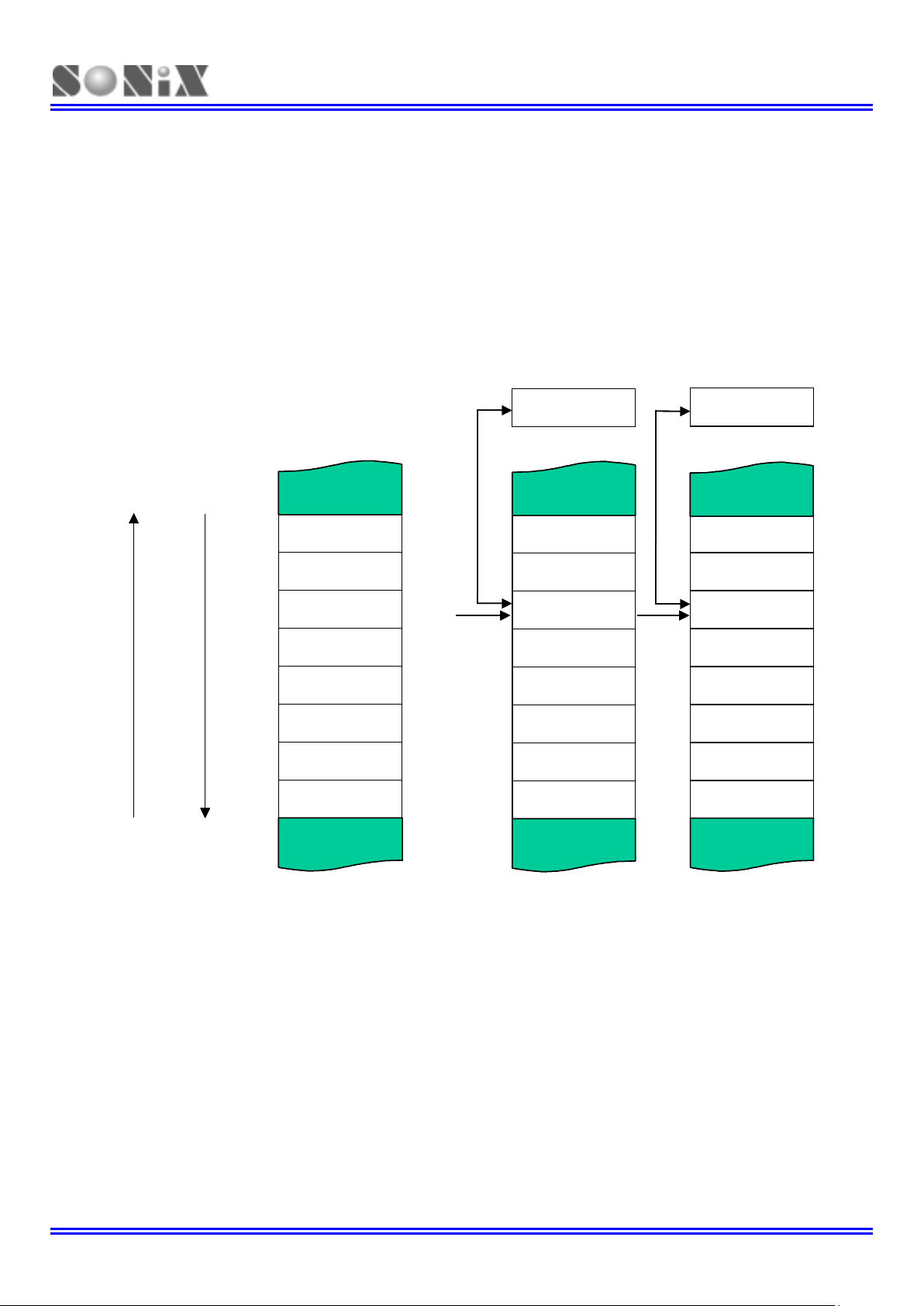
STACK OPERATIONS
OVERVIEW
The stack buffer of SN8P1702A/SN8P1703A has 8-level high area and each level is 12-bits length. This buffer is
designed to save and restore program counter’s (PC) data when interrupt service is executed. The STKP register is a
pointer designed to point active level in order to save or restore data from stack buffer for kernel circuit. The STKnH
and STKnL are the 12-bit stack buffers to store program counter (PC) data.
Figure 3-3 Stack-Save and Stack-Restore Operation
STACK BUFFER
STK7H
STK6H
STK5H
STK4H
STK3H
STK2H
STK1H
STK0H
STK7L
STK6L
STK5L
STK4L
STK3L
STK2L
STK1L
STK0L
STKP = 0
STKP = 1
STKP = 2
STKP = 3
STKP = 4
STKP = 5
STKP = 6
STKP = 7
STKP - 1
STKP + 1
CALL /
interrupt
RET /
RETI
STKP
PCH
PCL
STKP
STACK BUFFER
STK7H
STK6H
STK5H
STK4H
STK3H
STK2H
STK1H
STK0H
STK7L
STK6L
STK5L
STK4L
STK3L
STK2L
STK1L
STK0L
STK7H
STK6H
STK5H
STK4H
STK3H
STK2H
STK1H
STK0H
STK7L
STK6L
STK5L
STK4L
STK3L
STK2L
STK1L
STK0L
STKP = 0
STKP = 1
STKP = 2
STKP = 3
STKP = 4
STKP = 5
STKP = 6
STKP = 7
STKP = 0
STKP = 1
STKP = 2
STKP = 3
STKP = 4
STKP = 5
STKP = 6
STKP = 7
STKP - 1
STKP + 1
STKP - 1STKP - 1
STKP + 1
CALL /
interrupt
RET /
RETI
STKPSTKP
PCH
PCL
PCHPCH
PCLPCL
STKPSTKP
Preliminary SN8P1702A/SN8P1703A
8-bit micro-controller build-in 12-bit ADC
SONiX TECHNOLOGY CO., LTD Page 30 Revision 0.5
STACK REGISTERS
The stack pointer (STKP) is a 4-bit register to store the address used to access the stack buffer, 12-bits data memory
(STKnH and STKnL) set aside for temporary storage of stack addresses.
The two stack operations are writing to the top of the stack (Stack-Save) and reading (Stack-Restore) from the top of
stack. Stack-Save operation decrements the STKP and the Stack-Restore operation increments one time. That makes
the STKP always points to the top address of stack buffer and writes the last program counter value (PC) into the stack
buffer.
The program counter (PC) value is stored in the stack buffer before a CALL instruction executed or during interrupt
service routine. Stack operation is a LIFO type (Last in and first out). The stack pointer (STKP) and stack buffer
(STKnH and STKnL) are located in the system register area bank 0.
STKP (stack pointer) initial value = 0xxx 1111
0DFH Bit 7 Bit 6 Bit 5 Bit 4 Bit 3 Bit 2 Bit 1 Bit 0
STKP
GIE - - - STKPB3 STKPB2 STKPB1 STKPB0
R/W - - - R/W R/W R/W R/W
STKPBn: Stack pointer. (n = 0 ~ 3)
GIE: Global interrupt control bit. 0 = disable, 1 = enable. More detail information is in interrupt chapter.
Example: Stack pointer (STKP) reset routine.
MOV A, #00001111B
B0MOV STKP, A
STKn (stack buffer) initial value = xxxx xxxx xxxx xxxx, STKn = STKnH + STKnL (n = 7 ~ 0)
0F0H~0FFH Bit 7 Bit 6 Bit 5 Bit 4 Bit 3 Bit 2 Bit 1 Bit 0
STKnH
- - - - - - SnPC9 SnPC8
- - - - - - R/W R/W
0F0H~0FFH Bit 7 Bit 6 Bit 5 Bit 4 Bit 3 Bit 2 Bit 1 Bit 0
STKnL
SnPC7 SnPC6 SnPC5 SnPC4 SnPC3 SnPC2 SnPC1 SnPC0
R/W R/W R/W R/W R/W R/W R/W R/W
STKnH: Store PCH data as interrupt or call executing. The n expressed 0 ~7.
STKnL: Store PCL data as interrupt or call executing. The n expressed 0 ~7.
 Loading...