

SONIX SN8P0111P, SN8P0111S, SN8P0112P, SN8P0112S, SN8P0113P Datasheet
...
SN8P021X/8P011X
SN8P021X/8P011X 8-bit microcontroller
1. GENERAL DESCRIPTION
he SN8P021X/8P011X is an 8-bit micro-controller utilized with CMOS technology fabrication and featured with low power
T
consumption and high performance by its unique electronic structure. This chip is designed with the excellent IC structure,
including the program memory up to 2K/1K-word OTP ROM, 64 bytes of the data memory, one 8-bit T0 basic timer, one 8-bit
timer/event counter, a watch dog timer, three interrupt sources (T0, TC0, INT0), 13 I/O pins and 8 levels stack buffer. Besides,
the user can choose desired oscillator configurations for the controller. There are three oscillator configurations to select for
generating system clock, including high-performing crystal, ceramic resonator or cost-saving RC.
2. FEATURES
Memory configuration
♦
OTP ROM size : 2048 * 16 bits for SN8P021X series Two internal interrupts : T0, TC0
OTP ROM size : 1024 * 16 bits for SN8P011X series One external interrupt : INT0
RAM size : 64 * 8 bits.
I/O pin configuration
♦
One input port : 1 pin with wakeup function.
Two Input/output ports : 12 pins.
56 powerful instructions
♦♦♦♦
All of instructions are 1 word with 1 or 2 cycles'
execution.
Execution time : 1 cycle uses 4 clocks of oscillator.
All ROM area JMP instruction.
All ROM area Subroutine CALL instruction.
All ROM area lookup table function. (MOVC
instruction)
3. PIN ASSIGNMENT
(Total 13 pins)
Three interrupt sources :
♦
Eight levels stack buffer
♦
An 8-bit basic timer.
♦
An 8-bit timer/event counter.
♦
A watchdog timer.
♦
Acceptable oscillator type :
♦
Crystal or ceramic resonator up to 8MHz
RC oscillator up to 2 MHz
Package :
♦♦♦♦
PDIP : 16, 18, 20
SOP : 16, 18, 20
P1.2 1 U 20 P1.1
P1.2 1 U 18 P1.1 P1.3 2 19 P1.0
P1.1 1 U 16 P1.0 P1.3 2 17 P1.0 INT0/P0.0 3 18 XIN
INT0/P0.0 2 15 XIN INT0/P0.0 3 16 XIN VPP/RST 4 17 XOUT
VPP/RST 3 14 XOUT VPP/RST 4 15 XOUT VSS 5 16 VDD
VSS 4 13 VDD VSS 5 14 VDD VSS 6 15 VDD
P2.0 5 12 P2.7 P2.0 6 13 P2.7 P2.0 7 14 P2.7
P2.1 6 11 P2.6 P2.1 7 12 P2.6 P2.1 8 13 P2.6
P2.2 7 10 P2.5 P2.2 8 11 P2.5 P2.2 9 12 P2.5
P2.3 8 9 P2.4 P2.3 9 10 P2.4 P2.3 10 11 P2.4
SN8P0211P SN8P0212P SN8P0213P
SN8P0211S SN8P0212S SN8P0213S
SN8P0111P SN8P0112P SN8P0113P
SN8P0111S SN8P0112S SN8P0113S
SONiX TECHNOLOGY CO., LTD
Page 1
Preliminary
January 2000
SN8P021X/8P011X
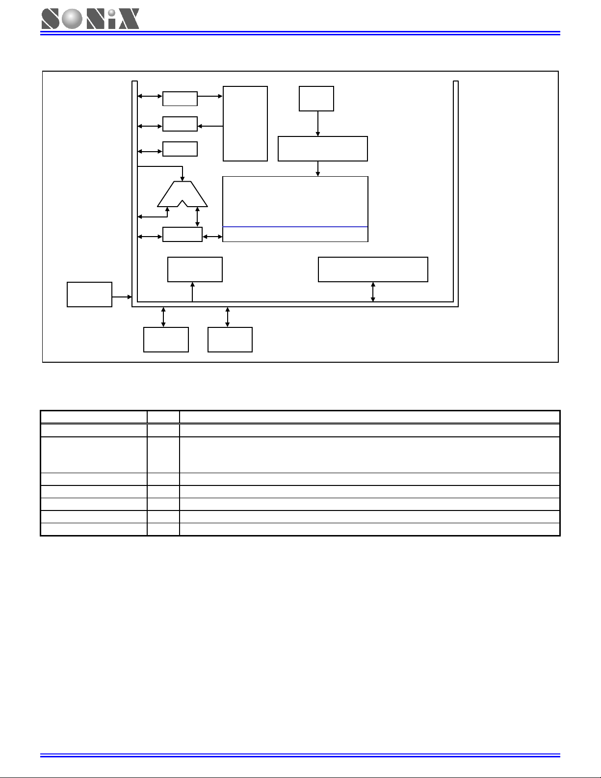
4. BLOCK DIAGRAM
PORT 0
PC
IR
FLAGS
ALU
ACC
INTERRUPT
CONTROL
H-OSC
OTP
ROM
TIMING GENERATOR
RAM
SYSTEM REGISTER
TIMER & COUNTER
PORT 2PORT 1
5. PIN DESCRIPTION
PIN NAME TYPE DESCRIPTION
P1.0 ~ P1.3 I/O Port 1.0 ~ Port 1.3 bi-direction pins.
RST/VPP I System reset inputs pin. Schmitt trigger structure, active “low”, normal stay to “high”.
During program op-code, this pin be pull to 12.5Vdc to reset internal address counter and to
write data into OTP-ROM.
VDD, VSS P Power supply input pins.
P2.0 ~ P2.7 I/O Port 2.0 ~ Port 2.7 bi-direction pins.
XIN I Oscillator input pin.
XOUT O Oscillator output pin.
P0.0 / INT0 I Port 0.0 and INT0 trigger pin with schmitt trigger structure.
Note : In order to reduce power consumption, the following procedure must be setup.
a). In the SN8P0211/8P0111 version, P1.2 ~ P1.3 must be programmed to input mode with pull up resistor.
SONiX TECHNOLOGY CO., LTD
Page 2
Preliminary
January 2000
 Loading...