

SONIX SN6B000 Datasheet
SN6B000
Hi-Density LCD Driver with 8-bit Controller
GENERAL DESCRIPTIONS
SN6B000 is a 8-bit micro controller series with hi-density LCD driver. Combined
with one or more SN6BS00 (64-segment drivers), SN6B000 can form one 1024/
2048/ 4096/ 6144/ 8192 dots LCD system. A dual-tone melody and a voice
synthesizer are included in SN6B000. Also, a 7-bit current-type DAC and the
PWM circuit are built in SN6B000, so that makes users easily choose a speaker
(DA), or a buzzer (PWM) for their applications. SN6B000 only contains 32 COM
signals of LCD. All segment signals are provided by SN6BS00. Several
different types of LCD applications can be implemented by suitably combining
SN6B000 and SN6BS00. SN6B000 not only contains internal mask ROM itself
(128K words, MC mode), but also possesses the interface to access external
ROM (maximum 512K words, MP mode). A memory chip, SN6B400 consists of
256K-word mask ROM and is available to work with SN6B000 to accomplish the
whole micro-processor system.
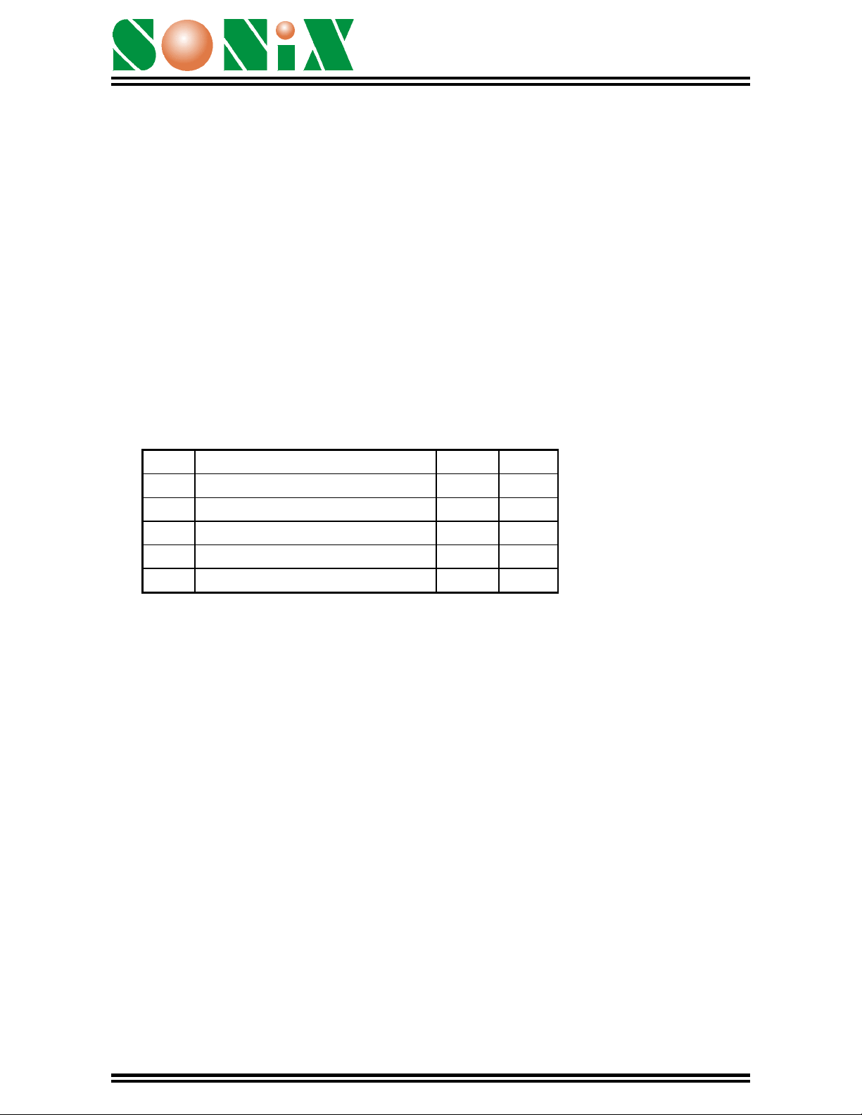
Dots Configuration COM SEG
1024
2048
4096
6144
8192
1 SN6B000 + l SN6BS00
1 SN6B000 + l SN6BS00
1 SN6B000 + 2 SN6BS00
1 SN6B000 + 3 SN6BS00
1 SN6B000 + 4 SN6BS00
16 64
32 64
32 128
32 192
32 256
1
December 20, 2000
Hi-Density LCD Driver with 8-bit Controller
FEATURES
ROM space: 512K words (=219*16=220*8); Program Space: 256K*16
MC mode:128K words in SN6B000
−
MP mode: along with SN6B400 to 256K words
−
RAM Size:
256 bytes in SN6B000
−
4*256 bytes in SN6BS00 (2*256 bytes LCD RAM, 2*256 bytes normal
−
RAM)
I/O Port : There are Port0 and Port1 (total 16 pins I/O)
All ports are I/O-type and P0.7 can be modulated with a carry signal
−
Each port can be set as “H”, ”L”,
−
(150K@5V
Every port can wake up chip when chip is in power-down mode
−
60 instructions
8 levels stack buffer supports interrupt and call subroutine
System Clock:
2MHz RC oscillator
−
2M/ 4M(3.58M) crystal
−
Low speed clock: Register option, 32768 crystal or RC
Three different operation modes can be selected:
Normal mode (both High/Low osc. On).
−
Slow mode (High osc. Off, Low osc. On).
−
Stop mode (both High and Low osc. Off).
−
LCD: 1/16 duty (for 1024) or 1/32 duty, frame rate=64 or 128 Hz.
A voltage regulator and double voltage circuit is included in SN6BS000
8 interrupt sources :
5 internal interrupts: T0, TC0, TC1, TW, SPEECH (non-maskable).
−
3 external interrupts: INTP0.0 ~ INTP0.2
−
ISR entry location: Reset: 0000, SPEECH: 0018h, and the others: 0008h
−
Voice:
Built-in voice synthesizer
−
Sampling rate from 4K to 40Khz
−
Dual tone melody with 4 octaves
−
7-bit DA converter (maximum 3mA)
−
PWM output for Buzzer
−
)
floating
, and
high-resistance “H”
SN6B000
2
December 20, 2000
Hi-Density LCD Driver with 8-bit Controller
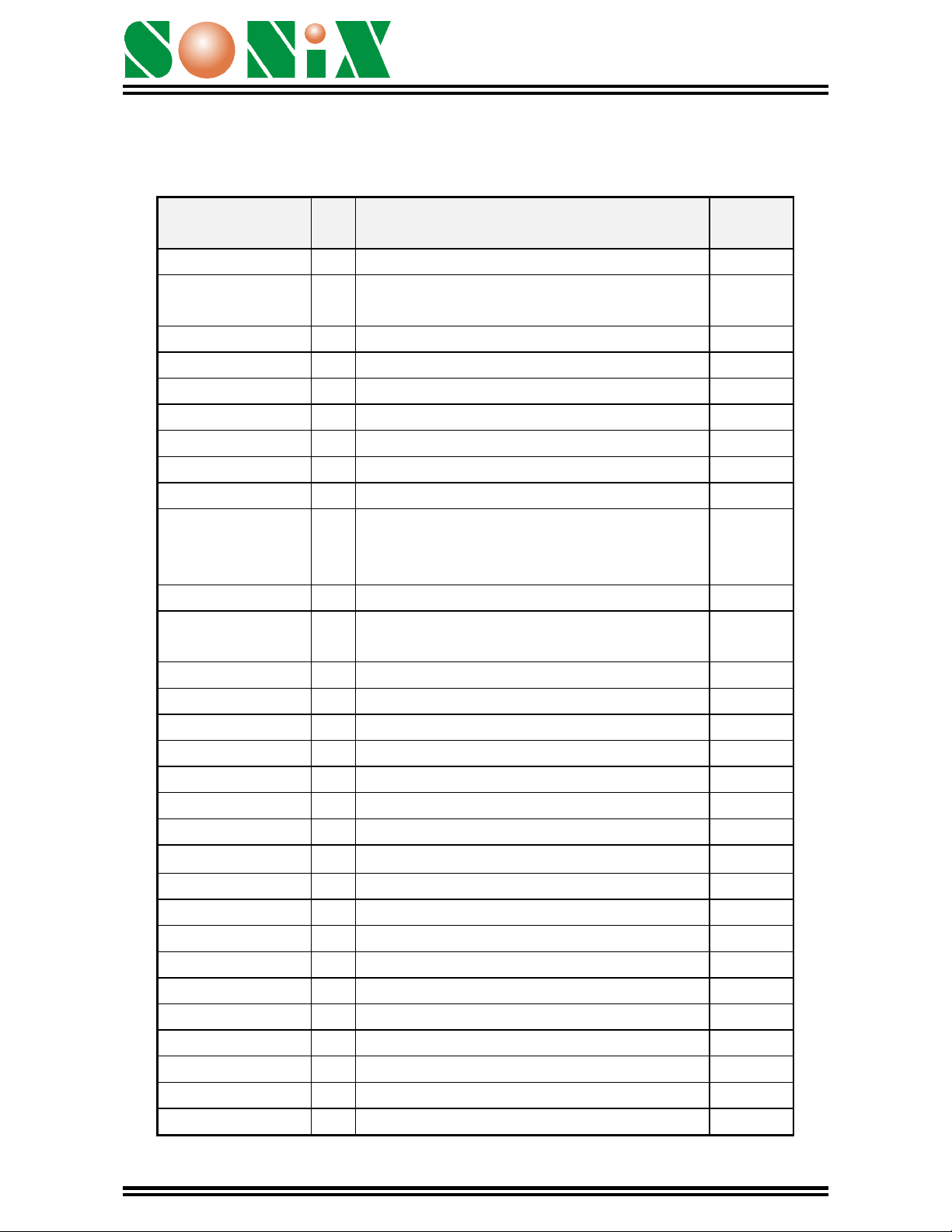
PIN ASSIGNMENT
SN6B000
Pin Name I/O Descriptions Internal
C0~C31 O Common 0 ~ 31
VLC1, VLC4,
VLC5
VLCDR I LCD Bias
P/C I Micro-processor/Micro-controller
A0~A19 O Address Bus for ROM
D0~D7 I/O Data Bus for ROM
CE1B O Chip Enable of External ROM.
VO/ BUZ1 O Voice out, 7-bit DA / PWM output
BUZ2 O PWM output
OSC/XIN High speed Clock input:
XOUT O High Speed clock output
CKSEL I High speed clock selection
LXIN I Low speed clock input
LXOUT O Low speed clock output
P0, P1 I/O I/O Ports
XCE_0 O Chip Enable of SN6BS00 0
XCE_1 O Chip Enable of SN6BS00 1
XCE_2 O Chip Enable of SN6BS00 2
XCE_3 O Chip Enable of SN6BS00 3
XD7~XD0 I/O Data Bus to Slave Driver
I LCD Bias
CKSEL=L, RC oscillator
CKSEL=H, Crystal
( 0:2M RC oscillator, 1: Crystal)
SN6B000
Pull-low
√
√
XA9~XA0 O Address Bus to Slave Driver
WR O Read Write signal
FRAME O Frame Synchronous Signal
CL O Display Synchronous Signal
M O Alternating signal for LCD
SYNC O Phase 1 synchronous pin.
TEST I Test Pin
RESETB I Reset Pin
VDD I Positive power supply
GND I Negative power supply
3
√
December 20, 2000
Hi-Density LCD Driver with 8-bit Controller
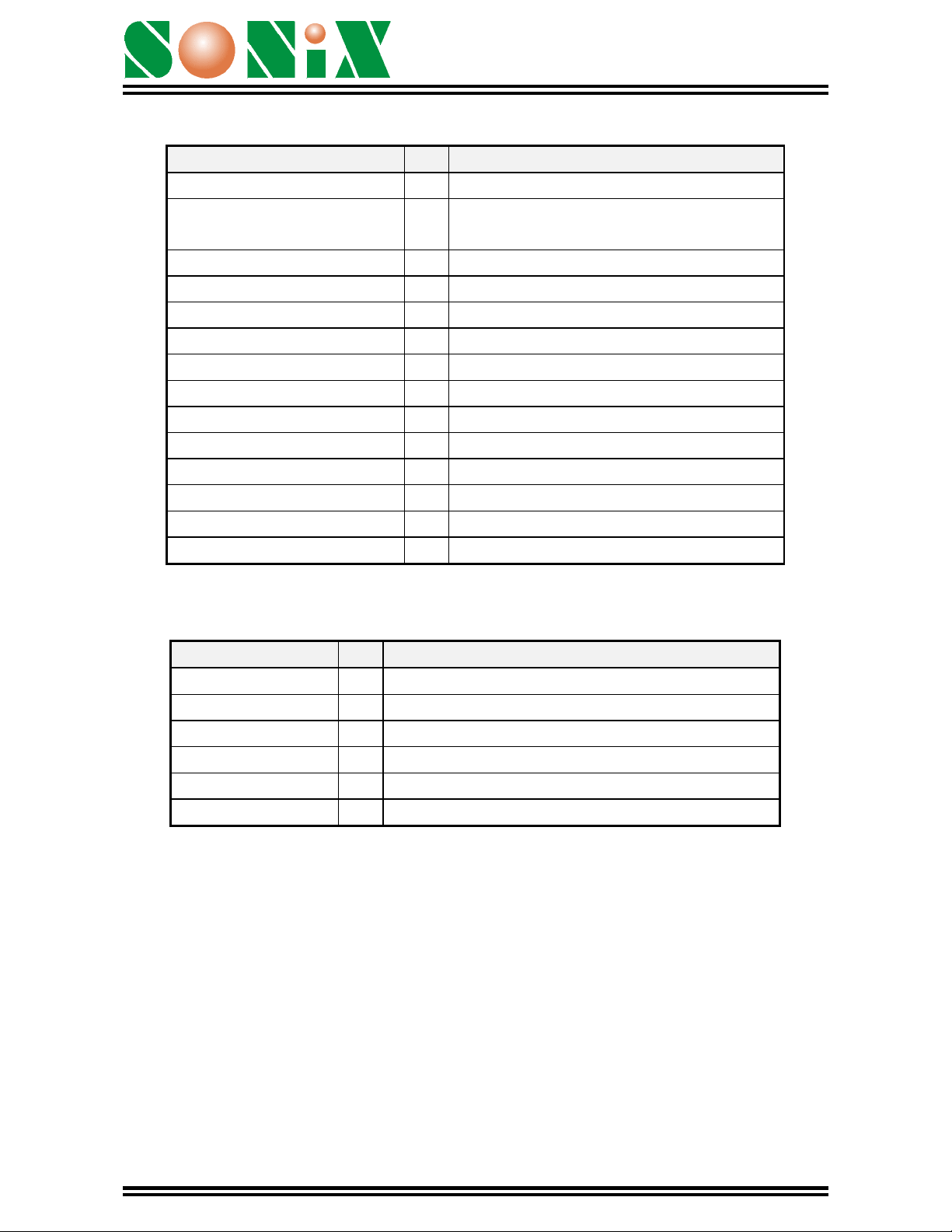
SN6BS00:
Pin Name I/O Descriptions
S0~S63 O Segment 0 ~ 63
VLCDR, VLC2, VLC3,
I LCD Bias
VLC5
VREG O Voltage Pumper
VPS I Voltage Pumper
VO1, VO2 I Voltage Pumper
XA0~XA9 I Address Bus
XD0~XD7 I/O Data Bus
XCE I Chip Enable
WR I Read Write signal
FRAME I Frame Synchronous Signal
CL I Display Synchronous Signal
M I Alternating signal for LCD
VDD I Positive power supply
GND I Negative power supply
SN6B000
SN6B400:
Pin Name I/O Function Description
V
DD
I Positive power supply
CEB I Chip Enable. (Active Low)
SYNC I Clock Pin
D7~D0 O Data Output
A18~A0 I Address Input
VSS I Negative power supply.
4
December 20, 2000
 Loading...