

SONIX SN65061 Datasheet

SN65061
Two Channels Direct Drive Speech Controller
INTRODUCTION
SN65061 is a 61 seconds two-channel single chip voice synthesizer IC which
contains a PWM Direct Drive Circuit and fixed current D/A output. There are two
4-bit I/O ports and built in a tiny controller. By programming through the tiny
controller, user’s applications including section combination, trigger modes,
output status, and other logic functions can be easily implemented.
FEATURES
Single power supply 2.4V – 5.1V
61 seconds voice capacity is provided
Built in a tiny controller
Two 4-bit I/O ports are provided
64*4 bits RAM are provided
Maximum 16k program ROM is provided
Readable ROM code data
Built in a high quality speech synthesizer
Adaptive playing speed from 2.5k-20kHz is provided
Two independent voice channels (Channel 1 + Channel 2→Buo1,Buo2)
Built in a PWM Direct Drive circuit and a fixed current D/A output
Low Voltage Reset
System clock : 2MHZ
1
December 20, 2000
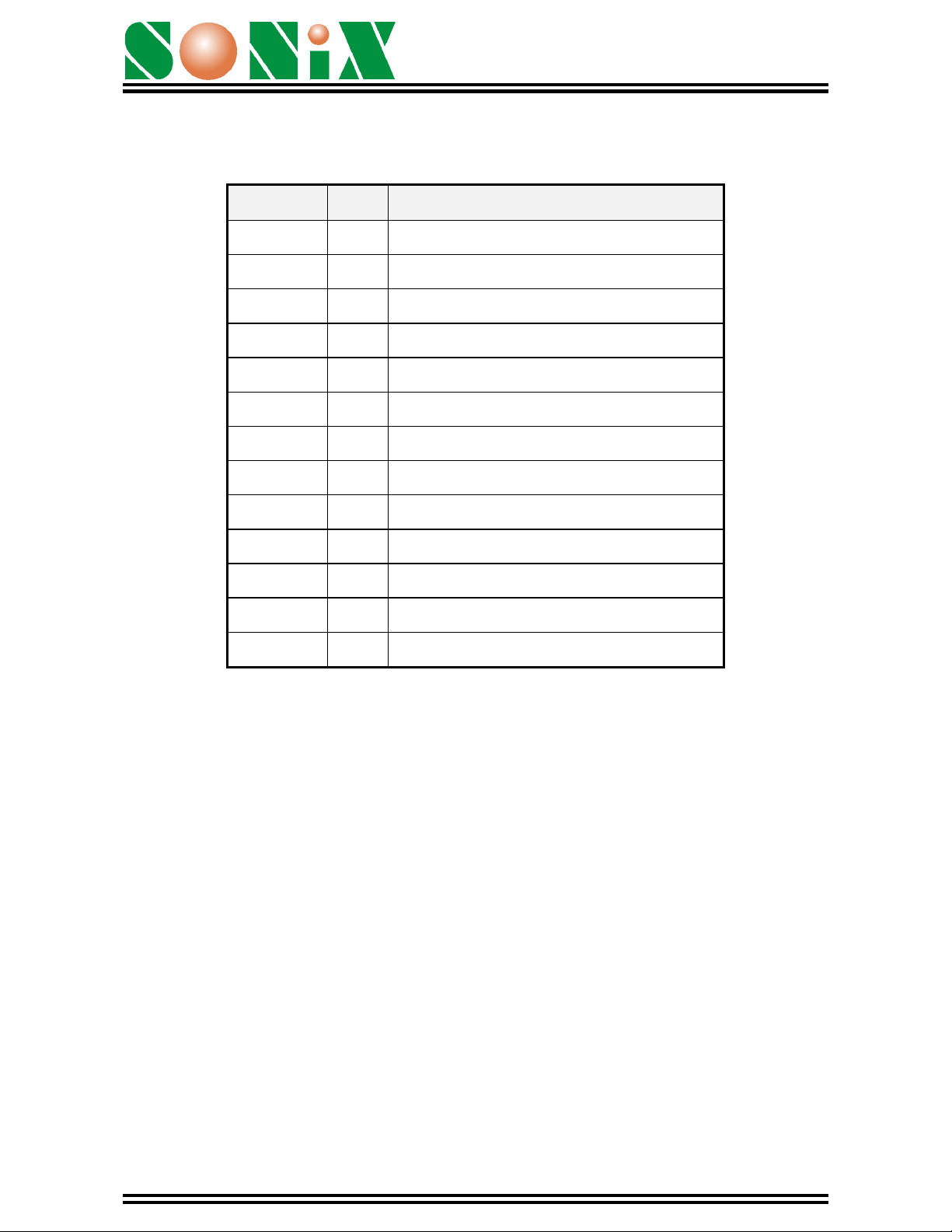
PIN ASSIGNMENT
Symbol I/O Function Description
P20 I/O Bit0 of I/O port 2
P21 I/O Bit1 of I/O port 2
P22 I/O Bit2 of I/O port 2
P23 I/O Bit3 of I/O port 2
P30 I/O Bit0 of I/O port 3
P31 I/O Bit1 of I/O port 3
P32 I/O Bit2 of I/O port 3
P33 I/O Bit3 of I/O port 3
SN65061
Two Channels Direct Drive Speech Controller
V
DD
I Positive power supply
OSC I Oscillation component connection pin
GND I Negative power supply
BUO1/VO O PWM output 1 / DA current output
BUO2 O PWM output 2
2
December 20, 2000
Two Channels Direct Drive Speech Controller
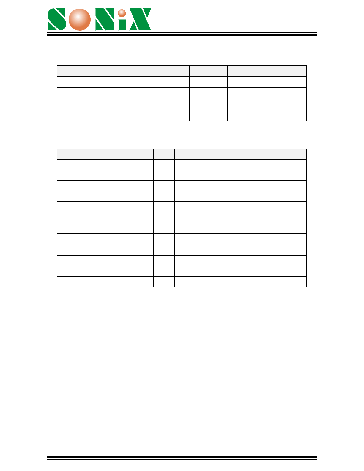
ABSOLUTE MAXIMUM RATINGS
Items Symbol Min Max Unit.
Supply Voltage VDD-V -0.3 6.0 V
SN65061
Input Voltage V
Operating Temperature T
Storage Temperature T
IN
OP
STG
ELECTRICAL CHARACTERISTICS
Item Sym. Min. Typ. Max. Unit Condition
Operating Voltage V
Standby current I
Operating Current I
SBY
OPR
Input current of P2, P3 I
Drive current of P2, P3 I
Sink Current of P2, P3 I
Drive current of Buo1 I
Sink Current of Buo1 I
Drive Current of Buo2 I
Sink Current of Buo2 I
OD
OS
OD
OS
OD
OS
Output current of VO Ivo 2.0 3.0 4.0
2.4 3.0 5.1 V
DD
--2.0uAVDD=3V, no load
- - 250
IH
- 3.0 10.0
1.5 2 -
2.0 3 -
100 120 -
100 120 -
100 120 -
100 120 -
GND-0.3 VDD+0.3 V
-20.0 70.0
-55.0 125.0
u
AVDD=3V, no load
u
AVDD=3V,VIN=3V
m
AVDD=3V,VO=2.4V
m
AVDD=3V,VO=0.4V
m
A VDD=3V,Buo1=1.5V
m
A VDD=3V,Buo1=1.5V
m
A VDD=3V,Buo2=1.5V
m
A VDD=3V,Buo2=1.5V
m
A VDD=3V,VO=0.7V
o
o
C
C
Oscillation Freq. F
OSC
-1.0-MHzVDD=3V
3
December 20, 2000
 Loading...