

Page 1

SN32F100 Series
SSO
ONNiiXX 3322--BBiitt CCoorrtteexx--
M
M00
M
Miiccrroo--CCoonnttrroolllleerr
32-Bit Cortex-M0 Micro-Controller
SN32F100 Series
USER’S MANUAL
SN32F107
SN32F108
SN32F109
SONIX reserves the right to make change without further notice to any products herein to improve reliability, function or design. SONIX does not
assume any liability arising out of the application or use of any product or circuit described herein; neither does it convey any license under its patent
rights nor the rights of others. SONIX products are not designed, intended, or authorized for us as components in systems intended, for surgical
implant into the body, or other applications intended to support or sustain life, or for any other application in which the failure of the SONIX product
could create a situation where personal injury or death may occur. Should Buyer purchase or use SONIX products for any such unintended or
unauthorized application. Buyer shall indemnify and hold SONIX and its officers, employees, subsidiaries, affiliates and distributors harmless against
all claims, cost, damages, and expenses, and reasonable attorney fees arising out of, directly or indirectly, any claim of personal injury or death
associated with such unintended or unauthorized use even if such claim alleges that SONIX was negligent regarding the design or manufacture of
the part.
SONiX TECHNOLOGY CO., LTD Page 1 Version 1.9
Page 2
SN32F100 Series
Version
Date
Description
1.0
2013/03/18
First version released.
1.1
2013/03/29
1. Update Codec Spec.
2. Update DAC Setting 3 Register.
3. Update Sigma-delta DAC Power-Up Sequence.
1.2
2013/04/02
1. Update Codec Spec.
2. Update ADC Setting 23 Register.
3. Update DAC Setting 1 Register and DAC Setting 2 Register.
1.3
2013/06/04
1. Add SN32F100 Start Kit V1.1 description.
2. Add Comparator Output Debounce Time.
3. Update supply current.
4. Add Operation Mode Comparison Table.
5. Update System Block Diagram.
6. Update System Tick Timer description.
7. Update LQFP 64 Pin Package Information.
8. Update Comparator description.
9. Modify ADC’s SEL_MIC definition.
1.4
2013/07/16
1. Update I2S’s Status register default value.
2. Update ADC’s SEL_MIC register default value.
3. Update Code Security diagram.
4. Update Code Option Table.
5. Update High-level and Low-level input voltage Spec.
6. Update P0.14/DPDWAKEUP pin description.
1.5
2014/02/27
1. Update Electrical characteristics.
2. Update Code Security table in Code Security section.
3. Add Note for I/O open-drain function.
4. Add descriptions of I2C events which trigger I2C interrupt for I2Cn_STAT register.
5. Update SN-LINK description in Chap 17. Development Tool.
6. Add Notice for BOOT pin in Chap 16. SWD.
7. Add WAKEUP sections.
8. Fix typing error.
1.6
2014/06/04
1. Update SN-LINK-V2 photos.
2. Fix typing errors.
1.7
2015/05/29
1. Update UART baud rate sample.
1.8
2016/07/22
1. Fix typing errors.
2. Add Notice: HCLK MUST be equal or less than 24MHz during Flash program and erase
operations.
3. Add SSPn Data Fetch (SSPn_DF) register.
4. Update LQFP48 package information.
1.9
2018/02/02
1. Fix typing errors.
2. Remove SYSTICKPRE[1:0]
3. Remove SYS0_ANTIEFT register.
4. Update WDTPRE[2:0] bits description in SYS1_APBCP1 register.
5. Update TO[15:0] bits description in I2Cn_TOCTRL register.
6. Add Note for setting the pins which are not pin-out.
32-Bit Cortex-M0 Micro-Controller
AMENDENT HISTORY
SONiX TECHNOLOGY CO., LTD Page 2 Version 1.9
Page 3

SN32F100 Series
1
1
1
2
2
2
3
3
3
32-Bit Cortex-M0 Micro-Controller
Table of Content
AMENDENT HISTORY ................................................................................................................................ 2
PRODUCT OVERVIEW ....................................................................................................................... 13
1.1 FEATURES ...................................................................................................................................... 13
1.2 SYSTEM BLOCK DIAGRAM ........................................................................................................ 15
1.3 CLOCK GENERATION BLOCK DIAGRAM ................................................................................ 16
1.4 PIN ASSIGNMENT ......................................................................................................................... 17
1.5 PIN DESCRIPTIONS ....................................................................................................................... 20
1.6 PIN CIRCUIT DIAGRAMS ............................................................................................................. 25
CENTRAL PROCESSOR UNIT (CPU) .............................................................................................. 27
2.1 MEMORY MAP ............................................................................................................................... 27
2.2 SYSTEM TICK TIMER ................................................................................................................... 28
2.2.1 OPERATION ............................................................................................................................ 28
2.2.2 SYSTICK USAGE HINTS AND TIPS ....................................................................................... 29
2.2.3 SYSTICK REGISTERS .............................................................................................................. 29
2.2.3.1 System Tick Timer Control and Status register (SYSTICK_CTRL) ................................... 29
2.2.3.2 System Tick Timer Reload value register (SYSTICK_LOAD) ........................................... 29
2.2.3.3 System Tick Timer Current Value register (SYSTICK_VAL) ............................................ 30
2.2.3.4 System Tick Timer Calibration Value register (SYST_CALIB) ......................................... 30
2.3 NESTED VECTORED INTERRUPT CONTROLLER (NVIC) ..................................................... 31
2.3.1 INTERRUPT AND EXCEPTION VECTORS ........................................................................... 31
2.3.2 NVIC REGISTERS .................................................................................................................... 31
2.3.2.1 IRQ0~31 Interrupt Set-Enable Register (NVIC_ISER) ....................................................... 32
2.3.2.2 IRQ0~31 Interrupt Clear-Enable Register (NVIC_ICER) ................................................... 32
2.3.2.3 IRQ0~31 Interrupt Set-Pending Register (NVIC_ISPR) ..................................................... 32
2.3.2.4 IRQ0~31 Interrupt Clear-Pending Register (NVIC_ICPR) ................................................. 32
2.3.2.5 IRQ0~31 Interrupt Priority Register (NVIC_IPRn) (n=0~7) ............................................... 33
2.4 APPLICATION INTERRUPT AND RESET CONTROL (AIRC) .................................................. 33
2.5 CODE OPTION TABLE .................................................................................................................. 35
2.6 CORE REGISTER OVERVIEW ..................................................................................................... 36
SYSTEM CONTROL............................................................................................................................. 37
3.1 RESET .............................................................................................................................................. 37
3.1.1 POWER-ON RESET (POR) ...................................................................................................... 37
3.1.2 WATCHDOG RESET (WDT RESET) ....................................................................................... 38
3.1.3 BROWN-OUT RESET............................................................................................................... 38
SONiX TECHNOLOGY CO., LTD Page 3 Version 1.9
Page 4

SN32F100 Series
32-Bit Cortex-M0 Micro-Controller
3.1.3.1 BROWN OUT DESCRIPTION ........................................................................................... 38
3.1.3.2 THE SYSTEM OPERATING VOLTAGE DECSRIPTION ............................................... 39
3.1.3.3 BROWN-OUT RESET IMPROVEMENT .......................................................................... 39
3.1.4 EXTERNAL RESET .................................................................................................................. 40
3.1.4.1 SIMPLY RC RESET CIRCUIT ........................................................................................... 41
3.1.4.2 DIODE & RC RESET CIRCUIT ......................................................................................... 41
3.1.4.3 ZENER DIODE RESET CIRCUIT ...................................................................................... 42
3.1.4.4 VOLTAGE BIAS RESET CIRCUIT ................................................................................... 42
3.1.4.5 EXTERNAL RESET IC ....................................................................................................... 43
3.1.5 SOFTWARE RESET ................................................................................................................. 43
3.2 SYSTEM CLOCK ............................................................................................................................ 44
3.2.1 INTERNAL RC CLOCK SOURCE ........................................................................................... 44
3.2.1.1 Internal High-speed RC Oscillator (IHRC) .......................................................................... 44
3.2.1.2 Internal Low-speed RC Oscillator (ILRC) ........................................................................... 44
3.2.2 PLL ........................................................................................................................................... 45
3.2.2.1 PLL Frequency selection ...................................................................................................... 45
3.2.3 EXTERNAL CLOCK SOURCE ................................................................................................ 46
3.2.3.1 External High-speed (EHS) Clock ....................................................................................... 46
3.2.3.2 CRYSTAL/CERAMIC ......................................................................................................... 46
3.2.3.3 Audio External High-speed (AUEHS) Clock ....................................................................... 47
3.2.3.4 External Low-speed (ELS) Clock......................................................................................... 47
3.2.3.5 CRYSTAL ............................................................................................................................ 47
3.2.3.6 Bypass Mode ........................................................................................................................ 48
3.2.4 SYSTEM CLOCK (SYSCLK) SELECTION............................................................................... 49
3.2.5 CLOCK-OUT CAPABITITY ..................................................................................................... 49
3.3 SYSTEM CONTROL REGISTERS 0 .............................................................................................. 50
3.3.1 Analog Block Control register (SYS0_ANBCTRL) ................................................................... 50
3.3.2 PLL control register (SYS0_PLLCTRL) ................................................................................... 50
3.3.2.1 RECOMMEND FREQUENCY SETTING.......................................................................... 51
3.3.3 Clock Source Status register (SYS0_CSST) .............................................................................. 52
3.3.4 System Clock Configuration register (SYS0_CLKCFG) .......................................................... 52
3.3.5 AHB Clock Prescale register (SYS0_AHBCP) ......................................................................... 52
3.3.6 System Reset Status register (SYS0_RSTST) ............................................................................ 53
3.3.7 LVD Control register (SYS0_LVDCTRL) ................................................................................. 53
3.3.8 External RESET Pin Control register (SYS0_EXRSTCTRL) ................................................... 55
3.3.9 SWD Pin Control register (SYS0_SWDCTRL) ......................................................................... 55
3.4 SYSTEM CONTROL REGISTERS 1 .............................................................................................. 56
3.4.1 AHB Clock Enable register (SYS1_AHBCLKEN) .................................................................... 56
3.4.2 APB Clock Prescale register 0 (SYS1_APBCP0) ..................................................................... 57
3.4.3 APB Clock Prescale register 1 (SYS1_APBCP1) ..................................................................... 58
SONiX TECHNOLOGY CO., LTD Page 4 Version 1.9
Page 5

SN32F100 Series
4
4
4
5
5
5
6
6
6
32-Bit Cortex-M0 Micro-Controller
3.4.4 Peripheral Reset register (SYS1_PRST) ................................................................................... 59
SYSTEM OPERATION MODE ........................................................................................................... 61
4.1 OVERVIEW ..................................................................................................................................... 61
4.2 NORMAL MODE ............................................................................................................................ 61
4.3 LOW-POWER MODES ................................................................................................................... 61
4.3.1 SLEEP MODE .......................................................................................................................... 61
4.3.2 DEEP-SLEEP MODE............................................................................................................... 62
4.3.3 DEEP POWER-DOWN (DPD) MODE .................................................................................... 62
4.3.3.1 Entering Deep power-down mode ........................................................................................ 63
4.3.3.2 Exiting Deep power-down mode .......................................................................................... 63
4.4 WAKEUP INTERRUPT .................................................................................................................. 63
4.5 WAKEUP ......................................................................................................................................... 63
4.5.1 OVERVIEW .............................................................................................................................. 63
4.5.2 WAKEUP TIME ........................................................................................................................ 63
4.6 STATE MACHINE OF PMU ........................................................................................................... 64
4.7 OPERATION MODE COMPARSION TABLE .............................................................................. 65
4.8 PMU REGISTERS ........................................................................................................................... 66
4.8.1 Backup registers 0 to 15 (PMU_BKP0~15) ............................................................................. 66
4.8.2 Power control register (PMU_CTRL) ...................................................................................... 66
GENERAL PURPOSE I/O PORT (GPIO) .......................................................................................... 67
5.1 OVERVIEW ..................................................................................................................................... 67
5.2 GPIO MODE .................................................................................................................................... 67
5.3 GPIO REGISTERS ........................................................................................................................... 68
5.3.1 GPIO Port n Data register (GPIOn_DATA) (n=0,1,2,3)......................................................... 68
5.3.2 GPIO Port n Mode register (GPIOn_MODE) (n=0,1,2,3) ...................................................... 68
5.3.3 GPIO Port n Configuration register (GPIOn_CFG) (n=0,1,2,3) ............................................ 68
5.3.4 GPIO Port n Interrupt Sense register (GPIOn_IS) (n=0,1,2,3) ............................................... 70
5.3.5 GPIO Port n Interrupt Both-edge Sense register (GPIOn_IBS) (n=0,1,2,3) ........................... 70
5.3.6 GPIO Port n Interrupt Event register (GPIOn_IEV) (n=0,1,2,3) ............................................ 70
5.3.7 GPIO Port n Interrupt Enable register (GPIOn_IE) (n=0,1,2,3) ............................................ 70
5.3.8 GPIO Port n Raw Interrupt Status register (GPIOn_RIS) (n=0,1,2,3) ................................... 71
5.3.9 GPIO Port n Interrupt Clear register (GPIOn_IC) (n=0,1,2,3) .............................................. 71
5.3.10 GPIO Port n Bits Set Operation register (GPIOn_BSET) (n=0,1,2,3) .................................... 71
5.3.11 GPIO Port n Bits Clear Operation register (GPIOn_BCLR) (n=0,1,2,3) ............................... 71
5.3.12 GPIO Port n Open-Drain Control register (GPIOn_ODCTRL) (n=0,1,2,3) .......................... 71
16-BIT TIMER WITH CAPTURE FUNCTION ................................................................................ 74
6.1 OVERVIEW ..................................................................................................................................... 74
6.2 FEATURES ...................................................................................................................................... 74
SONiX TECHNOLOGY CO., LTD Page 5 Version 1.9
Page 6

SN32F100 Series
7
7
7
32-Bit Cortex-M0 Micro-Controller
6.3 PIN DESCRIPTION ......................................................................................................................... 74
6.4 BLOCK DIAGRAM ......................................................................................................................... 75
6.5 TIMER OPERATION ...................................................................................................................... 76
6.6 PWM ................................................................................................................................................. 77
6.7 CT16BN REGISTERS ...................................................................................................................... 78
6.7.1 CT16Bn Timer Control register (CT16Bn_TMRCTRL) (n=0,1) ............................................. 78
6.7.2 CT16Bn Timer Counter register (CT16Bn_TC) (n=0,1) ......................................................... 78
6.7.3 CT16Bn Prescale register (CT16Bn_PRE) (n=0,1) ................................................................. 78
6.7.4 CT16Bn Prescale Counter register (CT16Bn_PC) (n=0,1) ..................................................... 78
6.7.5 CT16Bn Count Control register (CT16Bn_CNTCTRL) (n=0,1) .............................................. 79
6.7.6 CT16Bn Match Control register (CT16Bn_MCTRL) (n=0,1) ................................................. 79
6.7.7 CT16Bn Match register 0~3 (CT16Bn_MR0~3) (n=0,1) ......................................................... 80
6.7.8 CT16Bn Capture Control register (CT16Bn_CAPCTRL) (n=0,1) .......................................... 80
6.7.9 CT16Bn Capture 0 register (CT16Bn_CAP0) (n=0,1) ............................................................ 81
6.7.10 CT16Bn External Match register (CT16Bn_EM) (n=0,1) .................................................... 81
6.7.11 CT16Bn PWM Control register (CT16Bn_PWMCTRL) (n=0,1) ............................................. 81
6.7.12 CT16Bn Timer Raw Interrupt Status register (CT16Bn_RIS) (n=0,1) .................................... 82
6.7.13 CT16Bn Timer Interrupt Clear register (CT16Bn_IC) (n=0,1) ............................................... 82
32-BIT TIMER WITH CAPTURE FUNCTION ................................................................................ 83
7.1 OVERVIEW ..................................................................................................................................... 83
7.2 FEATURES ...................................................................................................................................... 83
7.3 PIN DESCRIPTION ......................................................................................................................... 83
7.4 BLOCK DIAGRAM ......................................................................................................................... 84
7.5 TIMER OPERATION ...................................................................................................................... 85
7.6 PWM ................................................................................................................................................. 86
7.7 CT32BN REGISTERS ...................................................................................................................... 87
7.7.1 CT32Bn Timer Control register (CT32Bn_TMRCTRL) (n=0,1) ............................................. 87
7.7.2 CT32Bn Timer Counter register (CT32Bn_TC) (n=0,1) ......................................................... 87
7.7.3 CT32Bn Prescale register (CT32Bn_PRE) (n=0,1) ................................................................. 87
7.7.4 CT32Bn Prescale Counter register (CT32Bn_PC) (n=0,1) ..................................................... 87
7.7.5 CT32Bn Count Control register (CT32Bn_CNTCTRL) (n=0,1) .............................................. 88
7.7.6 CT32Bn Match Control register (CT32Bn_MCTRL) (n=0,1) ................................................. 88
7.7.7 CT32Bn Match register 0~3 (CT32Bn_MR0~3) (n=0,1) ......................................................... 89
7.7.8 CT32Bn Capture Control register (CT32Bn_CAPCTRL) (n=0,1) .......................................... 89
7.7.9 CT32Bn Capture 0 register (CT32Bn_CAP0) (n=0,1) ............................................................ 90
7.7.10 CT32Bn External Match register (CT32Bn_EM) (n=0,1) ....................................................... 90
7.7.11 CT32Bn PWM Control register (CT32Bn_PWMCTRL) (n=0,1) ............................................. 90
7.7.12 CT32Bn Timer Raw Interrupt Status register (CT32Bn_RIS) (n=0,1) .................................... 91
7.7.13 CT32Bn Timer Interrupt Clear register (CT32Bn_IC) (n=0,1) ............................................... 91
SONiX TECHNOLOGY CO., LTD Page 6 Version 1.9
Page 7

SN32F100 Series
8
8
8
9
9
9
1
1
1
0
0
0
32-Bit Cortex-M0 Micro-Controller
WATCHDOG TIMER (WDT) .............................................................................................................. 92
8.1 OVERVIEW ..................................................................................................................................... 92
8.2 BLOCK DIAGRAM ......................................................................................................................... 93
8.3 WDT REGISTERS ........................................................................................................................... 94
8.3.1 Watchdog Configuration register (WDT_CFG) ....................................................................... 94
8.3.2 Watchdog Clock Source register (WDT_CLKSOURCE) ......................................................... 94
8.3.3 Watchdog Timer Constant register (WDT_TC)........................................................................ 94
8.3.4 Watchdog Feed register (WDT_FEED) ................................................................................... 95
REAL-TIME CLOCK (RTC) ............................................................................................................... 96
9.1 OVERVIEW ..................................................................................................................................... 96
9.2 FEATURES ...................................................................................................................................... 96
9.3 FUNCTIONAL DESCRIPTION ...................................................................................................... 96
9.3.1 INTRODUCTION ..................................................................................................................... 96
9.3.2 RESET RTC REGISTERS ......................................................................................................... 96
9.3.3 RTC FLAG ASSERTION .......................................................................................................... 96
9.3.4 RTC OPERATION .................................................................................................................... 97
9.4 BLOCK DIAGRAM ......................................................................................................................... 98
9.5 RTC REGISTERS ............................................................................................................................ 99
9.5.1 RTC Control register (RTC_CTRL) ......................................................................................... 99
9.5.2 RTC Clock Source Select register (RTC_CLKS) ...................................................................... 99
9.5.3 RTC Interrupt Enable register (RTC_IE) ................................................................................. 99
9.5.4 RTC Raw Interrupt Status register (RTC_RIS) ........................................................................ 99
9.5.5 RTC Interrupt Clear register (RTC_IC) ................................................................................. 100
9.5.6 RTC Second Counter Reload Value register (RTC_SECCNTV) ............................................ 100
9.5.7 RTC Second Count register (RTC_SECCNT) ........................................................................ 100
9.5.8 RTC Alarm Counter Reload Value register (RTC_ALMCNTV) ............................................. 100
9.5.9 RTC Alarm Count register (RTC_ALMCNT) ......................................................................... 101
SPI/SSP .............................................................................................................................................. 102
10.1 OVERVIEW ................................................................................................................................... 102
10.2 FEATURES .................................................................................................................................... 102
10.3 PIN DESCRIPTION ....................................................................................................................... 103
10.4 INTERFACE DESCRIPTION ....................................................................................................... 104
10.4.1 SPI .......................................................................................................................................... 104
10.4.2 SSI ........................................................................................................................................... 105
10.4.3 COMMUNICATION FLOW ................................................................................................... 105
10.4.3.1 SINGLE-FRAME ........................................................................................................... 105
10.4.3.2 MULTI-FRAME ............................................................................................................ 106
10.5 AUTO-SEL (AUTO-CS) ................................................................................................................... 106
SONiX TECHNOLOGY CO., LTD Page 7 Version 1.9
Page 8

SN32F100 Series
1
1
1
1
1
1
1
1
1
2
2
2
32-Bit Cortex-M0 Micro-Controller
10.6 SSP REGISTERS ........................................................................................................................... 107
10.6.1 SSP n Control register 0 (SSPn_CTRL0) (n=0, 1) ................................................................. 107
10.6.2 SSP n Control register 1 (SSPn_CTRL1) (n=0, 1) ................................................................. 108
10.6.3 SSP n Clock Divider register (SSPn_CLKDIV) (n=0, 1) ....................................................... 108
10.6.4 SSP n Status register (SSPn_STAT) (n=0, 1) ......................................................................... 108
10.6.5 SSP n Interrupt Enable register (SSPn_IE) (n=0, 1) ............................................................. 109
10.6.6 SSP n Raw Interrupt Status register (SSPn_RIS) (n=0, 1) ..................................................... 109
10.6.7 SSP n Interrupt Clear register (SSPn_IC) (n=0, 1) ............................................................... 109
10.6.8 SSP n Data register (SSPn_DATA) (n=0, 1) .......................................................................... 110
10.6.9 SSP n Data Fetch register (SSPn_DF) (n=0, 1) .................................................................... 110
I2C ...................................................................................................................................................... 111
11.1 OVERVIEW ................................................................................................................................... 111
11.2 FEATURES .................................................................................................................................... 111
11.3 PIN DESCRIPTION ....................................................................................................................... 112
11.4 WAVE CHARACTERISTICS ....................................................................................................... 112
11.5 I2C MASTER MODES .................................................................................................................. 113
11.5.1 MASTER TRANSMITTER MODE .......................................................................................... 113
11.5.2 MASTER RECEIVER MODE ................................................................................................. 113
11.5.3 ARBITRATION ....................................................................................................................... 113
11.6 I2C SLAVE MODES ...................................................................................................................... 114
11.6.1 SLAVE TRANSMITTER MODE ............................................................................................. 114
11.6.2 SLAVE RECEIVER MODE .................................................................................................... 114
11.7 MONITOR MODE ......................................................................................................................... 115
11.7.1 INTERRUPT ........................................................................................................................... 115
11.7.2 LOSS of ARBITRATION ......................................................................................................... 115
11.8 I2C REGISTERS ............................................................................................................................ 116
11.8.1 I2C n Control register (I2Cn_CTRL) (n=0,1) ........................................................................ 116
11.8.2 I2C n Status register (I2Cn_STAT) (n=0,1) ........................................................................... 117
11.8.3 I2C n TX Data register (I2Cn_TXDATA) (n=0,1) ................................................................. 118
11.8.4 I2C n RX Data register (I2Cn_RXDATA) (n=0,1) ................................................................. 118
11.8.5 I2C n Slave Address 0 register (I2Cn_SLVADDR0) (n=0,1) ................................................. 118
11.8.6 I2C n Slave Address 1~3 register (I2Cn_SLVADDR1~3) (n=0,1) ........................................ 118
11.8.7 I2C n SCL High Time register (I2Cn_SCLHT) (n=0,1) ......................................................... 118
11.8.8 I2C n SCL Low Time register (I2Cn_SCLLT) (n=0,1) ........................................................... 119
11.8.9 I2C n Timeout Control register (I2Cn_TOCTRL) (n=0,1) .................................................... 119
11.8.10 I2C n Monitor Mode Control register (I2Cn_MMCTRL) (n=0,1) ..................................... 119
UNIVERSAL ASYNCHRONOUS RECEIVER AND TRANSMITTER (UART) .................... 121
12.1 OVERVIEW ................................................................................................................................... 121
SONiX TECHNOLOGY CO., LTD Page 8 Version 1.9
Page 9

SN32F100 Series
1
1
1
3
3
3
32-Bit Cortex-M0 Micro-Controller
12.2 FEATURES .................................................................................................................................... 121
12.3 PIN DESCRIPTION ....................................................................................................................... 121
12.4 BLOCK DIAGRAM ....................................................................................................................... 122
12.5 BAUD RATE CALCULATION .................................................................................................... 123
12.6 AUTO-BAUD FLOW .................................................................................................................... 124
12.6.1 AUTO-BAUD .......................................................................................................................... 124
12.6.2 AUTO-BAUD MODES ........................................................................................................... 125
12.7 UART REGISTERS ....................................................................................................................... 127
12.7.1 UART n Receiver Buffer register (UARTn_RB) (n=0, 1) ....................................................... 127
12.7.2 UART n Transmitter Holding register (UARTn_TH) (n=0, 1) ............................................... 127
12.7.3 UART n Divisor Latch LSB registers (UARTn_DLL) (n =0, 1) ............................................. 127
12.7.4 UART n Divisor Latch MSB register (UARTn_DLM) (n=0,1) .............................................. 127
12.7.5 UART n Interrupt Enable register (UARTn_IE) (n=0, 1) ...................................................... 128
12.7.6 UART n Interrupt Identification register (UARTn_II) (n=0,1) .............................................. 128
12.7.7 UART n FIFO Control register (UARTn_FIFOCTRL) (n=0,1)............................................. 130
12.7.8 UART n Line Control register (UARTn_LC) (n=0,1) ............................................................ 130
12.7.9 UART n Line Status register (UARTn_LS) (n=0,1) ................................................................ 130
12.7.10 UART n Scratch Pad register (UARTn_SP) (n=0, 1) ......................................................... 132
12.7.11 UART n Auto-baud Control register (UARTn_ABCTRL) (n=0, 1) .................................... 132
12.7.12 UART n Fractional Divider register (UARTn_FD) (n=0, 1) ............................................. 132
12.7.13 UART n Control register (UARTn_CTRL) (n=0, 1) ........................................................... 133
12.7.14 UART n Half-duplex Enable register (UARTn_HDEN) (n=0, 1) ...................................... 133
AUDIO (I2S/CODEC) ...................................................................................................................... 135
13.1 OVERVIEW ................................................................................................................................... 135
13.1.1 I2S Description ....................................................................................................................... 135
13.1.2 Codec Description .................................................................................................................. 135
13.2 FEATURES .................................................................................................................................... 135
13.2.1 I2S Features ............................................................................................................................ 135
13.2.2 Codec Features ....................................................................................................................... 135
13.3 PIN DESCRIPTION ....................................................................................................................... 136
13.3.1 I2S Pin Description ................................................................................................................ 136
13.3.2 Codec Pin Description............................................................................................................ 136
13.3.3 Audio Clock Pin Description .................................................................................................. 136
13.4 BLOCK DIAGRAM ....................................................................................................................... 137
13.4.1 I2S CLCOK CONTROL .......................................................................................................... 137
13.4.2 I2S BLOCK DIAGRAM .......................................................................................................... 137
13.4.3 16-Bit Sigma-Delta ADC BLOCK DIAGRAM ....................................................................... 138
13.4.4 16-Bit Sigma-Delta DAC BLOCK DIAGRAM ....................................................................... 139
13.5 FUNCTIONAL DESCRIPTION .................................................................................................... 140
SONiX TECHNOLOGY CO., LTD Page 9 Version 1.9
Page 10

SN32F100 Series
32-Bit Cortex-M0 Micro-Controller
13.5.1 I2S OPERATION .................................................................................................................... 140
13.5.2 I2S FIFO OPERAION ............................................................................................................ 142
13.5.2.1 MONO ............................................................................................................................ 142
13.5.2.2 STEREO ......................................................................................................................... 142
13.6 I2S REGISTERS............................................................................................................................. 143
13.6.1 I2S Control register (I2S_CTRL) ........................................................................................... 143
13.6.2 I2S Clock register (I2S_CLK) ................................................................................................. 144
13.6.3 I2S Status register (I2S_STATUS) .......................................................................................... 144
13.6.4 I2S Interrupt Enable register (I2S_IE) ................................................................................... 145
13.6.5 I2S Raw Interrupt Status register (I2S_RIS) .......................................................................... 145
13.6.6 I2S Interrupt Clear register (I2S_IC) ..................................................................................... 146
13.6.7 I2S RX FIFO register (I2S_RXFIFO) .................................................................................... 146
13.6.8 I2S TX FIFO register (I2S_TXFIFO) ..................................................................................... 146
13.7 CODEC ADC REGISTERS ........................................................................................................... 146
13.7.1 ADC Setting 1 register (ADC_SET1) ..................................................................................... 146
13.7.2 ADC Setting 2 register (ADC_SET2) ..................................................................................... 147
13.7.3 ADC Setting 3 register (ADC_SET3) ..................................................................................... 147
13.7.4 ADC Setting 4 register (ADC_SET4) ..................................................................................... 147
13.7.5 ADC Setting 5 register (ADC_SET5) ..................................................................................... 147
13.7.6 ADC Setting 6 register (ADC_SET6) ..................................................................................... 147
13.7.7 ADC Setting 7 register (ADC_SET7) ..................................................................................... 147
13.7.8 ADC Setting 8 register (ADC_SET8) ..................................................................................... 148
13.7.9 ADC Setting 9 register (ADC_SET9) ..................................................................................... 148
13.7.10 ADC Setting 10 register (ADC_SET10) ............................................................................. 148
13.7.11 ADC Setting 11 register (ADC_SET11) ............................................................................. 148
13.7.12 ADC Setting 12 register (ADC_SET12) ............................................................................. 148
13.7.13 ADC Setting 13 register (ADC_SET13) ............................................................................. 149
13.7.14 ADC Setting 14 register (ADC_SET14) ............................................................................. 149
13.7.15 ADC Setting 15 register (ADC_SET15) ............................................................................. 149
13.7.16 ADC Setting 16 register (ADC_SET16) ............................................................................. 149
13.7.17 ADC Setting 18 register (ADC_SET18) ............................................................................. 150
13.7.18 ADC Setting 19 register (ADC_SET19) ............................................................................. 150
13.7.19 ADC Setting 20 register (ADC_SET20) ............................................................................. 151
13.7.20 ADC Setting 21 register (ADC_SET21) ............................................................................. 151
13.7.21 ADC Setting 22 register (ADC_SET22) ............................................................................. 151
13.7.22 ADC Setting 23 register (ADC_SET23) ............................................................................. 151
13.7.23 ADC Setting 24 register (ADC_SET24) ............................................................................. 152
13.8 CODEC DAC REGISTERS ........................................................................................................... 152
13.8.1 DAC Setting 1 register (DAC_SET1) ..................................................................................... 152
13.8.2 DAC Setting 2 register (DAC_SET2) ..................................................................................... 152
SONiX TECHNOLOGY CO., LTD Page 10 Version 1.9
Page 11

SN32F100 Series
1
1
1
4
4
4
1
1
1
5
5
5
32-Bit Cortex-M0 Micro-Controller
13.8.3 DAC Setting 3 register (DAC_SET3) ..................................................................................... 152
13.8.4 DAC Setting 4 register (DAC_SET4) ..................................................................................... 153
13.8.5 DAC Status register (DAC_STATUS)..................................................................................... 153
13.9 SIGMA-DELTA ADC CONTROL FLOW .............................................................................................. 153
13.9.1 Sigma-delta ADC Power-up Sequence ................................................................................... 153
13.9.2 Sigma-delta ADC Power-down Sequence .............................................................................. 153
13.9.3 Sigma-delta ADC Enable Sequence ....................................................................................... 154
13.10 SIGMA-DELTA DAC CONTROL FLOW .......................................................................................... 154
13.10.1 Sigma-delta DAC Power-up Sequence ............................................................................... 154
13.10.2 Sigma-delta DAC Power-down Sequence .......................................................................... 154
13.10.3 Sigma-delta DAC Enable Sequence ................................................................................... 154
24-CHANNEL COMPARATOR .................................................................................................... 155
14.1 OVERVIEW ................................................................................................................................... 155
14.2 COMPARATOR OPERATION ..................................................................................................... 156
14.3 COMPARATOR APPLICATION NOTICE .................................................................................. 157
14.4 COMPARATOR CONTROL REGISTERS ................................................................................... 157
14.4.1 Comparator Control register (CMPM) .................................................................................. 157
14.4.2 Comparator Interrupt Enable register (CMP_IE) ................................................................. 158
14.4.3 Comparator Interrupt Status register (CMP_RIS) ................................................................. 159
14.4.4 Comparator Interrupt Clear register (CMP_IC) ................................................................... 159
FLASH ............................................................................................................................................... 160
15.1 OVERVIEW ................................................................................................................................... 160
15.2 EMBEDDED FLASH MEMORY .................................................................................................. 160
15.3 FEATURES .................................................................................................................................... 160
15.4 ORGANIZATION .......................................................................................................................... 161
15.5 READ ............................................................................................................................................. 161
15.6 PROGRAM/ERASE ....................................................................................................................... 161
15.7 EMBEDDED BOOT LOADER ..................................................................................................... 161
15.8 FLASH MEMORY CONTROLLER (FMC) .................................................................................. 162
15.8.1 CODE SECURITY (CS) .......................................................................................................... 162
15.8.2 PROGRAM FLASH MEMORY ............................................................................................... 163
15.8.3 ERASE .................................................................................................................................... 163
15.8.3.1 PAGE ERASE ................................................................................................................ 163
15.8.3.2 MASS ERASE ................................................................................................................ 163
15.9 READ PROTECTION .................................................................................................................... 163
15.10 FMC REGISTERS ...................................................................................................................... 164
15.10.1 Flash Status register (FLASH_STATUS) ........................................................................... 164
15.10.2 Flash Control register (FLASH_CTRL) ............................................................................. 164
SONiX TECHNOLOGY CO., LTD Page 11 Version 1.9
Page 12

SN32F100 Series
1
1
1
6
6
6
1
1
1
7
7
7
1
1
1
8
8
8
1
1
1
9
9
9
2
2
2
0
0
0
2
2
2
1
1
1
32-Bit Cortex-M0 Micro-Controller
15.10.3 Flash Data register (FLASH_DATA) ................................................................................. 164
15.10.4 Flash Address register (FLASH_ADDR) ........................................................................... 165
SERIAL-WIRE DEBUG (SWD) ..................................................................................................... 166
16.1 OVERVIEW ................................................................................................................................... 166
16.2 FEATURES .................................................................................................................................... 166
16.3 PIN DESCRIPTION ....................................................................................................................... 166
16.4 DEBUG NOTE ............................................................................................................................... 166
16.4.1 LIMITATIONS ........................................................................................................................ 166
16.4.2 DEBUG RECOVERY .............................................................................................................. 166
16.4.3 INTERNAL PULL-UP/DOWN RESISTORS on SWD PINS ................................................... 167
DEVELOPMENT TOOL ................................................................................................................ 168
17.1 SN-LINK-V2 .................................................................................................................................. 169
17.2 SN32F100 STARTER-KIT ............................................................................................................ 170
17.2.1 SN32F100 Start Kit V1.0 ........................................................................................................ 170
17.2.2 SN32F100 Start Kit V1.1/V1.2 ............................................................................................... 172
ELECTRICAL CHARACTERISTIC ............................................................................................ 174
18.1 ABSOLUTE MAXIMUM RATING .............................................................................................. 174
18.2 ELECTRICAL CHARACTERISTIC ............................................................................................. 174
18.3 CHARACTERISTIC GRAPHS ..................................................................................................... 176
FLASH ROM PROGRAMMING PIN ........................................................................................... 178
PACKAGE INFORMATION ......................................................................................................... 179
20.1 LQFP 48 PIN .................................................................................................................................. 179
20.2 LQFP 64 PIN .................................................................................................................................. 180
20.3 LQFP 80 PIN .................................................................................................................................. 181
MARKING DEFINITION ............................................................................................................... 182
21.1 INTRODUCTION .......................................................................................................................... 182
21.2 MARKING INDETIFICATION SYSTEM .................................................................................... 182
21.3 MARKING EXAMPLE ................................................................................................................. 183
21.4 DATECODE SYSTEM .................................................................................................................. 183
SONiX TECHNOLOGY CO., LTD Page 12 Version 1.9
Page 13

SN32F100 Series
1
1
1
Memory configuration
Timer
64KB on-chip Flash programming memory.
Two 16-bit and two 32-bit general purpose timers with
8KB SRAM.
a total of four capture inputs, 6PWMs
4KB Boot ROM
DAC
Operation Frequency up to 50MHz
16-bit Sigma-delta DAC for Audio.
Can drive the L/R Channel Earphone.
Interrupt sources
SNR 90dB.
ARM Cortex-M0 built-in Nested Vectored Interrupt
THD+N -75dB.
Controller (NVIC).
ADC
I/O pin configuration
16-bit Sigma-delta ADC for Audio.
Up to 62 General Purpose I/O (GPIO) pins with
AGC function.
Configurable pull-up/pull-down resistors.
Differential Microphone input.
GPIO pins can be used as edge and level sensitive
Build-in Microphone Bias Voltage support.
interrupt sources.
SNR 94dB.
High-current source driver (20 mA)
THD+N -80dB.
Comparator input pin: CM0~CM23.
Comparator output pin: CMO.
24-channel Comparator.
Programmable Watchdog Timer (WDT)
Programmable watchdog frequency with watchdog
Interface
Clock source and divider.
-Two I2C controllers supporting I2C-bus specification
with multiple address recognition and monitor mode.
System tick timer
-Two UART controllers with fractional baud rate
24-bit timer.
generation.
The system tick timer clock is fixed to the frequency of
-Two SPI controllers with SSP features and multi-
the system clock.
protocol capabilities.
The SysTick timer is intended to generate a fixed 10-ms
-I2S Function with mono and stereo audio data
interrupt.
supported, MSB justified data format supported, and
can operate as either master or slave.
Real-Time Clock (RTC)
System clocks
LVD with separate thresholds
-External high clock: Crystal type 10MHz~25MHz
Reset: 1.65V for V
CORE
1.8V, 2.0/2.4/2.7V for VDD
-External Audio high clock: Crystal type 16.384MHz
Interrupt: 2.0/2.4/2.7/3.0V for VDD
-External low clock: Crystal type 32.768 KHz
-Internal high clock: RC type 12 MHz
Fcpu (Instruction cycle)
-Internal low clock: RC type 16 KHz
F
CPU
= F
HCLK
= F
SYSCLK
/1, F
SYSCLK
/2, F
SYSCLK
/4, …,
-PLL allows CPU operation up to the maximum CPU
F
SYSCLK
/512.
rate without the need for a high-frequency crystal.
May be run from the external high clock or the
Working voltage 1.8V ~ 3.6V
internal high RC oscillator.
-Clock output function which can reflect the internal
Operating modes
high/low RC oscillator, HCLK, PLL output, and
Normal, Sleep, Deep-sleep, and Deep power-down
external high/low clock.
Serial Wire Debug (SWD)
Package (Chip form support)
LQFP 80 pin
In-System Programming (ISP) supported
LQFP 64 pin
LQFP 48 pin
32-Bit Cortex-M0 Micro-Controller
PRODUCT OVERVIEW
1.1 FEATURES
SONiX TECHNOLOGY CO., LTD Page 13 Version 1.9
Page 14

SN32F100 Series
Chip
ROM
RAM
Boot
Loader
F
CPU
.
(Max
MHz)
UART
SPI
I2C
I2S
TIMER
PWM
16-bit
Σ-δ
ADC
16-bit
Σ-δ
DAC
CMP
GPIO
with
Wakeup
Package
SN32F107F
64KB
8KB
4KB
50 1 1 2 -
16-bit x 2
32-bit x 2
4 1 1 8 32
LQFP48
SN32F108F
64KB
8KB
4KB
50 2 1 2 -
16-bit x 2
32-bit x 2
6 1 1
17
46
LQFP64
SN32F109F
64KB
8KB
4KB
50 2 2 2 1
16-bit x 2
32-bit x 2
6 1 1
24
62
LQFP80
32-Bit Cortex-M0 Micro-Controller
Features Selection Table
SONiX TECHNOLOGY CO., LTD Page 14 Version 1.9
Page 15
SN32F100 Series
TEST/DEBUG
INTERFACE
GPIO ports
PIO0_0~15
PIO1_0~13
PIO2_0~15
PIO3_0~15
SWDIO
SWCLK
XTALOUT,
AUXTALOUT,
LXTALOUT
XTALIN,
AUXTALIN,
LXTALIN
CLKOUT
CT32B0_PWM[1:0]
CT32B0_CAP0
CT32B1_PWM[1:0]
CT32B1_CAP0
CT16B0_PWM[0]
CT16B0_CAP0
CT16B1_PWM[0]
CT16B1_CAP0
SCK0
SEL0
MISO0
MOSI0
SCL0
SDA0
SCK1
SEL1
MISO1
MOSI1
/RESET
ARM
CORTEX-M0
CLOCK GENERATION
FLASH ROM
64KB
SRAM
8KB
SYS
PMU
POWER CONTROL/
SYSTEM FUNCTIONS
SPI1
I2C0
UART 0
SPI0
UART 1
POWER
REGULATOR
ILRC
16KHz
IHRC
12MHz
LVD
Clocks
Controls
AHB-LITE BUS
AHB TO APB
BRIDGE
APB BUS
RTC
32-bit TIMER 0
with 2 PWM
32-bit TIMER 1
with 2 PWM
16-bit TIMER 0
with 1 PWM
16-bit TIMER 1
with 1 PWM
16-bit Sigma-delta ADC
GPIO
VCORE
VDD 1.8V~3.6V
WDT
I2C1
SCL1
SDA1
URXD1
UTXD1
I2S
I2SBCLK
I2SWS
I2SDIN
I2SDOUT
I2SMCLK
16-bit Sigma-delta DAC
Comparator
FLASH ROM
(BOOT LOADER)
4KB
CM0~CM23
CMO
VOUTP
VOUTN
VMID/VCOM
AVDD/AVSS
AVDD_DRV
AVSS_DRV
MIC_P/MIC_N
MIC_BIAS
VMID/AVDD/AVSS
URXD0
UTXD0
32-Bit Cortex-M0 Micro-Controller
1.2 SYSTEM BLOCK DIAGRAM
SONiX TECHNOLOGY CO., LTD Page 15 Version 1.9
Page 16

SN32F100 Series
XTALOUT
XTALIN
External High
speed Crystal
oscillator
1MHz~25MHz
CLKOUT
PLL
1, 2, … , 32
IHRC
12MHz
ILRC
16KHz
PLLCLKSEL
IHRC
ILRC
PLLCLKout
SYSCLK
SYSCLKSEL
CLKOUTSEL
EHS
SSP0
Clock Prescaler
/1,2,4,8,16
WDTCLKSEL
WDT
Clock Prescaler
/1, 2, 4, 8, 16, 32
WDT_PCLK
SSP0_PCLK
HCLK
AHB clock for SSP0
SSP0CLKEN
WDT
register block
WDT
clock source
SSP0
register block
SSP0
clock source
AHB clock for WDT
AHB clock for AHB to APB bridge, to AHB
matrix, to Cortex-M0 FCLK, HCLK, and
System Timer ,to SYS, and to PMU
AHB clock for GPIO
GPIOCLKEN
LXTALOUT
LXTALIN
External Low
Speed Crystal
oscillator
32.768KHz
ELS
GPIO block
AHB
Prescaler
/1,2,4,…,512
PLLCLKout
RTCSEL
ILRC
ELS
/128
RTC_PCLK
RTC
register block
RTC
clock source
AHB clock for RTC
RTCCLKEN
SSP1
Clock Prescaler
/1,2,4,8,16
SSP1_PCLK
AHB clock for SSP1
SSP1CLKEN
SSP1
register block
SSP1
clock source
Comparator
Clock Prescaler
/1,2,4,8,16
CMP_PCLK
AHB clock for
Comparator
CMPCLKEN
Comparator
register block
Comparator
clock source
AHB clock for ADC
ADCCLKEN
ADC
register block
ADC
clock source
I2C0
Clock Prescaler
/1,2,4,8,16
I2C0_PCLK
AHB clock for ADC
I2C0CLKEN
I2C0
register block
I2C0
clock source
CT32B1
Clock Prescaler
/1,2,4,8,16
CT32B1_PCLK
AHB clock for CT32B1
CT32B1CLKEN
CT32B1
register block
CT32B1
clock source
CT32B0
Clock Prescaler
/1,2,4,8,16
CT32B0_PCLK
AHB clock for CT32B0
CT32B0CLKEN
CT32B0
register block
CT32B0
clock source
CT16B1
Clock Prescaler
/1,2,4,8,16
CT16B1_PCLK
AHB clock for CT16B1
CT16B1CLKEN
CT16B1
register block
CT16B1
clock source
CT16B0
Clock Prescaler
/1,2,4,8,16
CT16B0_PCLK
AHB clock for CT16B0
CT16B0CLKEN
CT16B0
register block
CT16B0
clock source
USART1
Clock Prescaler
/1,2,4,8,16
USART1_PCLK
AHB clock for USART1
USART1CLKEN
USART1
register block
USART1
clock source
USART0
Clock Prescaler
/1,2,4,8,16
USART0_PCLK
AHB clock for USART0
USART0CLKEN
USART0
register block
USART0
clock source
AHB clock for SRAM
SRAM block
AHB clock for FLASH
FLASH block
CLKOUT
Prescaler
/1,2,4,…,512
WDTCLKEN
I2C1
Clock Prescaler
/1,2,4,8,16
I2C1_PCLK
AHB clock for I2C1
I2C1CLKEN
I2C1
register block
I2C1
clock source
AHB clock for DAC
DACCLKEN
DAC
register block
DAC
clock source
I2S
Clock Prescaler
/1,2,4,8,16
I2S_PCLK
AHB clock for I2S
I2SCLKEN
I2S
register block
I2S
clock source
AUXTALOUT
AUXTALIN
External High
speed Crystal
oscillator
16.384MHz
Audio Clock
Prescaler
/1,2,4,8,16
MCLKSEL
MCLK
AUCLKout
AUCLKout
32-Bit Cortex-M0 Micro-Controller
1.3 CLOCK GENERATION BLOCK DIAGRAM
SONiX TECHNOLOGY CO., LTD Page 16 Version 1.9
Page 17
SN32F100 Series
VDD
VSS
P3.15/SDA1/CT32B1_CAP0
P3.14/SCL1/CT32B0_CAP0
P3.9/CT16B0_PWM0
P3.8/CMO
P3.7/CM23/CT32B1_PWM1
P3.6/CM22/CT32B0_PWM1
P3.5/CM21/CT16B1_PWM0
P3.4/CM20
P3.3/CM19
P3.2/CM18
P3.1/CM17
P3.0/CM16
P2.15/CM15
P2.14/CM14
P2.13/CM13
P2.12/CM12
VSS
VDD
80 79 78 77 76 75 74 73 72 71 70 69 68 67 66 65 64 63 62 61
P3.10/CT32B0_PWM0 1 ● 60 P2.11/CM11
P3.11/CT32B1_PWM0 2 59 P2.10/CM10
P3.12/URXD1/CT16B0_CAP0 3 58 P2.9/CM9
P3.13/UTXD1/CT16B1_CAP0 4 57 P2.8/CM8
P0.0/URXD0 5 56 P2.7/CM7
P0.1/UTXD0 6 55 P2.6/CM6
P0.2/SCL0 7 54 P2.5/CM5
P0.3/SDA0 8 53 P2.4/CM4
P0.4/SCK0/PGDCLK 9 52 P2.3/CM3
P0.5/SEL0/PGDIN 10 51 P2.2/CM2
P0.6/MISO0/OTPCLK 11 50 P2.1/CM1
P0.7/MOSI0/VR_DOUT 12 49 P2.0/CM0
P0.8/SCK1 13 48 P1.13/XTALOUT
P0.9/SEL1 14 47 P1.12/XTALIN
P0.10/MISO1 15 46 P1.1/AUXTALIN
P0.11/MOSI1 16 45 P1.0/AUXTALOUT
P0.12/SWCLK 17 44 P1.11/LXTALOUT
P0.13/SWDIO 18 43 P1.10/LXTALIN
P0.14/DPDWAKEUP 19 42 VSS
P0.15/RESET 20 41 VDD
21 22 23 24 25 26 27 28 29 30 31 32 33 34 35 36 37 38 39 40
VMID_ADC
MIC_BIAS
AVDD_ADC
P1.8/MIC_N
P1.7/MIC_P
AVSS_ADC
AVDD_DRV
VOUTP
VOUTN
AVSS_DRV
AVDD_DAC
VMID_DAC
VCOM_DAC
AVSS_DAC
P1.2/I2SMCLK
P1.3/I2SDIN
P1.4/I2SDOUT
P1.5/I2SBCLK
P1.6/I2SWS
P1.9/CLKOUT
SN32F109F
32-Bit Cortex-M0 Micro-Controller
1.4 PIN ASSIGNMENT
SN32F109F (LQFP 80 pins)
SONiX TECHNOLOGY CO., LTD Page 17 Version 1.9
Page 18

SN32F100 Series
VDD
VSS
P3.15/SDA1/CT32B1_CAP0
P3.14/SCL1/CT32B0_CAP0
P3.9/CT16B0_PWM0
P3.8/CMO
P3.7/CM23/CT32B1_PWM1
P3.6/CM22/CT32B0_PWM1
P3.5/CM21/CT16B1_PWM0
P3.4/CM20
P3.3/CM19
P3.2/CM18
P3.1/CM17
P3.0/CM16
VSS
VDD
64 63 62 61 60 59 58 57 56 55 54 53 52 51 50 49
P3.10/CT32B0_PWM0 1 ● 48 P2.8/CM8
P3.11/CT32B1_PWM0 2 47 P2.7/CM7
P3.12/URXD1/CT16B0_CAP0 3 46 P2.6/CM6
P3.13/UTXD1/CT16B1_CAP0 4 45 P2.5/CM5
P0.0/URXD0 5 44 P2.4/CM4
P0.1/UTXD0 6 43 P2.3/CM3
P0.2/SCL0 7 42 P2.2/CM2
P0.3/SDA0 8 41 P2.1/CM1
P0.4/SCK0/PGDCLK 9 40 P2.0/CM0
P0.5/SEL0/PGDIN 10 39 P1.13/XTALOUT
P0.6/MISO0/OTPCLK 11 38 P1.12/XTALIN
P0.7/MOSI0/VR_DOUT 12 37 P1.1/AUXTALIN
P0.12/SWCLK 13 36 P1.0/AUXTALOUT
P0.13/SWDIO 14 35 P1.11/LXTALOUT
P0.14/DPDWAKEUP 15 34 P1.10/LXTALIN
P0.15/RESET 16 33 VSS
17 18 19 20 21 22 23 24 25 26 27 28 29 30 31 32
VMID_ADC
MIC_BIAS
AVDD_ADC
P1.8/MIC_N
P1.7/MIC_P
AVSS_ADC
AVDD_DRV
VOUTP
VOUTN
AVSS_DRV
AVDD_DAC
VMID_DAC
VCOM_DAC
AVSS_DAC
P1.9/CLKOUT
VDD
SN32F108F
Note: The pins which are not pin-out shall be set correctly to decrease power consumption in low-
power modes. Strongly recommended to set these pins as input pull-up.
32-Bit Cortex-M0 Micro-Controller
SN32F108F (LQFP 64 pins)
SONiX TECHNOLOGY CO., LTD Page 18 Version 1.9
Page 19
SN32F100 Series
VDD
VSS
P3.15/SDA1/CT32B1_CAP0
P3.14/SCL1/CT32B0_CAP0
P3.9/CT16B0_PWM0
P3.8/CMO
P3.7/CM23/CT32B1_PWM1
P3.6/CM22/CT32B0_PWM1
P3.5/CM21/CT16B1_PWM0
P3.4/CM20
P3.3/CM19
P3.2/CM18
48 47 46 45 44 43 42 41 40 39 38 37
P0.0/URXD0 1 ● 36 P2.1/CM1
P0.1/UTXD0 2 35 P2.0/CM0
P0.2/SCL0 3 34 P1.13/XTALOUT
P0.3/SDA0 4 33 P1.12/XTALIN
P0.4/SCK0/PGDCLK 5 32 P1.1/AUXTALIN
P0.5/SEL0/PGDIN 6 31 P1.0/AUXTALOUT
P0.6/MISO0/OTPCLK 7 30 P1.11/LXTALOUT
P0.7/MOSI0/VR_DOUT 8 29 P1.10/LXTALIN
P0.12/SWCLK 9 28 VSS
P0.13/SWDIO 10 27 VDD
P0.14/DPDWAKEUP 11 26 AVSS_DAC
P0.15/RESET 12 25 VCOM_DAC
13 14 15 16 17 18 19 20 21 22 23 24
VMID_ADC
MIC_BIAS
AVDD_ADC
P1.8/MIC_N
P1.7/MIC_P
AVSS_ADC
AVDD_DRV
VOUTP
VOUTN
AVSS_DRV
AVDD_DAC
VMID_DAC
SN32F107F
Note: The pins which are not pin-out shall be set correctly to decrease power consumption in low-
power modes. Strongly recommended to set these pins as input pull-up.
32-Bit Cortex-M0 Micro-Controller
SN32F107F (LQFP 48 pins)
SONiX TECHNOLOGY CO., LTD Page 19 Version 1.9
Page 20

SN32F100 Series
PIN NAME
TYP
E
DESCRIPTION
VDD, VSS
P
Power supply input pins for digital circuit.
AVDD_DAC,
AVSS_DAC
P
Power supply input pins for Sigma-delta DAC.
AVDD_ADC,
AVSS_ADC
P
Power supply input pins for Sigma-delta ADC.
AVDD_DRV,
AVSS_DRV
P
Power supply input pins for Sigma-delta DAC Driver.
VCOM_DAC
P
Sigma-delta DAC Common mode output.
VMID_DAC
P
Sigma-delta DAC VMID output.
VMID_ADC
P
Sigma-delta ADC VMID output.
MIC_BIAS
P
Sigma-delta ADC Microphone Bias Voltage output.
P0.0/URXD0
I/O
P0.0 — General purpose digital input/output pin with high-current sink driver.
URXD0 — Receiver input for UART0.
P0.1/UTXD0
I/O
P0.1 — General purpose digital input/output pin with high-current sink driver.
UTXD0 — Transmitter output for UART0.
P0.2/SCL0
I/O
P0.2 — General purpose digital input/output pin with high-current sink driver.
SCL0 — I2C clock input/output.
P0.3/SDA0
I/O
P0.3 — General purpose digital input/output pin with high-current sink driver.
SDA0 — I2C data input/output.
P0.4/SCK0
I/O
P0.4 — General purpose digital input/output pin.
SCK0— Serial clock for SSP0.
P0.5/SEL0
I/O
P0.5 — General purpose digital input/output pin.
SEL0 —Slave Select for SSP0.
P0.6/MISO0
I/O
P0.6 — General purpose digital input/output pin.
MISO0— Master In Slave Out for SSP0.
P0.7/MOSI0
I/O
P0.7 — General purpose digital input/output pin with high-current sink driver.
MOSI0 — Master Out Slave In for SSP0.
P0.8/SCK1
I/O
P0.8 — General purpose digital input/output pin.
SCK1 — Serial clock for SSP1.
32-Bit Cortex-M0 Micro-Controller
1.5 PIN DESCRIPTIONS
SONiX TECHNOLOGY CO., LTD Page 20 Version 1.9
Page 21
SN32F100 Series
P0.9/SEL1
I/O
P0.9 — General purpose digital input/output pin.
SEL1 — Slave Select for SSP1.
P0.10/MISO1
I/O
P0.10 — General purpose digital input/output pin.
MISO1 — Master In Slave Out for SSP1.
P0.11/MOSI1
I/O
P0.11 — General purpose digital input/output pin.
MOSI1 — Master Out Slave In for SSP1.
P0.12/SWCLK
I/O
P0.12 — General purpose digital input/output pin.
SWCLK — Serial wire clock.
P0.13/SWDIO
I/O
P0.13 — General purpose digital input/output pin.
SWDIO — Serial wire debug input/output.
P0.14/DPDWAKEUP
I
P0.14 — General purpose digital input pin.
DPDWAKEUP — Deep power-down mode wake-up pin.
P0.15/RESET
I/O
P0.15 — General purpose digital input/output pin.
RESET — external Reset input.
P1.0/AUXTALOUT
I/O
P1.0 — General purpose digital input/output pin.
AUXTALOUT — External high-speed X’tal output pin for audio.
P1.1/AUXTALIN
I/O
P1.1 — General purpose digital input/output pin.
AUXTALIN — External high-speed X’tal input pin for audio.
P1.2/I2SMCLK
I/O
P1.2 — General purpose digital input/output pin.
I2SMCLK — MCLK for I2S.
P1.3/I2SDIN
I/O
P1.3 — General purpose digital input/output pin.
I2SDIN — Serial data in for I2S.
P1.4/I2SDOUT
I/O
P1.4 — General purpose digital input/output pin.
I2SDOUT — Serial data out for I2S.
P1.5/I2SBCLK
I/O
P1.5 — General purpose digital input/output pin.
I2SBCLK — BCLK for I2S.
P1.6/I2SWS
I/O
P1.6 — General purpose digital input/output pin.
I2SWS — WS for I2S.
P1.7/MIC_P
I/O
P1.7 — General purpose digital input/output pin.
MIC_P — Sigma-delta ADC MIC difference input (+).
P1.8/MIC_N
I/O
P1.8 — General purpose digital input/output pin.
MIC_N — Sigma-delta ADC MIC difference input (-).
32-Bit Cortex-M0 Micro-Controller
SONiX TECHNOLOGY CO., LTD Page 21 Version 1.9
Page 22
SN32F100 Series
VOUTP
O
VOUTP — Sigma-delta DAC output (+).
VOUTN
O
VOUTN — Sigma-delta DAC output (-).
P1.9/CLKOUT
I/O
P1.9 — General purpose digital input/output pin.
CLKOUT — Clockout pin.
P1.10/LXTALIN
I/O
P1.10 — General purpose digital input/output pin.
LXTALIN — External low-speed X’tal input pin.
P1.11/LXTALOUT
I/O
P1.11 — General purpose digital input/output pin.
LXTALOUT — External low-speed X’tal output pin.
P1.12/XTALIN
I/O
P1.12 — General purpose digital input/output pin.
XTALIN — External high-speed X’tal input pin.
P1.13/XTALOUT
I/O
P1.13 — General purpose digital input/output pin.
XTALOUT — External high-speed X’tal output pin.
P2.0/CMP
I/O
P2.0 — General purpose digital input/output pin.
CMP — Comparator channel 0.
P2.1/CM1
I/O
P2.1 — General purpose digital input/output pin.
CM1 — Comparator channel 1.
P2.2/CM2
I/O
P2.2 — General purpose digital input/output pin.
CM2 — Comparator channel 2.
P2.3/CM3
I/O
P2.3 — General purpose digital input/output pin.
CM3 — Comparator channel 3.
P2.4/CM4
I/O
P2.4 — General purpose digital input/output pin.
CM4 — Comparator channel 4.
P2.5/CM5
I/O
P2.5 — General purpose digital input/output pin.
CM5 — Comparator channel 5.
P2.6/CM6
I/O
P2.6 — General purpose digital input/output pin.
CM6 — Comparator channel 6.
P2.7/CM7
I/O
P2.7 — General purpose digital input/output pin.
CM7 — Comparator channel 7.
P2.8/CM8
I/O
P2.8 — General purpose digital input/output pin.
CM8 — Comparator channel 8.
P2.9/CM9
I/O
P2.9 — General purpose digital input/output pin.
CM9 — Comparator channel 9.
32-Bit Cortex-M0 Micro-Controller
SONiX TECHNOLOGY CO., LTD Page 22 Version 1.9
Page 23
SN32F100 Series
P2.10/CM10
I/O
P2.10 — General purpose digital input/output pin.
CM10 — Comparator channel 10.
P2.11/CM11
I/O
P2.11 — General purpose digital input/output pin.
CM11 — Comparator channel 11.
P2.12/CM12
I/O
P2.12 — General purpose digital input/output pin.
CM12 — Comparator channel 12.
P2.13/CM13
I/O
P2.13 — General purpose digital input/output pin.
CM13 — Comparator channel 13.
P2.14/CM14
I/O
P2.14 — General purpose digital input/output pin.
CM14 — Comparator channel 14.
P2.15/CM15
I/O
P2.15 — General purpose digital input/output pin.
CM15 — Comparator channel 15.
P3.0/CM16
I/O
P3.0 — General purpose digital input/output pin.
CM16 — Comparator channel 16.
P3.1/CM17
I/O
P3.1 — General purpose digital input/output pin.
CM17 — Comparator channel 17.
P3.2/CM18
I/O
P3.2 — General purpose digital input/output pin.
CM18 — Comparator channel 18.
P3.3/CM19
I/O
P3.3 — General purpose digital input/output pin.
CM19 — Comparator channel 19.
P3.4/CM20
I/O
P3.4 — General purpose digital input/output pin.
CM20 — Comparator channel 20.
P3.5/CM21/
CT16B1_PWM0
I/O
P3.5 — General purpose digital input/output pin.
CM21 — Comparator channel 21.
CT16B1_PWM0 — PWM output 0 for CT16B1.
P3.6/CM22/
CT32B0_PWM1
I/O
P3.6 — General purpose digital input/output pin.
CM22 — Comparator channel 22.
CT32B0_PWM1 — PWM output 1 for CT32B0.
P3.7/CM23/
CT32B1_PWM1
I/O
P3.7 — General purpose digital input/output pin.
CM23 — Comparator channel 23.
CT32B1_PWM1 — PWM output 1 for CT32B1.
P3.8/CMO
I/O
P3.8 — General purpose digital input/output pin.
32-Bit Cortex-M0 Micro-Controller
SONiX TECHNOLOGY CO., LTD Page 23 Version 1.9
Page 24
SN32F100 Series
CMO — Comparator output pin.
P3.9/CT16B0_PWM0
I/O
P3.9 — General purpose digital input/output pin.
CT16B0_PWM0 — PWM output 0 for CT16B0.
P3.10/CT32B0_PWM0
I/O
P3.10 — General purpose digital input/output pin.
CT32B0_PWM0 — PWM output 0 for CT32B0.
P3.11/CT32B1_PWM0
I/O
P3.11 — General purpose digital input/output pin.
CT32B1_PWM0 — PWM output 0 for CT32B1.
P3.12/URXD1/
CT16B0_CAP0
I/O
P3.12 — General purpose digital input/output pin with high-current sink driver.
URXD1 — Receiver data input for UART1.
CT16B0_CAP0 — Capture input 0 for CT16B0.
P3.13/UTXD1/
CT16B1_CAP0
I/O
P3.13 — General purpose digital input/output pin with high-current sink driver.
UTXD1 — Transmitter data output for UART1.
CT16B1_CAP0 — Capture input 0 for CT16B1.
P3.14/SCL1/
CT32B0_CAP0
I/O
P3.14 — General purpose digital input/output pin with high-current sink driver.
SCL1— I2C clock input/output.
CT32B0_CAP0 — Capture input 0 for CT32B0.
P3.15/SDA1/
CT32B1_CAP0
I/O
P3.15 — General purpose digital input/output pin with high-current sink driver.
SDA1 — I2C data input/output.
CT32B1_CAP0 — Capture input 0 for CT32B1.
32-Bit Cortex-M0 Micro-Controller
SONiX TECHNOLOGY CO., LTD Page 24 Version 1.9
Page 25
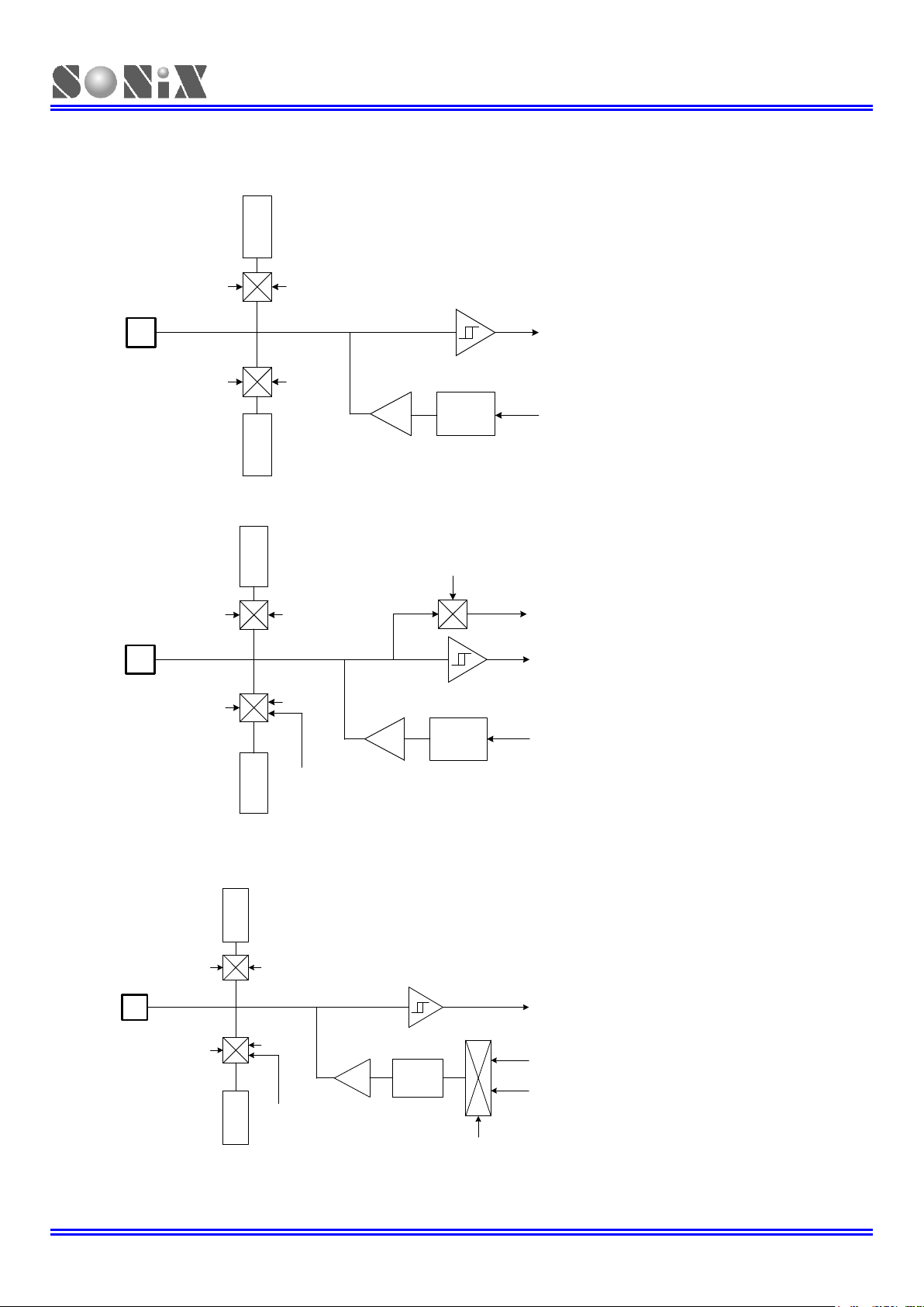
SN32F100 Series
RPU
Output
Latch
Pin
GPIOn_CFG
I/O Input Bus
I/O Output Bus
GPIOPn_MODE
RPD
GPIOn_CFGGPIOPn_MODE
RPU
Output
Latch
Pin
GPIOn_CFG
I/O Input Bus
Output Bus
GPIOPn_MODE
RPD
GPIOn_CFG
GPIOPn_MODE
Specific Input Bus
Specific Input Function Control Bit
*. Specific Output
Function Control Bit
*. Some specific functions switch I/O direction directly, not through GPIOn_MODE register.
RPU
Output
Latch
Pin
GPIOn_CFG
I/O Input Bus
Output Bus
GPIOPn_MODE
RPD
GPIOn_CFG
GPIOPn_MODE
Specific Output Bus
Specific Input Function Control Bit
*. Specific Output
Function Control Bit
*. Some specific functions switch I/O direction directly, not through GPIOn_MODE register.
32-Bit Cortex-M0 Micro-Controller
1.6 PIN CIRCUIT DIAGRAMS
Normal Bi-direction I/O Pin.
Bi-direction I/O Pin Shared with Specific Digital Input Function, e.g. SPI, I2C…
Bi-direction I/O Pin Shared with Specific Digital Output Function, e.g. SPI, I2C…
SONiX TECHNOLOGY CO., LTD Page 25 Version 1.9
Page 26
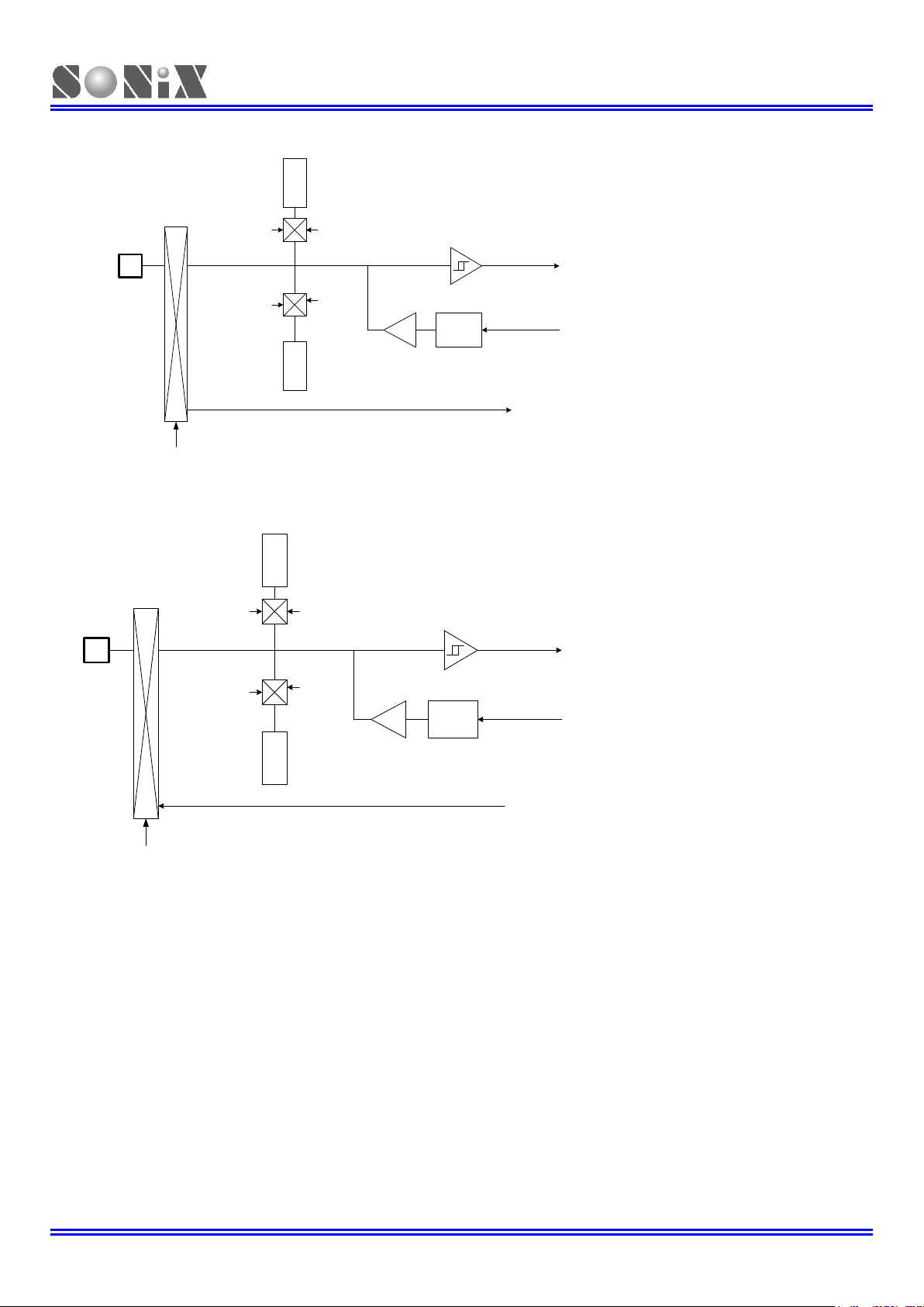
SN32F100 Series
RPU
Output
Latch
Pin
GPIOn_CFG
I/O Input Bus
I/O Output Bus
GPIOPn_MODE
RPD
GPIOn_CFG
GPIOPn_MODE
*. Specific Output Function Control Bit
*. Some specific functions switch I/O direction directly, not through GPIOn_MODE register.
Analog IP Input Terminal
RPU
Output
Latch
Pin
GPIOn_CFG
I/O Input Bus
I/O Output Bus
GPIOPn_MODE
RPD
GPIOn_CFG
GPIOPn_MODE
*. Specific Output Function Control Bit
*. Some specific functions switch I/O direction directly, not through GPIOn_MODE register.
Analog IP Output Terminal
32-Bit Cortex-M0 Micro-Controller
Bi-direction I/O Pin Shared with Specific Analog Input Function, e.g. XIN, ADC…
Bi-direction I/O Pin Shared with Specific Analog Output Function, e.g. XOUT…
SONiX TECHNOLOGY CO., LTD Page 26 Version 1.9
Page 27
SN32F100 Series
2
2
2
0x0000 0000
0x0001 0000
64 KB on-chip FLASH
0x1FFF 2000
Reserved
8 KB SRAM
Reserved
0x4000 0000
0x4008 0000
Peripheral
Reserved for Peripheral
0x6000 0000
Reserved for External
0xA000 0000
Reserved for External Device
0xE000 0000
Private Peripheral Bus
0xE010 0000
Reserved
0xFFFF FFFF
0x4000 0000
0x4000 2000
0x4000 4000
0x4000 6000
0x4000 8000
0x4001 0000
0x4001 2000
0x4001 4000
WDT
0x4001 6000
0x4001 8000
0x4001 C000
Reserved
Reserved
Reserved
Reserved
I2C0
0x4004 4000
0x4004 6000
0x4004 8000
GPIO2
GPIO3
GPIO0
GPIO1
Reserved
0x4008 0000
0xE000 0000
0xE010 0000
0xE000 ED00
0xE000 F000
Reserved
NVIC
Debug Control
0xE000 E000
Reserved
SSP0
UART0
SYS0
SSP1
UART1
0x4006 0000
FMC
Reserved
CT16B0
CT16B1
CT32B0
CT32B1
I2S
RTC
PMU
0x4006 4000
0x4006 2000
0x4005 6000
0x4004 C000
0x4004 A000
0x4003 2000
0x4001 E000
Reserved
0x4001 A000
0x4003 4000
0x4005 8000
0x4005 A000
0x1FFF 0000
0x1FFF 1000
0x2000 0000
0x2000 2000
4 KB Boot ROM
Reserved
0x1FFF 2800
SYS1
0x4005 E000
I2C1
0x4005 C000
Sigma-delta DAC
Comparator
Sigma-delta ADC
0x4006 5000
0x4006 6000
0x4006 8000
32-Bit Cortex-M0 Micro-Controller
CENTRAL PROCESSOR UNIT (CPU)
2.1 MEMORY MAP
SONiX TECHNOLOGY CO., LTD Page 27 Version 1.9
Page 28
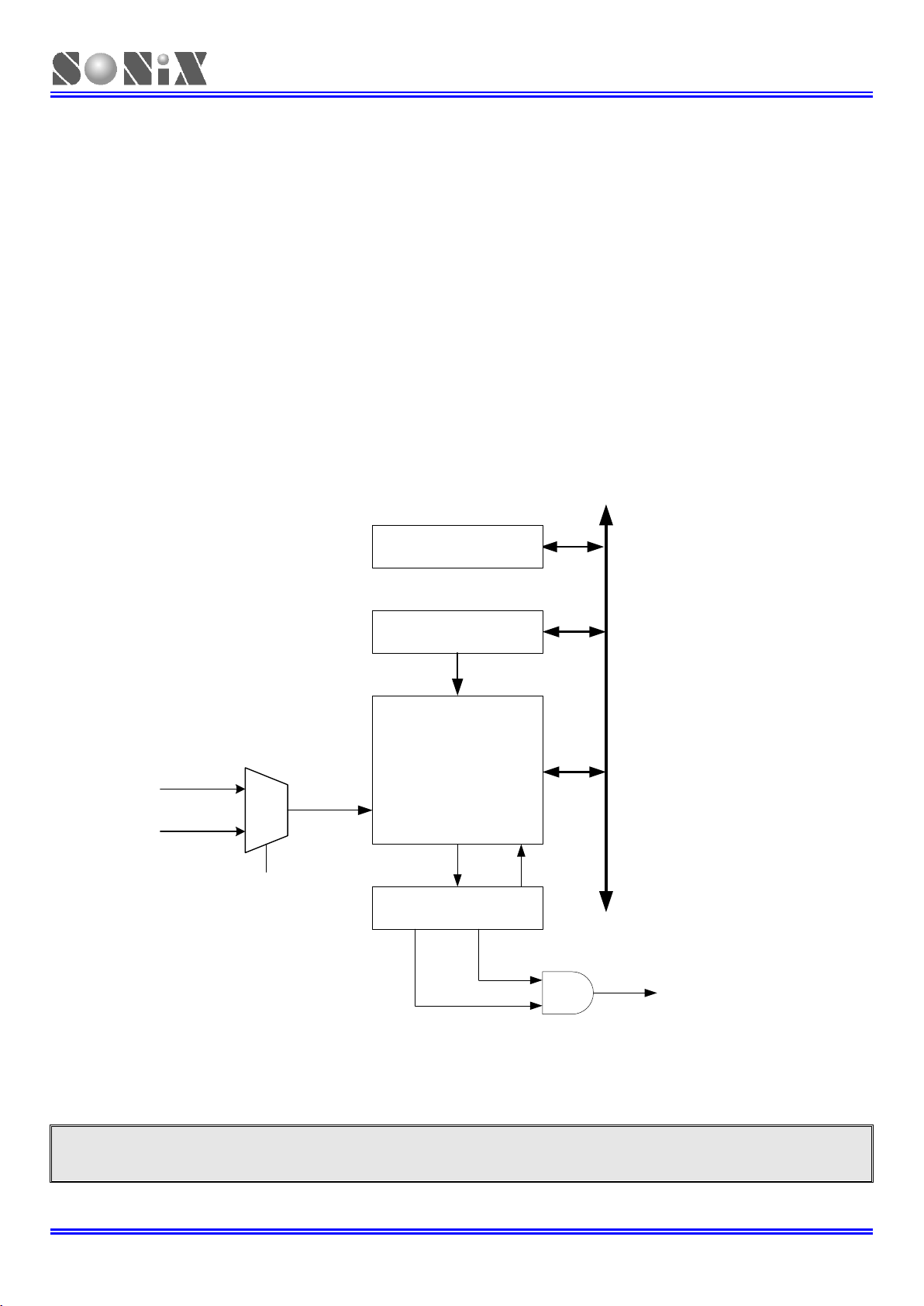
SN32F100 Series
SYSTICK_CALIB
SysTick interrupt
SYSTICK_LOAD
SYSTICK_VAL
24-bit down counter
CLKSOURCE
System clock
Ref. clock
(Fix to 1)
1
0
SYSTICK_CTRL
clock
Load data
Private
Peripheral
Bus
ENABLE
COUNTFLAG TICKINT
Note: When the processor is halted for debugging the counter does not decrease.
32-Bit Cortex-M0 Micro-Controller
2.2 SYSTEM TICK TIMER
The SysTick timer is an integral part of the Cortex-M0. The SysTick timer is intended to generate a fixed 10-ms
interrupt for use by an operating system or other system management software.
Since the SysTick timer is a part of the Cortex-M0, it facilitates porting of software by providing a standard timer that is
available on Cortex-M0 based devices.
Refer to the Cortex-M0 User Guide for details.
2.2.1 OPERATION
The SysTick timer is a 24-bit timer that counts down to zero and generates an interrupt.
The intent is to provide a fixed 10-ms time interval between interrupts. The system tick timer is enabled through the
SysTick control register. The system tick timer clock is fixed to the frequency of the system clock.
The block diagram of the SysTick timer:
When SysTick timer is enabled, the timer counts down from the current value (SYST_VAL) to zero, reloads to the value
in the SysTick Reload Value Register (SYST_LOAD) on the next clock edge, then decrements on subsequent clocks.
When the counter transitions to zero, the COUNTFLAG status bit is set to 1. The COUNTFLAG bit clears on reads.
SONiX TECHNOLOGY CO., LTD Page 28 Version 1.9
Page 29
SN32F100 Series
Bit
Name
Description
Attribute
Reset
31:17
Reserved
R
0
16
COUNTFLAG
This flag is set when the System Tick counter counts down to 0, and is
cleared by reading this register.
R/W
0
15:3
Reserved
R
0
2
CLKSOURCE
Selects the SysTick timer clock source.
0: reference clock.
1: system clock. (Fixed)
R
1
1
TICKINT
System Tick interrupt enable.
0: Disable the System Tick interrupt
1: Enable the System Tick interrupt, the interrupt is generated when the
System Tick counter counts down to 0.
R/W
0
0
ENABLE
System Tick counter enable.
0: Disable
1: Enable
R/W
0
Bit
Name
Description
Attribute
Reset
31:24
Reserved
R
0
23:0
RELOAD
Value to load into the SYST_CVR when the counter is enabled and when
it reaches 0.
R/W
0x5F7F9B
32-Bit Cortex-M0 Micro-Controller
2.2.2 SYSTICK USAGE HINTS AND TIPS
The interrupt controller clock updates the SysTick counter. Some implementations stop this clock signal for low power
mode. If this happens, the SysTick counter stops.
Ensure SW uses word accesses to access the SysTick registers.
The SysTick counter reload and current value are not initialized by HW. This means the correct initialization sequence
for the SysTick counter is:
1. Program the reload value in SYSTICK_LOAD register.
2. Clear the current value by writing any value to SYSTICK_VAL register.
3. Program the Control and Status (SYSTICK_CTRL) register.
2.2.3 SYSTICK REGISTERS
2.2.3.1 System Tick Timer Control and Status register (SYSTICK_CTRL)
Address: 0xE000 E010 (Refer to Cortex-M0 Spec)
2.2.3.2 System Tick Timer Reload value register (SYSTICK_LOAD)
Address: 0xE000 E014 (Refer to Cortex-M0 Spec)
The RELOAD register is set to the value that will be loaded into the SysTick timer whenever it counts down to zero.
This register is set by software as part of timer initialization. The SYST_CALIB register may be read and used as the
value for RELOAD if the CPU or external clock is running at the frequency intended for use with the SYST_CALIB
value.
The following example illustrates selecting the SysTick timer reload value to obtain a 10 ms time interval with the
system clock set to 50 MHz.
The SysTick clock = system clock = 50 MHz
RELOAD = (system tick clock frequency × 10 ms) −1 = (50 MHz × 10 ms) −1
= 0x0007A11F.
SONiX TECHNOLOGY CO., LTD Page 29 Version 1.9
Page 30
SN32F100 Series
Bit
Name
Description
Attribute
Reset
31:24
Reserved
R
0
23:0
CURRENT
Reading this register returns the current value of the System Tick counter.
Writing any value clears the System Tick counter and the COUNTFLAG
bit in SYST_CSR.
R/W
0x7E7F35
Bit
Name
Description
Attribute
Reset
31
NOREF
Indicates the reference clock to M0 is provided or not.
1: No reference clock provided.
R
1
30
SKEW
Indicates whether the TENMS value is exact, an inexact TENMS value
can affect the suitability of SysTick as a software real time clock.
0: TENMS value is exact
1: TENMS value is inexact, or not given.
R
0
29:24
Reserved
R
0
23:0
TENMS
Reload value for 10ms timing, subject to system clock skew errors. If the
value reads as zero, the calibration value is not known.
R/W
0xA71FF
32-Bit Cortex-M0 Micro-Controller
2.2.3.3 System Tick Timer Current Value register (SYSTICK_VAL)
Address: 0xE000 E018 (Refer to Cortex-M0 Spec)
2.2.3.4 System Tick Timer Calibration Value register (SYST_CALIB)
Address: 0xE000 E01C (Refer to Cortex-M0 Spec)
SONiX TECHNOLOGY CO., LTD Page 30 Version 1.9
Page 31

SN32F100 Series
Execution No.
Priority
Function
Description
Address Offset
0
-
-
Reserved
0x0000 0000
1
-3
Reset
Reset
0x0000 0004
2
-2
NMI_Handler
Non maskable interrupt.
0x0000 0008
3
-1
HardFault_Handler
All class of fault
0x0000 000C
4~10
Reserved
Reserved
Reserved
-
11
Settable
SVCCall
0x0000 002C
12~13
Reserved
Reserved
Reserved
-
14
Settable
PendSV 0x0000 0038
15
Settable
SysTick 0x0000 003C
16
Settable
IRQ0/P0IRQ
GPIO interrupt status of port 0
0x0000 0040
17
Settable
IRQ1/P1IRQ
GPIO interrupt status of port 1
0x0000 0044
18
Settable
IRQ2/P2IRQ
GPIO interrupt status of port 2
0x0000 0048
19
Settable
IRQ3/P3IRQ
GPIO interrupt status of port 3
0x0000 004C
20~32
Reserved
Reserved
Reserved
-
33
Settable
IRQ17/CMPIRQ
CMP
0x0000 0084
34
Settable
IRQ18/CT16B0IRQ
CT16B0
0x0000 0088
35
Settable
IRQ19/CT16B1IRQ
CT16B1
0x0000 008C
36
Settable
IRQ20/CT32B0IRQ
CT32B0
0x0000 0090
37
Settable
IRQ21/CT32B1IRQ
CT32B1
0x0000 0094
38
Settable
IRQ22/I2SIRQ
I2S
0x0000 0098
39
Settable
IRQ23/SSP0IRQ
SSP0
0x0000 009C
40
Settable
IRQ24/SSP1IRQ
SSP1
0x0000 00A0
41
Settable
IRQ25/UART0IRQ
UART0
0x0000 00A4
42
Settable
IRQ26/UART1IRQ
UART1
0x0000 00A8
32-Bit Cortex-M0 Micro-Controller
2.3 NESTED VECTORED INTERRUPT CONTROLLER (NVIC)
All interrupts including the core exceptions are managed by the NVIC. NVIC has the following Features:
The NVIC supports 32 vectored interrupts.
4 programmable interrupt priority levels with hardware priority level masking.
Low-latency exception and interrupt handling.
Efficient processing of late arriving interrupts.
Implementation of System Control Registers
Software interrupt generation.
2.3.1 INTERRUPT AND EXCEPTION VECTORS
2.3.2 NVIC REGISTERS
SONiX TECHNOLOGY CO., LTD Page 31 Version 1.9
Page 32

SN32F100 Series
43
Settable
IRQ27/I2C0IRQ
I2C0
0x0000 00AC
44
Settable
IRQ28/I2C1IRQ
I2C1
0x0000 00B0
45
Settable
IRQ29/WDTIRQ
WDT
0x0000 00B4
46
Settable
IRQ30/LVDIRQ
LVD
0x0000 00B8
47
Settable
IRQ31/RTCIRQ
RTC
0x0000 00BC
Bit
Name
Description
Attribute
Reset
31:0
SETENA[31:0]
Interrupt set-enable bits.
Write 0: No effect
1: Enable interrupt.
Read 0: Interrupt disabled
1: Interrupt enabled.
R/W
0
Bit
Name
Description
Attribute
Reset
31:0
CLRENA[31:0]
Interrupt clear-enable bits.
Write 0: No effect
1: Disable interrupt.
Read 0: Interrupt disabled
1: Interrupt enabled.
R/W
0
Bit
Name
Description
Attribute
Reset
31:0
SETPEND[31:0]
Interrupt set-pending bits.
Write 0: No effect
1: Change interrupt state to pending
Read 0: Interrupt is not pending
1: Interrupt is pending
R/W
0
32-Bit Cortex-M0 Micro-Controller
2.3.2.1 IRQ0~31 Interrupt Set-Enable Register (NVIC_ISER)
Address: 0xE000 E100 (Refer to Cortex-M0 Spec.)
The ISER enables interrupts, and shows the interrupts that are enabled.
2.3.2.2 IRQ0~31 Interrupt Clear-Enable Register (NVIC_ICER)
Address: 0xE000 E180 (Refer to Cortex-M0 Spec.)
The ICER disables interrupts, and shows the interrupts that are enabled.
2.3.2.3 IRQ0~31 Interrupt Set-Pending Register (NVIC_ISPR)
Address: 0xE000 E200 (Refer to Cortex-M0 Spec.)
The ISPR forces interrupts into the pending state, and shows the interrupts that are pending.
Note: Writing 1 to the ISPR bit corresponding to
an interrupt that is pending has no effect
a disabled interrupt sets the state of that interrupt to pending.
2.3.2.4 IRQ0~31 Interrupt Clear-Pending Register (NVIC_ICPR)
Address: 0xE000 E280 (Refer to Cortex-M0 Spec.)
The ICPR removes the pending state from interrupts, and shows the interrupts that are pending.
Note: Writing 1 to an ICPR bit does not affect the active state of the corresponding interrupt.
SONiX TECHNOLOGY CO., LTD Page 32 Version 1.9
Page 33

SN32F100 Series
Bit
Name
Description
Attribute
Reset
31:0
CLRPEND[31:0]
Interrupt clear-pending bits.
Write 0: No effect
1: Removes pending state of an interrupt
Read 0: Interrupt is not pending
1: Interrupt is pending
R/W
0
Bit
Name
Description
Attribute
Reset
31:24
PRI_(4*n+3)
Each priority field holds a priority value, 0-192. The lower the value, the
greater the priority of the corresponding interrupt. The processor implements
only bits[31:30] of each field, bits [29:24] read as zero and ignore writes. This
means writing 255 to a priority register saves value 192 to the register.
R/W
0
23:16
PRI_(4*n+2)
Each priority field holds a priority value, 0-192. The lower the value, the
greater the priority of the corresponding interrupt. The processor implements
only bits[23:22] of each field, bits [21:16] read as zero and ignore writes. This
means writing 255 to a priority register saves value 192 to the register.
R/W
0
15:8
PRI_(4*n+1)
Each priority field holds a priority value, 0-192. The lower the value, the
greater the priority of the corresponding interrupt. The processor implements
only bits[15:14] of each field, bits [13:8] read as zero and ignore writes. This
means writing 255 to a priority register saves value 192 to the register.
R/W
0
7:0
PRI_4*n
Each priority field holds a priority value, 0-192. The lower the value, the
greater the priority of the corresponding interrupt. The processor implements
only bits[7:6] of each field, bits [5:0] read as zero and ignore writes. This
means writing 255 to a priority register saves value 192 to the register.
R/W
0
Note: To write to this register, user must write 0x05FA to the VECTKEY field at the same time, otherwise
the processor ignores the write.
Bit
Name
Description
Attribute
Reset
31:16
VECTKEY
Register key.
Read as unknown. Write 0x05FA to VECTKEY, otherwise the write is
ignored.
R/W
0
15
ENDIANESS
Data endianness implemented
0: Little-endian
1: Big-endian
R
0
14:3
Reserved
R
0
2
SYSRESETREQ
System reset request. This bit read as 0.
0: No effect
1: Requests a system level reset.
W
0
1
VECTCLRACTIVE
Reserved for debug use. This bit read as 0. When writing to the register
you must write 0 to this bit, otherwise behavior is Unpredictable.
W
0
32-Bit Cortex-M0 Micro-Controller
2.3.2.5 IRQ0~31 Interrupt Priority Register (NVIC_IPRn) (n=0~7)
Address: 0xE000 E400 + 0x4 * n (Refer to Cortex-M0 Spec.)
The interrupt priority registers provide an 8-bit priority field for each interrupt, and each register holds four priority fields.
This means the number of registers is implementation-defined, and corresponds to the number of implemented
interrupts.
2.4 APPLICATION INTERRUPT AND RESET CONTROL (AIRC)
Address: 0xE000 ED0C (Refer to Cortex-M0 Spec)
The entire MCU, including the core, can be reset by SW by setting the SYSRESREQ bit in the AIRC register in
Cortex-M0 spec.
SONiX TECHNOLOGY CO., LTD Page 33 Version 1.9
Page 34

SN32F100 Series
0
Reserved
R
0
32-Bit Cortex-M0 Micro-Controller
SONiX TECHNOLOGY CO., LTD Page 34 Version 1.9
Page 35

SN32F100 Series
Bit
Name
Description
Attribute
Reset
31:16
Code Security[15:0]
Code Security
0xFFFF: CS0
0x5A5A: CS1
0xA5A5: CS2
0x55AA: CS3
R/W
0xFFFF
15:4
Reserved
R 1
3:1
Reserved
R 0 0 Reserved
R 1
32-Bit Cortex-M0 Micro-Controller
2.5 CODE OPTION TABLE
Address: 0x1FFF 2000
SONiX TECHNOLOGY CO., LTD Page 35 Version 1.9
Page 36

SN32F100 Series
Register
Description (Refer to Cortex-M0 Spec)
R0~R12
General-purpose registers for data operations.
SP (R13)
The Stack Pointer (SP). In Thread mode, the CONTROL register indicates the stack pointer to use,
Main Stack Pointer (MSP) or Process Stack Pointer (PSP)
On reset, the processor loads the MSP with the value from address 0x00000000.
LR (R14)
The Link Register (LR). It stores the return information for subroutines, function calls, and exceptions.
PC (R15)
The Program Counter (PC). It contains the current program address.
On reset, the processor loads the PC with the value of the reset vector, at address 0x00000004.
PSR
The Program Status Register (PSR) combines:
• Application Program Status Register (APSR)
• Interrupt Program Status Register (IPSR)
• Execution Program Status Register (EPSR).
These registers are mutually exclusive bit fields in the 32-bit PSR.
PRIMASK
The PRIMASK register prevents activation of all exceptions with configurable priority.
CONTROL
The CONTROL register controls the stack used when the processor is in Thread mode.
32-Bit Cortex-M0 Micro-Controller
2.6 CORE REGISTER OVERVIEW
SONiX TECHNOLOGY CO., LTD Page 36 Version 1.9
Page 37

SN32F100 Series
3
3
3
VDD
VSS
VDD
VSS
Watchdog Normal Run
Watchdog Stop
System Normal Run
System Stop
LVD Detect Level
External Reset
Low Detect
External Reset
High Detect
Watchdog
Overflow
Watchdog
Reset Delay
Time
External
Reset Delay
Time
Power On
Delay Time
Power
External Reset
Watchdog Reset
System Status
32-Bit Cortex-M0 Micro-Controller
SYSTEM CONTROL
3.1 RESET
A system reset is generated when one of the following events occurs:
1. A low level on the RST pin (external reset).
2. Power-on reset (POR reset)
3. LVD reset
4. Watchdog Timer reset (WDT reset)
5. Software reset (SW reset)
6. DPDWAKEUP reset when exiting Deep power-down mode by DPDWAKEUP pin
The reset source can be identified by checking the reset flags in System Reset Status register (SYS0_RSTST).
These sources act on the RST pin and it is always kept low during the delay phase. The RESET service routine vector
is fixed at address 0x00000004 in the memory map. For more details, refer to Interrupt and Exception Vectors.
Finishing any reset sequence needs some time. The system provides complete procedures to make the power on reset
successful. For different oscillator types, the reset time is different. That causes the VDD rise rate and start-up time of
different oscillator is not fixed. RC type oscillator’s start-up time is very short, but the crystal type is longer. Under client
terminal application, users have to take care of the power on reset time for the master terminal requirement. The reset
timing diagram is as following.
3.1.1 POWER-ON RESET (POR)
The power on reset depends on LVD operation for most power-up situations. The power supplying to system is a rising
curve and needs some time to achieve the normal voltage. Power on reset sequence is as following:
Power-up: System detects the power voltage up and waits for power stable.
External reset (only external reset pin enable): System checks external reset pin status. If external reset pin is
not high level, the system keeps reset status and waits external reset pin released.
System initialization: All system registers is set as initial conditions and system is ready.
Oscillator warm up: Oscillator operation is successfully and supply to system clock.
Program executing: Power on sequence is finished and program executes from Boot loader.
SONiX TECHNOLOGY CO., LTD Page 37 Version 1.9
Page 38

SN32F100 Series
Note: Please refer to the “WATCHDOG TIMER” about watchdog timer detail information.
VDD
VSS
V1
V2
V3
System Work
Well Area
System Work
Error Area
32-Bit Cortex-M0 Micro-Controller
3.1.2 WATCHDOG RESET (WDT RESET)
Watchdog reset is a system protection. In normal condition, system works well and clears watchdog timer by program.
Under error condition, system is in unknown situation and watchdog can’t be clear by program before watchdog timer
overflow. Watchdog timer overflow occurs and the system is reset. After watchdog reset, the system restarts and
returns normal mode. Watchdog reset sequence is as following.
Watchdog timer status: System checks watchdog timer overflow status. If watchdog timer overflow occurs, the
system is reset.
System initialization: All system registers is set as initial conditions and system is ready.
Oscillator warm up: Oscillator operation is successfully and supply to system clock.
Program executing: Power on sequence is finished and program executes from 0x0.
Watchdog timer application note is as following.
Before clearing watchdog timer, check I/O status and check RAM contents can improve system error.
Don’t clear watchdog timer in interrupt vector and interrupt service routine. That can improve main routine fail.
Clearing watchdog timer program is only at one part of the program. This way is the best structure to enhance the
watchdog timer function.
3.1.3 BROWN-OUT RESET
3.1.3.1 BROWN OUT DESCRIPTION
The brown-out reset is a power dropping condition. The power drops from normal voltage to low voltage by external
factors (e.g. EFT interference or external loading changed). The brown out reset would make the system not work well
or executing program error.
Brown-Out Reset Diagram
The power dropping might through the voltage range that’s the system dead-band. The dead-band means the power
range can’t offer the system minimum operation power requirement. The above diagram is a typical b rown out reset
diagram. There is a serious noise under the VDD, and VDD voltage drops very deep. There is a dotted line to separate
the system working area. The above area is the system work well area. The below area is the system work error area
called dead-band. V1 doesn’t touch the below area and not affect the system operation. But the V2 and V3 is under the
below area and may induce the system error occurrence. Let system under dead-band includes some conditions.
DC application:
The power source of DC application is usually using battery. When low battery condition and MCU drive any loading,
the power drops and keeps in dead-band. Under the situation, the power won’t drop deeper and not touch the system
reset voltage. That makes the system under dead-band.
AC application:
SONiX TECHNOLOGY CO., LTD Page 38 Version 1.9
Page 39

SN32F100 Series
Vdd (V)
System Rate (Fcpu)
System Mini.
Operating Voltage.
System Reset
Voltage.
Dead-Band Area
Normal Operating
Area
Reset Area
Note: The “Zener diode reset circuit”, “Voltage bias reset circuit” and “External reset IC” can completely
improve the brown out reset, DC low battery and AC slow power down conditions.
32-Bit Cortex-M0 Micro-Controller
In AC power application, the DC power is regulated from AC power source. This kind of power usually couples with AC
noise that makes the DC power dirty. Or the external loading is very heavy, e.g. driving motor. The loading operating
induces noise and overlaps with the DC power. VDD drops by the noise, and the system works under unstable power
situation.
The power on duration and power down duration are longer in AC application. The system power on sequence protects
the power on successful, but the power down situation is like DC low battery condition. When turn off the AC power, the
VDD drops slowly and through the dead-band for a while.
3.1.3.2 THE SYSTEM OPERATING VOLTAGE DECSRIPTION
To improve the brown out reset needs to know the system minimum operating voltage which is depend on the system
executing rate and power level. Different system executing rates have different system minimum operating voltage. The
electrical characteristic section shows the system voltage to executing rate relationship.
Normally the system operation voltage area is higher than the system reset voltage to VDD, and the reset voltage is
decided by LVD detect level. The system minimum operating voltage rises when the system executing rate upper even
higher than system reset voltage. The dead-band definition is the system minimum operating voltage above the system
reset voltage.
3.1.3.3 BROWN-OUT RESET IMPROVEMENT
How to improve the brown reset condition? There are some methods to improve brown out reset as following.
LVD reset
Watchdog reset
Reduce the system executing rate
External reset circuit. (Zener diode reset circuit, Voltage bias reset circuit, External reset IC)
SONiX TECHNOLOGY CO., LTD Page 39 Version 1.9
Page 40

SN32F100 Series
VDD
VSS
System Normal Run
System Stop
LVD Detect Voltage
Power On
Delay Time
Power
System Status
Power is below LVD Detect
Voltage and System Reset.
32-Bit Cortex-M0 Micro-Controller
LVD reset:
The LVD (low voltage detector) is built-in SONiX 32-bit MCU to be brown out reset protection. When the VDD drops
and is below LVD detect voltage, the LVD asserts an interrupt signal to the NVIC. This signal can be enabled for
interrupt in the Interrupt Enable Register in the NVIC in order to cause a CPU interrupt; if not, SW can monitor the
signal by reading a dedicated status register. An additional threshold level can be selected to cause a forced reset of
the chip. The LVD detect level is different by each MCU. The LVD voltage level is a point of voltage and not easy to
cover all dead-band range. Using LVD to improve brown out reset is dependent on application requirement and
environment. If the power variation is very deep, violent and trigger the LVD, the LVD can be the protection. If the
power variation can touch the LVD detect level and make system work error, the LVD can’t be the protection an d need
to other reset methods. More detail LVD information is in the electrical characteristic section.
Watchdog reset:
The watchdog timer is a protection to make sure the system executes well. Normally the watchdog timer would be clear
at one point of program. Don’t clear the watchdog timer in several addresses. The system executes normally and the
watchdog won’t reset system. When the system is under dead-band and the execution error, the watchdog timer can’t
be clear by program. The watchdog is continuously counting until overflow occurrence. The overflow signal of
watchdog timer triggers the system to reset and return to normal mode after reset sequence. This method also can
improve brown out reset condition and make sure the system to return normal mode.
If the system reset by watchdog and the power is still in dead-band, the system reset sequence won’t be successful
and the system stays in reset status until the power return to normal range.
Reduce the system executing rate:
If the system rate is fast and the dead-band exists, to reduce the system executing rate can improve the dead-band.
The lower system rate is with lower minimum operating voltage. Select the power voltage that’s no dead-band issue
and find out the mapping system rate. Adjust the system rate to the value and the system exits the dead-band issue.
This way needs to modify whole program timing to fit the application requirement.
External reset circuit:
The external reset methods also can improve brown out reset and is the complete solution. There are three external
reset circuits to improve brown out reset including “Zener diode reset circuit”, “Voltage bias reset circuit” and “External
reset IC”. These three reset structures use external reset signal and control to make sure the MCU be reset under
power dropping and under dead-band. The external reset information is described in the next section.
3.1.4 EXTERNAL RESET
External reset function is controlled by External RESET pin control (SYS0_EXRSTCTRL) register. Default value is 1,
which means external reset function is enabled. External reset pin is Schmitt Trigger structure and low level active. The
system is running when reset pin is high level voltage input. The reset pin receives the low voltage and the system is
reset. The external reset operation actives in power on and normal running mode. During system power-up, the
external reset pin must be high level input, or the system keeps in reset status. External reset sequence is as following.
External reset (only external reset pin enable): System checks external reset pin status. If external reset pin is
System initialization: All system registers is set as initial conditions and system is ready.
Oscillator warm up: Oscillator operation is successfully and supply to system clock.
SONiX TECHNOLOGY CO., LTD Page 40 Version 1.9
not high level, the system keeps reset status and waits external reset pin released.
Page 41

SN32F100 Series
MCU
VDD
VSS
VCC
GND
R
S
T
R1
47K ohm
C1
0.1uF
R2
100 ohm
Note: The reset circuit is no any protection against unusual power or brown out reset.
MCU
VDD
VSS
VCC
GND
R
S
T
R1
47K ohm
C1
0.1uF
DIODE
R2
100 ohm
32-Bit Cortex-M0 Micro-Controller
Program executing: Power on sequence is finished and program executes from Boot loader.
The external reset can reset the system during power on duration, and good external reset circuit can protect the
system to avoid working at unusual power condition, e.g. brown out reset in AC power application.
3.1.4.1 SIMPLY RC RESET CIRCUIT
This is the basic reset circuit, and only includes R1 and C1. The RC circuit operation makes a slow rising signal into
reset pin as power up. The reset signal is slower than VDD power up timing, and system occurs a power on signal from
the timing difference.
3.1.4.2 DIODE & RC RESET CIRCUIT
This is the better reset circuit. The R1 and C1 circuit operation is like the simply reset circuit to make a power on signal.
The reset circuit has a simply protection against unusual power. The diode offers a power positive path to conduct
higher power to VDD. It is can make reset pin voltage level to synchronize with VDD voltage. The structure can
improve slight brown out reset condition.
SONiX TECHNOLOGY CO., LTD Page 41 Version 1.9
Page 42

SN32F100 Series
Note: The R2 100 ohm resistor of “Simply reset circuit” and “Diode & RC reset circuit” is necessary to
limit any current flowing into reset pin from external capacitor C in the event of reset pin
breakdown due to Electrostatic Discharge (ESD) or Electrical Over-stress (EOS).
MCU
VDD
VSS
VCC
GND
R
S
T
R1
33K ohm
R3
40K ohm
R2
10K ohm
Vz
Q1
E
C
B
MCU
VDD
VSS
VCC
GND
R
S
T
R1
47K ohm
R3
2K ohm
R2
10K ohm
Q1
E
C
B
32-Bit Cortex-M0 Micro-Controller
3.1.4.3 ZENER DIODE RESET CIRCUIT
The Zener diode reset circuit is a simple low voltage detector and can improve brown out reset condition
completely. Use Zener voltage to be the active level. When VDD voltage level is above “Vz + 0.7V”, the C terminal of
the PNP transistor outputs high voltage and MCU operates normally. When VDD is below “Vz + 0.7V”, the C terminal of
the PNP transistor outputs low voltage and MCU is in reset mode. Decide the reset detect voltage by Zener
specification. Select the right Zener voltage to conform the application.
3.1.4.4 VOLTAGE BIAS RESET CIRCUIT
The voltage bias reset circuit is a low cost voltage detector and can improve brown out reset condition completely.
The operating voltage is not accurate as Zener diode reset circuit. Use R1, R2 bias voltage to be the active level. When
VDD voltage level is above or equal to “0.7V x (R1 + R2) / R1”, the C terminal of the PNP transistor outputs high
voltage and MCU operates normally. When VDD is below “0.7V x (R1 + R2) / R1”, the C terminal of the PNP transistor
SONiX TECHNOLOGY CO., LTD Page 42 Version 1.9
Page 43

SN32F100 Series
Note: Under unstable power condition as brown out reset, “Zener diode reset circuit” and “Voltage bias
reset circuit” can protects system no any error occurrence as power dropping. When power drops
below the reset detect voltage, the system reset would be triggered, and then system executes
reset sequence. That makes sure the system work well under unstable power situation.
MCU
VDD
VSS
VCC
GND
R
S
T
Reset
IC
VDD
VSS
RST
Bypass
Capacitor
0.1uF
32-Bit Cortex-M0 Micro-Controller
outputs low voltage and MCU is in reset mode.
Decide the reset detect voltage by R1, R2 resistances. Select the right R1, R2 value to conform the application. In the
circuit diagram condition, the MCU’s reset pin level varies with VDD voltage variation, and the differential voltage is
0.7V. If the VDD drops and the voltage lower than reset pin detect level, the system would be reset. If want to make the
reset active earlier, set the R2 > R1 and the cap between VDD and C terminal voltage is larger than 0.7V. The external
reset circuit is with a stable current through R1 and R2. For power consumption issue application, e.g. DC power
system, the current must be considered to whole system power consumption.
3.1.4.5 EXTERNAL RESET IC
The external reset circuit also uses external reset IC to enhance MCU reset performance. This is a high cost and good
effect solution. By different application and system requirement to select suitable reset IC. The reset circuit can improve
all power variation.
3.1.5 SOFTWARE RESET
The entire MCU, including the core, can be reset by software by setting the SYSRESREQ bit in the AIRC (Application
Interrupt and Reset Control) register in Cortex-M0 spec.
The software-initiated system reset sequence is as follows:
1. A software reset is initiated by setting the SYSRESREQ bit.
2. An internal reset is asserted.
3. The internal reset is deasserted and the MCU loads from memory the initial stack pointer, the initial program
counter, and the first instruction designated by the program counter, and then begins execution.
SONiX TECHNOLOGY CO., LTD Page 43 Version 1.9
Page 44

SN32F100 Series
Note: The ILRC can ONLY be switched on and off by HW.
32-Bit Cortex-M0 Micro-Controller
3.2 SYSTEM CLOCK
Different clock sources can be used to drive the system clock (SYSCLK):
12 MHz internal high speed RC (IHRC)
16 KHz internal low speed RC (ILRC)
PLL clock
High speed external (EHS) crystal clock
Low speed external (ELS) 32.768 KHz crystal
One clock sources can be used to drive the audio (I2S/Codec) clock (I2SMCLK):
Audio High speed external (AUEHS) crystal clock for audio
Each clock source can be switched on or off independently when it is not used, to optimize power consumption.
The micro-controller is a dual clock system. There are high-speed clock and low-speed clock. The high-speed clock is
generated from the external oscillator & on-chip PLL circuit. The low-speed clock is generated from on-chip low-speed
RC oscillator circuit (ILRC 16 KHz).
3.2.1 INTERNAL RC CLOCK SOURCE
3.2.1.1 Internal High-speed RC Oscillator (IHRC)
The internal high-speed oscillator is 12MHz RC type. The accuracy is ±2% under commercial condition.
The IHRC can be switched on and off using the IHRCEN bit in Analog Block Control register (SYS0_ANBCTRL).
3.2.1.2 Internal Low-speed RC Oscillator (ILRC)
The system low clock source is the internal low-speed oscillator built in the micro-controller. The low-speed oscillator
uses RC type oscillator circuit. The frequency is affected by the voltage and temperature of the system. In common
condition, the frequency of the RC oscillator is about 16 KHz.
SONiX TECHNOLOGY CO., LTD Page 44 Version 1.9
Page 45

SN32F100 Series
PFD LPF VCO
DIV
M
DIV
P
Fclkout
FvcoFclkin
DIV
F
32-Bit Cortex-M0 Micro-Controller
3.2.2 PLL
SN32F100 series MCU uses the PLL to create the clocks for the core and peripherals. The input frequency range is
10MHz to 25MHz. The input clock is divided down and fed to the Phase-Frequency Detector (PFD). This block
compares the phase and frequency of its inputs, and generates a control signal when phase and/ or frequency do not
match. The loop filter filters these control signals and drives the voltage controlled oscillator (VCO), which generates
the main clock and optionally two additional phases. The VCO frequency range is 156MHz to 320MHz. These clocks
are divided by P by the programmable post divider to create the output clock(s). The VCO output clock is then divided
by M by the programmable feedback divider to generate the feedback clock. The output signal of the phase-frequency
detector is also monitored by the lock detector, to signal when the PLL has locked on to the input clock.
The PLL settling time is 100 μs.
3.2.2.1 PLL Frequency selection
The PLL frequency equations:
F
VCO
F
CLKOUT
= F
CLKIN
= F
/ F * M
/ P
VCO
The PLL frequency is determined by the following parameters:
F
F
F
: Frequency from the PLLCLKSEL multiplexer.
CLKIN
: Frequency of the Voltage Controlled Oscillator (VCO); 156 to 320 MHz.
VCO
: Frequency of PLL output.
CLKOUT
P: System PLL post divider ratio, controlled by PSEL bits in PLL control register (SYS0_PLLCTRL).
F: System PLL front divider ratio, controlled by FSEL bits in PLL control register (SYS0_PLLCTRL).
M: System PLL feedback divider ratio, controlled by MSEL bits in PLL control register (SYS0_PLLCTRL).
To select the appropriate values for M, P, and F, it is recommended to follow these constraints:
1. 10MHz ≤ F
2. 150MHz ≤ F
3. 2 < M ≤31
4. F = 1, or 2
5. P = 6, 8, 10, 12, or 14 (duty 50% +/- 2.5%)
6. F
= 20MHz, 30MHz, 40MHz, 50MHz, 24MHz, 36MHz, 48MHz, 32MHz, 22MHz, 24MHz, 50MHz
CLKOUT
≤ 25MHz
CLKIN
≤ 330MHz
VCO
with jitter < ±500 ps
SONiX TECHNOLOGY CO., LTD Page 45 Version 1.9
Page 46

SN32F100 Series
MCU
VCC
GND
C
20pF
XIN
X
O
U
T
VDD
VSS
C
20pF
CRYSTAL
Note: Connect the Crystal/Ceramic and C as near as possible to the XIN/XOUT/VSS pins of MCU.
Oscillator Mode
XTALIN pin
XTALOUT pin
IHRC
GPIO
GPIO
EHS X’TAL
Crystal/Ceramic
Crystal/Ceramic
4MHz Ceramic
4MHz Crystal
32-Bit Cortex-M0 Micro-Controller
3.2.3 EXTERNAL CLOCK SOURCE
3.2.3.1 External High-speed (EHS) Clock
External high clock includes Crystal/Ceramic modules. The startup time of is longer. The oscillator start-up time
decides reset time length.
3.2.3.2 CRYSTAL/CERAMIC
Crystal/Ceramic devices are driven by XIN, XOUT pins. For high/normal/low frequency, the driving currents are
different.
Structure: 1MHz~25MHz EHS external crystal/ceramic resonator
Main Purpose: System high clock source, RTC clock source, and PLL clock source.
Warm-up Time: 2048*F
XIN/XOUT Shared Pin Selection:
EHS
SONiX TECHNOLOGY CO., LTD Page 46 Version 1.9
Page 47

SN32F100 Series
Note: Connect the Crystal/Ceramic and C as near as possible to the AUXTALIN/AUXTALOUT/VSS pins of
MCU.
Oscillator Mode
AUXTALIN pin
AUXTALOUT pin
--
GPIO
GPIO
AUEHS X’TAL
Crystal/Ceramic
Crystal/Ceramic
32-Bit Cortex-M0 Micro-Controller
The resonator and the load capacitors have to be placed as close as possible to the oscillator pins in order to minimize
output distortion and startup stabilization time. The loading capacitance values must be adjusted according to the
selected oscillator.
The EHS crystal is switched on and off using the EHSEN bit in Analog Block Control register (SYS0_ANBCTRL).
3.2.3.3 Audio External High-speed (AUEHS) Clock
Structure: 1MHz~25MHz AUEHS external crystal/ceramic resonator
Main Purpose: Audio high clock source.
Warm-up Time: 2048*F
AUXTALIN/AUXTALOUT Shared Pin Selection:
AUEHS
The resonator and the load capacitors have to be placed as close as possible to the oscillator pins in order to minimize
output distortion and startup stabilization time. The loading capacitance values must be adjusted according to the
selected oscillator.
The AUEHS crystal is switched on and off using the AUEHSEN bit in Analog Block Control register (SYS0_ANBCTRL).
3.2.3.4 External Low-speed (ELS) Clock
The low-speed oscillator can use 32768 crystal oscillator circuit.
3.2.3.5 CRYSTAL
Crystal devices are driven by LXIN, LXOUT pins. The 32768 crystal and 10pF capacitor must be as near as possible to
MCU. The ELS crystal is switched on and off using the ELSEN bit in Analog Block Control register (SYS0_ANBCTRL).
SONiX TECHNOLOGY CO., LTD Page 47 Version 1.9
Page 48

SN32F100 Series
Note: Connect the Crystal/Ceramic and C as near as possible to the LXIN/LXOUT/VSS pins of MCU. The
capacitor between LXIN/LXOUT and VSS must be 10pF.
Clock Source
H/W Configuration
Description
External clock source
(Bypass)
In Bypass mode, the external clock signal
(square, sinus or triangle) with ~50% duty
cycle must be provided to drive the XTALIN/
LXTALIN pin while the XTALOUT/
LXTALOUT pin should be the inverse of
the input clock signal.
EHS X’tal can have a frequency of up to 25
MHz. Select this mode by setting EHSEN bit
in Analog Block Control register
(SYS0_ANBCTRL).
ELS X’TAL must have a frequency of 32.768
KHz. You select this mode by setting
ELSEN bit in Analog Block Control register
(SYS0_ANBCTRL).
External X’TAL
(EHS/ELS X’TAL)
The 1 to 25 MHz EHS X’TAL has the
advantage of producing a very accurate rate
on the main clock
ELS X’TAL must have a frequency of 32.768
KHz.
MCU
VCC
GND
C
10pF
LXIN
L
XOU
T
VDD
VSS
C
10pF
32768Hz
32-Bit Cortex-M0 Micro-Controller
3.2.3.6 Bypass Mode
SONiX TECHNOLOGY CO., LTD Page 48 Version 1.9
Page 49

SN32F100 Series
32-Bit Cortex-M0 Micro-Controller
3.2.4 SYSTEM CLOCK (SYSCLK) SELECTION
After a system reset, the IHRC is selected as system clock. When a clock source is used directly or through the PLL as
system clock, it is not possible to stop it.
A switch from one clock source to another occurs only if the target clock source is ready (clock stable after startup
delay or PLL locked). If a clock source which is not yet ready is selected, the switch will occur when the clock source is
ready.
Ready bits in SYS0_CSST register indicate which clock(s) is (are) ready and SYSCLKST bits in SYS0_CLKCFG
register indicate which clock is currently used as system clock.
3.2.5 CLOCK-OUT CAPABITITY
The MCU clock output (CLKOUT) capability allows the clock to be output onto the external CLKOUT pin. The
configuration registers of the corresponding GPIO port must be programmed in alternate function mode.
One of 6 clock signals can be selected as clock output:
1. HCLK
2. IHRC
3. ILRC
4. PLL clock output
5. ELS X’TAL
6. EHS X’TAL
7. AUEHS X’TAL
The selection is controlled by the CLKOUTSEL bits in SYS1_AHBCLKEN register.
SONiX TECHNOLOGY CO., LTD Page 49 Version 1.9
Page 50

SN32F100 Series
Note: EHSEN / ELSEN / IHRCEN bit can NOT be cleared if the EHS X’tal / ELS X’tal / IHRC is selected as
system clock or is selected to become the system clock.
Bit
Name
Description
Attribute
Reset
31:10
Reserved
R
0
9
AUEHSFREQ
Frequency range of AUEHS X’TAL
0: <=12MHz
1: >12MHz
R/W
0 8 AUEHSEN
Audio external high-speed clock enable
0: Disable AUEHS X’TAL.
1: Enable AUEHS X’TAL.
R/W
0
7:6
Reserved
R
0
5
EHSFREQ
Frequency range (driving ability) of EHS X’TAL
0: <=12MHz
1: >12MHz
R/W
0 4 EHSEN
External high-speed clock enable
0: Disable EHS X’TAL.
1: Enable EHS X’TAL.
R/W
0
3
Reserved
R
0
2
ELSEN
External low-speed oscillator enable
0: Disable External 32.768 KHz oscillator
1: Enable External 32.768 KHz oscillator
R/W
0
1
Reserved
R
0
0
IHRCEN
Internal high-speed clock enable
0: Disable internal 12 MHz RC oscillator.
1: Enable internal 12 MHz RC oscillator.
R/W
1
Note: PLLEN bit can NOT be cleared if the PLL is selected as system clock or is selected to become the
system clock.
Bit
Name
Description
Attribute
Reset
31:16
Reserved
R
0
15
PLLEN
PLL enable
0: Disable
1: Enable
R/W
0
14
Reserved
R
0
32-Bit Cortex-M0 Micro-Controller
3.3 SYSTEM CONTROL REGISTERS 0
Base Address: 0x4006 0000
3.3.1 Analog Block Control register (SYS0_ANBCTRL)
Address Offset: 0x00
Reset value: 0x0000 0001
3.3.2 PLL control register (SYS0_PLLCTRL)
Address Offset: 0x04
SONiX TECHNOLOGY CO., LTD Page 50 Version 1.9
Page 51

SN32F100 Series
13:12
PLLCLKSEL[1:0]
System PLL clock source
00: IHRC 12 MHz oscillator
01: EHS X’TAL 10 MHz ~ 25 MHz
Other: Reserved
R/W
0
11:9
Reserved
R
0
8
FSEL
Front divider value. The division value F is the programmed 2
FSEL
0: F = 1
1: F = 2
R/W
0
7:5
PSEL[2:0]
Post divider value. P= PSEL[2:0]*2
000~010: Reserved
011: P = 6
100: P = 8
101: P = 10
110: P = 12
111: P = 14
R/W
011b
4:0
MSEL[4:0]
Feedback divider value.
M: 3~31
R/W
0x3
Fclkout
Fclkin
V V V V
V V V
V V
V
V
V
44MHz
48MHz
16MHz
22MHz
16MHz
12MHz
12MHz
20MHz
30MHz
40MHz
22MHz
24MHz
25MHz
10MHz
10MHz
50MHz
24MHz
25MHz
32MHz
36MHz
F
CLKIN
(MHz)
FSEL
F=2
FEL
MSEL[4:0]=M
F
VCO
(MHz)
=F
CLKIN
/F*M
PSEL[2:0]
P= PSEL[2:0]*2
F
CLKOUT
(MHz)
10
0 1 20
200 5 10
20
10
0 1 22
220 5 10
22
10
0 1 18
180 3 6
30
10
0 1 24
240 3 6
40
10
0 1 30
300 3 6
50
12
0 1 16
192 4 8
24
12
0 1 18
216 3 6
36
12
0 1 24
288 3 6
48
16
0 1 16
256 4 8
32
16
0 1 18
288 3 6
48
20
1 2 30
300 3 6
50
22
0 1 12
264 3 6
44
24
0 1 12
288 3 6
48
25
0 1 12
300 3 6
50
32-Bit Cortex-M0 Micro-Controller
To select the appropriate values for M, P, and F, it is recommended to follow these constraints:
1. 10MHz ≤ F
2. 150MHz ≤ F
3. 2 < M ≤31
4. F = 1, or 2
5. P = 6, 8, 10, 12, or 14 (duty 50% +/- 2.5%)
6. F
= 20MHz, 30MHz, 40MHz, 50MHz, 24MHz, 36MHz, 48MHz, 32MHz, 22MHz, 24MHz, 50MHz
CLKOUT
≤ 25MHz
CLKIN
≤ 330MHz
VCO
with jitter < ±500 ps
3.3.2.1 RECOMMEND FREQUENCY SETTING
F
VCO
F
CLKOUT
= F
CLKIN
= F
/ F * M
/ P
VCO
SONiX TECHNOLOGY CO., LTD Page 51 Version 1.9
Page 52

SN32F100 Series
Bit
Name
Description
Attribute
Reset
31:9
Reserved
R
0
8
AUEHSRDY
Audio external high-speed clock ready flag
0: AUEHS oscillator not ready
1: AUEHS oscillator ready
R
0
7
Reserved
R
0
6
PLLRDY
PLL clock ready flag
0: PLL unlocked
1: PLL locked
R
0
5
Reserved
R
0
4
EHSRDY
External high-speed clock ready flag
0: EHS oscillator not ready
1: EHS oscillator ready
R
0
3
Reserved
R
0
2
ELSRDY
External low-speed clock ready flag
0: EHS oscillator not ready
1: EHS oscillator ready
R
0
1
Reserved
R
0
0
IHRCRDY
IHRC ready flag
0: IHRC not ready
1: IHRC ready
R
1
Bit
Name
Description
Attribute
Reset
31:7
Reserved
R
0
6:4
SYSCLKST[2:0]
System clock switch status
Set and cleared by HW to indicate which clock source is used as system
clock.
000: IHRC is used as system clock
001: ILRC is used as system clock
010: EHS X’TAL is used as system clock
011: ELS X’TAL is used as system clock
100: PLL is used as system clock
Other: Reserved
R
0
3
Reserved
R
0
2:0
SYSCLKSEL[2:0]
System clock switch
Set and cleared by SW.
000: IHRC
001: ILRC
010: EHS X’TAL
011: ELS X’TAL
100: PLL output
Other: Reserved
R/W
0
Bit
Name
Description
Attribute
Reset
31:4
Reserved
R
0
32-Bit Cortex-M0 Micro-Controller
3.3.3 Clock Source Status register (SYS0_CSST)
Address Offset: 0x08
3.3.4 System Clock Configuration register (SYS0_CLKCFG)
Address Offset: 0x0C
3.3.5 AHB Clock Prescale register (SYS0_AHBCP)
Address Offset: 0x10
SONiX TECHNOLOGY CO., LTD Page 52 Version 1.9
Page 53

SN32F100 Series
3:0
AHBPRE[3:0]
AHB clock source prescale value
0000: SYSCLK / 1
0001: SYSCLK / 2
0010: SYSCLK / 4
0011: SYSCLK / 8
0100: SYSCLK / 16
0101: SYSCLK / 32
0110: SYSCLK / 64
0111: SYSCLK / 128
1000: SYSCLK / 256
1001: SYSCLK / 512
Other: Reserved
R/W
0
Bit
Name
Description
Attribute
Reset
31:5
Reserved
R
0
4
PORRSTF
POR reset flag
Set by HW when a POR reset occurs.
0: ReadNo POR reset occurred
WriteClear this bit
1: POR reset occurred.
R/W
1
3
EXTRSTF
External reset flag
Set by HW when a reset from the RESET pin occurs.
0: ReadNo reset from RESET pin occurred
WriteClear this bit
1: Reset from RESET pin occurred.
R/W
0
2
LVDRSTF
LVD reset flag
Set by HW when a LVD reset occurs.
0: ReadNo LVD reset occurred
WriteClear this bit
1: LVD reset occurred.
R/W
0
1
WDTRSTF
WDT reset flag
Set by HW when a WDT reset occurs.
0: ReadNo watchdog reset occurred
WriteClear this bit
1: Watchdog reset occurred.
R/W
0 0 SWRSTF
Software reset flag
Set by HW when a software reset occurs.
0: ReadNo software reset occurred
WriteClear this bit
1: Software reset occurred.
R/W
1
Bit
Name
Description
Attribute
Reset
31:16
Reserved
R
0
15
LVDEN
LVD enable
0: Disable
1: Enable
R/W
0
14
LVDRSTEN
LVD Reset enable
0: Disable
1: Enable
R/W
0
32-Bit Cortex-M0 Micro-Controller
3.3.6 System Reset Status register (SYS0_RSTST)
Address Offset: 0x14
This register contains the reset source except DPDWAKEUP reset, since the LPFLAG bit in PMU_CTRL register had
presented this case.
3.3.7 LVD Control register (SYS0_LVDCTRL)
Address Offset: 0x18
The LVD control register selects four separate threshold values for generating a LVD interrupt to the NVIC or LVD
reset.
SONiX TECHNOLOGY CO., LTD Page 53 Version 1.9
Page 54

SN32F100 Series
13:6
Reserved
R
0
5:4
LVDINTLVL[1:0]
LVD interrupt level
00: The interrupt assertion threshold voltage is 2.00V
01: The interrupt assertion threshold voltage is 2.40V
10: The interrupt assertion threshold voltage is 2.70V
11: The interrupt assertion threshold voltage is 3.00V
R/W
0
3:2
Reserved
R
0
1:0
LVDRSTLVL[1:0]
LVD reset level
00: The reset assertion threshold voltage is 2.00V
01: The reset assertion threshold voltage is 2.40V
10: The reset assertion threshold voltage is 2.70V
11: Reserved
R/W
0
32-Bit Cortex-M0 Micro-Controller
SONiX TECHNOLOGY CO., LTD Page 54 Version 1.9
Page 55

SN32F100 Series
Bit
Name
Description
Attribute
Reset
31:1
Reserved
R
0
0
RESETDIS
External RESET pin disable bit.
0: Enable external RESET pin. (P0.15 acts as RESET pin)
1: Disable. (P0.15 acts as GPIO pin)
R/W
0
Bit
Name
Description
Attribute
Reset
31:1
Reserved
R
0
0
SWDDIS
SWD pin disable bit.
0: Enable SWD pin. (P0.13 acts as SWDIO pin, P0.12 acts as SWCLK pin)
1: Disable. (P0.13 and P0.12 act as GPIO pins)
R/W
0
32-Bit Cortex-M0 Micro-Controller
3.3.8 External RESET Pin Control register (SYS0_EXRSTCTRL)
Address Offset: 0x1C
3.3.9 SWD Pin Control register (SYS0_SWDCTRL)
Address Offset: 0x20
SONiX TECHNOLOGY CO., LTD Page 55 Version 1.9
Page 56

SN32F100 Series
Note:
1. When the clock is disabled, the peripheral register values may not be readable by SW and the
value returned is always 0x0.
2. HW will replace GPIO with CLKOUT function directly if CLKOUTSEL is Not 0.
Bit
Name
Description
Attribute
Reset
31
Reserved
R
0
30:28
CLKOUTSEL[2:0]
Clock output source
000: Disable
001: HCLK
010: PLL clock output
011: ILRC clock
100: IHRC clock
101: ELS clock
110: EHS clock
111: AUEHS clock
R/W
0
27:25
Reserved
R
0
24
WDTCLKEN
Enables clock for WDT.
0: Disable
1: Enable
R/W
1
23
RTCCLKEN
Enables clock for RTC.
0: Disable
1: Enable
R/W
0
22
I2SCLKEN
Enables clock for I2S.
0: Disable
1: Enable
R/W
0
21
I2C0CLKEN
Enables clock for I2C0.
0: Disable
1: Enable
R/W
0
20
I2C1CLKEN
Enables clock for I2C1.
0: Disable
1: Enable
R/W
0
19:18
Reserved
R
0
17
UART1CLKEN
Enables clock for UART1.
0: Disable
1: Enable
R/W
0
16
UART0CLKEN
Enables clock for UART0.
0: Disable
1: Enable
R/W
0
15:14
Reserved
R
0
13
SSP1CLKEN
Enables clock for SSP1.
0: Disable
1: Enable
R/W
0
12
SSP0CLKEN
Enables clock for SSP0.
0: Disable
1: Enable
R/W
0
11
CMPCLKEN
Enables clock for Comparator.
0: Disable
1: Enable
R/W
0
32-Bit Cortex-M0 Micro-Controller
3.4 SYSTEM CONTROL REGISTERS 1
Base Address: 0x4005 E000
3.4.1 AHB Clock Enable register (SYS1_AHBCLKEN)
Address Offset: 0x00
The SYS_AHBCLKEN register enables the AHB clock to individual system and peripheral blocks.
SONiX TECHNOLOGY CO., LTD Page 56 Version 1.9
Page 57

SN32F100 Series
10
Reserved
R
0
9
CT32B1CLKEN
Enables clock for CT32B1.
0: Disable
1: Enable
R/W
0
8
CT32B0CLKEN
Enables clock for CT32B0.
0: Disable
1: Enable
R/W
0
7
CT16B1CLKEN
Enables clock for CT16B1.
0: Disable
1: Enable
R/W
0 6 CT16B0CLKEN
Enables clock for CT16B0.
0: Disable
1: Enable
R/W
0
5:4
Reserved
R
0
3
GPIOCLKEN
Enables clock for GPIO.
0: Disable
1: Enable
R/W
1
2:0
Reserved
R
0
Note: Must reset the corresponding peripheral with SYS1_PRST register after changing the prescale
value.
Bit
Name
Description
Attribute
Reset
31
Reserved
R
0
30:28
AUEHSPRE[2:0]
Audio external high clock source prescale value
000: AUEHS / 1
001: AUEHS / 2
010: AUEHS / 4
011: AUEHS / 8
100: AUEHS / 16
Other: Reserved
R/W
0
27
Reserved
R
0
26:24
SSP1PRE[2:0]
SSP1 clock source prescale value
000: HCLK / 1
001: HCLK / 2
010: HCLK / 4
011: HCLK / 8
100: HCLK / 16
Other: Reserved
R/W
0
23
Reserved
R
0
22:20
SSP0PRE[2:0]
SSP0 clock source prescale value
000: HCLK / 1
001: HCLK / 2
010: HCLK / 4
011: HCLK / 8
100: HCLK / 16
Other: Reserved
R/W
0
19
Reserved
R
0
18:16
CMPPRE[2:0]
Comparator clock source prescale value
000: HCLK / 1
001: HCLK / 2
010: HCLK / 4
011: HCLK / 8
100: HCLK / 16
Other: Reserved
R/W
0
15
Reserved
R
0
32-Bit Cortex-M0 Micro-Controller
3.4.2 APB Clock Prescale register 0 (SYS1_APBCP0)
Address Offset: 0x04
SONiX TECHNOLOGY CO., LTD Page 57 Version 1.9
Page 58

SN32F100 Series
14:12
CT32B1PRE[2:0]
CT32B1 clock source prescale value
000: HCLK / 1
001: HCLK / 2
010: HCLK / 4
011: HCLK / 8
100: HCLK / 16
Other: Reserved
R/W
0
11
Reserved
R
0
10:8
CT32B0PRE[2:0]
CT32B0 clock source prescale value.
000: HCLK / 1
001: HCLK / 2
010: HCLK / 4
011: HCLK / 8
100: HCLK / 16
Other: Reserved
R/W
0
7
Reserved
R
0
6:4
CT16B1PRE[2:0]
CT16B1 clock source prescale value
000: HCLK / 1
001: HCLK / 2
010: HCLK / 4
011: HCLK / 8
100: HCLK / 16
Other: Reserved
R/W
0
3
Reserved
R
0
2:0
CT16B0PRE[2:0]
CT16B0 clock source prescale value
000: HCLK / 1
001: HCLK / 2
010: HCLK / 4
011: HCLK / 8
100: HCLK / 16
Other: Reserved
R/W
0
Note: Must reset the corresponding peripheral with SYS1_PRST register after changing the prescale
value.
Bit
Name
Description
Attribute
Reset
31:28
CLKOUTPRE[3:0]
Clock-out source prescale value
0000: Clock-out source / 1
0001: Clock-out source / 2
0010: Clock-out source / 4
0011: Clock-out source / 8
0100: Clock-out source / 16
0101: Clock-out source / 32
0110: Clock-out source / 64
0111: Clock-out source / 128
1000: Clock-out source / 256
1001: Clock-out source / 512
Other: Reserved
R/W
0
27
Reserved
R
0
26:24
I2C1PRE[2:0]
I2C1 clock source prescale value
000: HCLK / 1
001: HCLK / 2
010: HCLK / 4
011: HCLK / 8
100: HCLK / 16
Other: Reserved
R/W
0
23
Reserved
R
0
32-Bit Cortex-M0 Micro-Controller
3.4.3 APB Clock Prescale register 1 (SYS1_APBCP1)
Address Offset: 0x08
SONiX TECHNOLOGY CO., LTD Page 58 Version 1.9
Page 59

SN32F100 Series
22:20
WDTPRE[2:0]
WDT clock source prescale value
000: WDT_PCLK = WDT clock source / 1
001: WDT_PCLK = WDT clock source / 2
010: WDT_PCLK = WDT clock source / 4
011: WDT_PCLK = WDT clock source / 8
100: WDT_PCLK = WDT clock source / 16
101: WDT_PCLK = WDT clock source / 32
Other: Reserved
R/W
0
19:15
Reserved
R
0
14:12
I2SPRE[2:0]
I2S clock source prescale value
000: HCLK / 1
001: HCLK / 2
010: HCLK / 4
011: HCLK / 8
100: HCLK / 16
Other: Reserved
R/W
0
11
Reserved
R
0
10:8
I2C0PRE[2:0]
I2C0 clock source prescale value
000: HCLK / 1
001: HCLK / 2
010: HCLK / 4
011: HCLK / 8
100: HCLK / 16
Other: Reserved
R/W
0
7
Reserved
R
0
6:4
UART1PRE[2:0]
UART1 clock source prescale value
000: HCLK / 1
001: HCLK / 2
010: HCLK / 4
011: HCLK / 8
100: HCLK / 16
Other: Reserved
R/W
0
3
Reserved
R
0
2:0
UART0PRE[2:0]
UART0 clock source prescale value
000: HCLK / 1
001: HCLK / 2
010: HCLK / 4
011: HCLK / 8
100: HCLK / 16
Other: Reserved
R/W
0
Bit
Name
Description
Attribute
Reset
31:27
Reserved
R
0
26
CODECADRST
Codec ADC reset
0: No effect
1: Reset Codec ADC
R/W
0
25
CODECDARST
Codec DAC reset
0: No effect
1: Reset Codec DAC
R/W
0
24
WDTRST
WDT reset
0: No effect
1: Reset WDT
R/W
0
23
RTCRST
RTC reset
0: No effect
1: Reset RTC
R/W
0
22
I2SRST
I2S reset
0: No effect
1: Reset I2S
R/W
0
32-Bit Cortex-M0 Micro-Controller
3.4.4 Peripheral Reset register (SYS1_PRST)
Address Offset: 0x0C
All bits are cleared by HW automatically after setting as “1”.
SONiX TECHNOLOGY CO., LTD Page 59 Version 1.9
Page 60

SN32F100 Series
21
I2C0RST
I2C0 reset
0: No effect
1: Reset I2C0
R/W
0
20
I2C1RST
I2C1 reset
0: No effect
1: Reset I2C1
R/W
0
19:18
Reserved
R
0
17
UART1RST
UART1 reset
0: No effect
1: Reset UART1
R/W
0
16
UART0RST
UART0 reset
0: No effect
1: Reset UART0
R/W
0
15:14
Reserved
R
0
13
SSP1RST
SSP1 reset
0: No effect
1: Reset SSP1
R/W
0
12
SSP0RST
SSP0 reset
0: No effect
1: Reset SSP0
R/W
0
11
CMPRST
Comparator reset
0: No effect
1: Reset Comparator
R/W
0
10
Reserved
R
0
9
CT32B1RST
CT32B1 reset
0: No effect
1: Reset CT32B1
R/W
0 8 CT32B0RST
CT32B0 reset
0: No effect
1: Reset CT32B0
R/W
0 7 CT16B1RST
CT16B1 reset
0: No effect
1: Reset CT16B1
R/W
0
6
CT16B0RST
CT16B0 reset
0: No effect
1: Reset CT16B0
R/W
0
5:4
Reserved
R
0
3
GPIOP3RST
GPIO port 3 reset
0: No effect
1: Reset GPIO port 3
R/W
0 2 GPIOP2RST
GPIO port 2 reset
0: No effect
1: Reset GPIO port 2
R/W
0 1 GPIOP1RST
GPIO port 1 reset
0: No effect
1: Reset GPIO port 1
R/W
0
0
GPIOP0RST
GPIO port 0 reset
0: No effect
1: Reset GPIO port 0
R/W
0
32-Bit Cortex-M0 Micro-Controller
SONiX TECHNOLOGY CO., LTD Page 60 Version 1.9
Page 61

SN32F100 Series
4
4
4
Note: 1. The debug mode is not supported in Deep-sleep and Deep Power-down mode.
2. The pins which are not pin-out shall be set correctly to decrease power consumption in lowpower modes. Strongly recommended to set these pins as input pull-up.
32-Bit Cortex-M0 Micro-Controller
SYSTEM OPERATION MODE
4.1 OVERVIEW
The chip builds in four operating mode for difference clock rate and power saving reason. These modes control
oscillators, op-code operation and analog peripheral devices’ operation.
Normal mode
Sleep mode
Deep sleep mode
Deep Power-down mode
4.2 NORMAL MODE
In Normal mode, the ARM Cortex-M0 core, memories, and peripherals are clocked by the system clock. The
SYS1_AHBCLKEN register controls which peripherals are running.
Selected peripherals have individual peripheral clocks with their own clock dividers in addition to the system clock. The
peripheral clocks can be disabled respectively.
The power to various analog blocks (IHRC, EHS X’TAL, ELS X’TAL, PLL, Flash, LVD, Codec, Comparator) can be
controlled at any time individually through the enable bit of all blocks.
4.3 LOW-POWER MODES
There are three special modes of processor power reduction: Sleep mode, Deep-sleep mode, and Deep power-down
mode. The PMU_CTRL register controls which mode is going to entered.
The CPU clock rate may also be controlled as needed by changing clock sources, re-configuring PLL values, and/or
altering the system clock divider value. This allows a trade-off of power versus processing speed based on application
requirements.
Run-time power control allows disable the clocks to individual on-chip peripherals, allowing fine tuning of power
consumption by eliminating all dynamic power use in any peripherals that are not required for the application. Selected
peripherals have their own clock divider for power control.
4.3.1 SLEEP MODE
In Sleep mode, the system clock to the ARM Cortex-M0 core is stopped and execution of instructions is suspended.
Peripheral functions, if selected to be clocked in SYS1_AHBCLKEN register, continue operation during Sleep mode
and may generate interrupts to cause the processor to resume execution. Sleep mode eliminates dynamic power used
by the processor itself, memory systems and related controllers, and internal buses.
The power state of the analog blocks (IHRC, EHS X’TAL, ELS X’TAL, PLL, Flash, LVD, Codec, Comparator) is
SONiX TECHNOLOGY CO., LTD Page 61 Version 1.9
Page 62

SN32F100 Series
Note: User SHALL decide to power down RTC low speed clock source (ELS X’TAL, ILRC oscillator) or not
if RTC is enabled.
32-Bit Cortex-M0 Micro-Controller
determined by the enable bit of all blocks.
The processor state and registers, peripheral registers, and internal SRAM values are maintained and the logic levels
of the pins remain static.
Wake up the chip from Sleep mode by an interrupt occurs.
The RESET pin has keep functionality in Sleep mode.
The Sleep mode is entered by using the following steps:
1. Write 1 to SLEEPEN bit in PMU_CTRL register.
2. Execute ARM Cortex-M0 WFI instruction.
4.3.2 DEEP-SLEEP MODE
In Deep-sleep mode, the system clock to the ARM Cortex-M0 core is stopped, and execution of instructions is
suspended.
The clock to the peripheral functions are stopped because the power state of oscillators are powered down, the clock
source are stopped, except RTC low speed clock source (ELS X’TAL, ILRC) if used.
The processor state and registers, peripheral registers, and internal SRAM values are maintained and the logic levels
of the pins remain static.
Wake up the chip from Deep-sleep mode by anyone of GPIO port pins (P0~P3) interrupt trigger or RTC interrupt.
The RESET pin has keep functionality in Deep-sleep mode.
The Deep-sleep mode is entered by using the following steps:
1. Write 1 to DSLEEPEN bit in PMU_CTRL register.
2. Execute ARM WFI instruction.
The advantage of the Deep-sleep mode is that can power down clock generating blocks such as oscillators and PLL,
thereby gaining far greater dynamic power savings over Sleep mode. In addition, the Flash can be powered down in
Deep-sleep mode resulting in savings in static leakage power, however at the expense of longer wake-up times for the
Flash memory.
4.3.3 DEEP POWER-DOWN (DPD) MODE
In Deep power-down mode, power (Turn off the on-chip voltage regulator) and clocks are shut off to the entire chip with
the exception of the DPDWAKEUP pin. DPDWAKEUP pin must be pulled HIGH externally to enter Deep power-down
mode and pulled LOW to exit Deep power-down mode.
The processor state and registers, peripheral registers, and internal SRAM values are not retained. However, the chip
can retain data in four BACKUP registers.
Wakes up the chip from Deep power-down mode by pulling the DPDWAKEUP pin LOW (Turn on the on-chip voltage
regulator. When the core voltage reaches the power-on-reset (POR) trip point, a system reset will be triggered and the
chip re-boots).
The RESET pin has no functionality in Deep power-down mode.
SONiX TECHNOLOGY CO., LTD Page 62 Version 1.9
Page 63

SN32F100 Series
32-Bit Cortex-M0 Micro-Controller
4.3.3.1 Entering Deep power-down mode
Follow these steps to enter Deep power-down mode from Normal mode:
1. Pull the DPDWAKEUP pin externally HIGH (Please confirm pull-up time to ensure that the DPDWAKEUP pin
already in the pull-up state).
2. (Optional) Save data to be retained during Deep power-down to the DATA bits in Backup registers.
3. Write 1 to DPDEN bit in PMU_CTRL register to enable Deep power-down mode.
4. Time spent between step 1 and step 5 shall longer than 20 us.
5. Execute ARM Cortex-M0 WFI instruction.
After step 5, the PMU turns off the on-chip voltage regulator and waits for a wake-up signal from the DPDWAKEUP pin.
4.3.3.2 Exiting Deep power-down mode
Follow these steps to wake up the chip from Deep power-down mode:
1. DPDWAKEUP pin transition from HIGH to LOW.
– The PMU will turn on the on-chip voltage regulator. When the core voltage reaches the power-on-reset (POR)
Trigger point, a system reset will be triggered and the chip reboots.
– All registers except the PMU_BKP0 to PMU_BKP 15 and PMU_CTRL will be reset.
2. Once the chip has rebooted, read DPDEN bit in PMU_CTRL register to verify that the reset was caused by a
wake-up event from Deep power-down and was not a cold reset.
3. Clear the DPDEN bit in PMU_CTRL register.
4. (Optional) Read the stored data in the backup registers.
5. Setup the PMU for the next Deep power-down cycle.
4.4 WAKEUP INTERRUPT
System will exit Deep-sleep mode when GPIO indicates a GPIO interrupt to the ARM core. The all GPIO port pins are
served as wakeup pins. The user must program the registers for each pin to set the appropriate edge polarity for the
corresponding wakeup event. Only edge sensitive is supported to wakeup MCU. Furthermore, the interrupts
corresponding to each input must be enabled in the NVIC.
4.5 WAKEUP
4.5.1 OVERVIEW
Under low power mode, program doesn’t execute. The wakeup trigger can wake the system up to normal mode. The
wakeup function builds in interrupt operation and trigger system executing interrupt service routine as system wakeup
occurrence.
The wakeup trigger sources of the Sleep mode are all interrupts and the RESET pin.
The wakeup trigger sources of the Deep-sleep mode are the GPIO interrupt, RTC interrupt, and the RESET pin.
The wakeup trigger source of the Deep Power-down mode is DPDWAKEUP pin which is input pull-up before
entering DPD mode.
4.5.2 WAKEUP TIME
When the system is in Sleep mode, the high clock is enabled or disabled by F/W. If the high clock stops and MCU is
waken up from Sleep mode, MCU waits for 2048 external high-speed oscillator clocks and 32 internal high-speed
oscillator clocks as the wakeup time to stable the oscillator circuit. After the wakeup time, the system goes into the
normal mode.
SONiX TECHNOLOGY CO., LTD Page 63 Version 1.9
Page 64

SN32F100 Series
Note: Wakeup from Sleep mode spends NO wakeup time if the clock doesn’t stop.
Note: The high clock start-up time is depended on the VDD and oscillator type of high clock.
Deep power-down
mode
Reset
Run
mode
Deep-sleep
mode
Sleep
mode
Wake-up condition
Interrupt
Wake-up condition
GPIO Wakeup
RTC interrupt
Wake-up condition
Pulling the DPDWAKEUP pin
LOW
Reset condition
One of reset trigger sources
actives
Reset condition
One of reset trigger sources
actives
Enter mode condition
1. SLEEPEN = 1
2. WFI instruction
Enter mode condition
1. Pull High WAKEUP pin
2. DPDEN = 1
3. WFI instruction
Enter mode condition
1. DSLEEPEN = 1
2. WFI instruction
32-Bit Cortex-M0 Micro-Controller
When the system is in Deep-sleep mode, the high clock will stop. When MCU is waken up from Deep-sleep mode,
MCU waits for 2048 external high-speed oscillator clocks and 32 IHRC clocks as the wakeup time to stable the
oscillator circuit. After the wakeup time, the system goes into the normal mode.
The value of the external high clock oscillator wakeup time is as the following.
The total Wakeup time of EHS X’tal = 1/F
* 2048 (sec) + high clock start-up time
EHS
Example: F
=20MHz, the wakeup time is as the following.
EHS
The total Wakeup time = 1/F
EHS
* 2048 + oscillator start-up time
= 102.4 us + oscillator start-up time (F
The value of the IHRC wakeup time is as the following.
The total Wakeup time of IHRC = 1/F
* 32 (sec)
IHRC
Example: F
=12MHz, the wakeup time is as the following.
IHRC
The total Wakeup time = 1/F
IHRC
* 32 = 2.67 us (F
= 12MHz)
IHRC
4.6 STATE MACHINE OF PMU
= 20MHz)
EHS
SONiX TECHNOLOGY CO., LTD Page 64 Version 1.9
Page 65

SN32F100 Series
Normal Mode
Low-Power Mode
Sleep Mode
Deep-Sleep Mode
Deep Power-down Mode
IHRC
By IHRCEN
Disable
OFF
ILRC
ON
***
OFF
EHS X’TAL
By EHSEN
Disable
OFF
AUEHS X’TAL
By AUEHSEN
Disable
OFF
ELS X’TAL
By ELSEN
***
OFF
PLL
By PLLEN
Disable
OFF
Cortex-M0 core
Running
Stop
Stop
Stop
Flash ROM
Enable
Disable
Disable
OFF
RAM
Enable
Maintain
Maintain
OFF
LVD
By LVDEN
Disable
OFF
RTC
By RTCEN
By RTCEN
OFF
Peripherals
By Enable bit of each peripherals
Disable HCLK
OFF
Wakeup Source
N/A
All interrupts,
RESET pin
GPIO interrupt,
RTC interrupt,
RESET pin
DPDWAKEUP pin
RTCENB
RTC_CLKS
ILRC*
ELS* 0 --- X X 1 0 (ILRC)
O X 1 (ELS)
X
O
32-Bit Cortex-M0 Micro-Controller
4.7 OPERATION MODE COMPARSION TABLE
***
SONiX TECHNOLOGY CO., LTD Page 65 Version 1.9
Page 66

SN32F100 Series
Note: Backup registers will be reset only when all power has been completely removed from the chip.
Bit
Name
Description
Attribute
Reset
31:8
Reserved
R
0
7:0
BACKUPDATA[7:0]
BACKUPDATA Data retained during Deep power-down mode.
R/W
0
Note: 1. The PMU_CTRL register retains data through the Deep power-down mode when power is still
applied to the VDD pin, and will be reset only when all power has been completely removed from
the chip.
2. The pins which are not pin-out shall be set correctly to decrease power consumption in low-
power modes. Strongly recommended to set these pins as input pull-up.
Bit
Name
Description
Attribute
Reset
31:3
Reserved
R
0
2
SLEEPEN
Sleep mode enable
0: Disable.
1: Enable. WFI instruction will make MCU enter Sleep mode.
R/W
0 1 DSLEEPEN
Deep sleep mode enable
0: Disable.
1: Enable. WFI instruction will make MCU enter Deep-sleep mode.
R/W
0
0
DPDEN
Deep power-down mode enable
0: Disable.
1: Enable. WFI instruction will make MCU enter Deep power-down mode.
R/W
0
32-Bit Cortex-M0 Micro-Controller
4.8 PMU REGISTERS
Base Address: 0x4003 2000
4.8.1 Backup registers 0 to 15 (PMU_BKP0~15)
Address Offset: 0x0, 0x04, 0x08, 0x0C, 0x10, 0x14, 0x18, 0x1C, 0x20, 0x24, 0x28, 0x2C, 0x30, 0x34, 0x38, 0x3C
The backup registers retain data through the Deep power-down mode when power is still applied to the VDD pin but
the chip has entered Deep power-down mode.
4.8.2 Power control register (PMU_CTRL)
Address Offset: 0x40
The power control register selects whether one of the ARM Cortex-M0 controlled power-down modes (Sleep mode or
Deep-sleep mode) or the Deep power-down mode is entered and provides the flags for Sleep or Deep-sleep modes
and Deep power-down modes respectively.
SONiX TECHNOLOGY CO., LTD Page 66 Version 1.9
Page 67

SN32F100 Series
5
5
5
Note: HW will switch P1.7 and P1.8 to Microphone differential input if SEL_MIC=1 in ADC_SET23 register.
Setting SEL_MIC=0 before P1.7 and P1.8 as GPIO function.
Note: P0.14 is the input pin only, please don’t set it to the output function in GPIO0_MODE register.
32-Bit Cortex-M0 Micro-Controller
GENERAL PURPOSE I/O PORT (GPIO)
5.1 OVERVIEW
Digital ports can be configured input/output by SW
Each individual port pin can serve as external interrupt input pin.
Interrupts can be configured on single falling or rising edges and on both edges.
The I/O configuration registers control the electrical characteristics of the pads.
Internal pull-up/pull-down resistor.
Most of the I/O pins are mixed with analog pins and special function pins.
5.2 GPIO MODE
The MODE bits in the GPIOn_CFG (n=0,1,2,3) register allow the selection of on-chip pull-up or pull-down resistors for
each pin or select the repeater mode.
The repeater mode enables the pull-up resistor if the pin is logic HIGH and enables the pull-down resistor if the pin is
logic LOW. This causes the pin to retain its last known state if it is configured as an input and is not driven externally.
The state retention is not applicable to the Deep power-down mode.
SONiX TECHNOLOGY CO., LTD Page 67 Version 1.9
Page 68

SN32F100 Series
Bit
Name
Description
Attribute
Reset
31:16
Reserved
R
0
15:0
DATA[15:0]
Input data (read) or output data (write) for Pn.0 to Pn.15
R/W
0
Note: HW will switch I/O Mode directly when Specific function (Peripheral) is enabled, not through
GPIOn_MODE register.
Bit
Name
Description
Attribute
Reset
31:16
Reserved
R
0
15:0
MODE[15:0]
Selects pin x as input or output (x = 0 to 15, n = 0 and x = 14 is input
only)
0: Pn.x is configured as input
1: Pn.x is configured as output.
R/W
0
Note: HW will switch P1.7 and P1.8 to Microphone differential input if SEL_MIC=1 in ADC_SET23 register.
Setting SEL_MIC=0 before P1.7 and P1.8 as GPIO function.
Note: P0.14 is the input pin only, please don’t set it to the output function in GPIO0_MODE register.
Note: HW will switch I/O Mode directly when Specific function (Peripheral) is enabled, not through
GPIOn_MODE register.
Bit
Name
Description
Attribute
Reset
31:30
CFG15[1:0]
Configuration of Pn.15
00: Pull-up resistor enabled.
01: Pull-down resistor enabled.
10: Inactive (no pull-down/pull-up resistor enabled).
11: Repeater mode.
R/W
10b
29:28
CFG14[1:0]
Configuration of Pn.14
00: Pull-up resistor enabled.
01: Pull-down resistor enabled.
R/W
10b
32-Bit Cortex-M0 Micro-Controller
5.3 GPIO REGISTERS
Base Address: 0x4004 4000 (GPIO 0)
0x4004 6000 (GPIO 1)
0x4004 8000 (GPIO 2)
0x4004 A000 (GPIO 3)
5.3.1 GPIO Port n Data register (GPIOn_DATA) (n=0,1,2,3)
Address offset: 0x00
5.3.2 GPIO Port n Mode register (GPIOn_MODE) (n=0,1,2,3)
Address offset: 0x04
5.3.3 GPIO Port n Configuration register (GPIOn_CFG) (n=0,1,2,3)
Address offset: 0x08
Reset value: 0xAAAAAAAA
SONiX TECHNOLOGY CO., LTD Page 68 Version 1.9
Page 69

SN32F100 Series
10: Inactive (no pull-down/pull-up resistor enabled).
11: Repeater mode.
27:26
CFG13[1:0]
Configuration of Pn.13
00: Pull-up resistor enabled.
01: Pull-down resistor enabled.
10: Inactive (no pull-down/pull-up resistor enabled).
11: Repeater mode.
R/W
10b
25:24
CFG12[1:0]
Configuration of Pn.12
00: Pull-up resistor enabled.
01: Pull-down resistor enabled.
10: Inactive (no pull-down/pull-up resistor enabled).
11: Repeater mode.
R/W
10b
23:22
CFG11[1:0]
Configuration of Pn.11
00: Pull-up resistor enabled.
01: Pull-down resistor enabled.
10: Inactive (no pull-down/pull-up resistor enabled).
11: Repeater mode.
R/W
10b
21:20
CFG10[1:0]
Configuration of Pn.10
00: Pull-up resistor enabled.
01: Pull-down resistor enabled.
10: Inactive (no pull-down/pull-up resistor enabled).
11: Repeater mode.
R/W
10b
19:18
CFG9[1:0]
Configuration of Pn.9
00: Pull-up resistor enabled.
01: Pull-down resistor enabled.
10: Inactive (no pull-down/pull-up resistor enabled).
11: Repeater mode.
R/W
10b
17:16
CFG8[1:0]
Configuration of Pn.8
00: Pull-up resistor enabled.
01: Pull-down resistor enabled.
10: Inactive (no pull-down/pull-up resistor enabled).
11: Repeater mode.
R/W
10b
15:14
CFG7[1:0]
Configuration of Pn.7
00: Pull-up resistor enabled.
01: Pull-down resistor enabled.
10: Inactive (no pull-down/pull-up resistor enabled).
11: Repeater mode.
R/W
10b
13:12
CFG6[1:0]
Configuration of Pn.6
00: Pull-up resistor enabled.
01: Pull-down resistor enabled.
10: Inactive (no pull-down/pull-up resistor enabled).
11: Repeater mode.
R/W
10b
11:10
CFG5[1:0]
Configuration of Pn.5
00: Pull-up resistor enabled.
01: Pull-down resistor enabled.
10: Inactive (no pull-down/pull-up resistor enabled).
11: Repeater mode.
R/W
10b
9:8
CFG4[1:0]
Configuration of Pn.4
00: Pull-up resistor enabled.
01: Pull-down resistor enabled.
10: Inactive (no pull-down/pull-up resistor enabled).
11: Repeater mode.
R/W
10b
7:6
CFG3[1:0]
Configuration of Pn.3
00: Pull-up resistor enabled.
01: Pull-down resistor enabled.
10: Inactive (no pull-down/pull-up resistor enabled).
11: Repeater mode.
R/W
10b
5:4
CFG2[1:0]
Configuration of Pn.2
00: Pull-up resistor enabled.
01: Pull-down resistor enabled.
10: Inactive (no pull-down/pull-up resistor enabled).
11: Repeater mode.
R/W
10b
3:2
CFG1[1:0]
Configuration of Pn.1
00: Pull-up resistor enabled.
01: Pull-down resistor enabled.
10: Inactive (no pull-down/pull-up resistor enabled).
11: Repeater mode.
R/W
10b
1:0
CFG0[1:0]
Configuration of Pn.0
R/W
10b
32-Bit Cortex-M0 Micro-Controller
SONiX TECHNOLOGY CO., LTD Page 69 Version 1.9
Page 70

SN32F100 Series
00: Pull-up resistor enabled.
01: Pull-down resistor enabled.
10: Inactive (no pull-down/pull-up resistor enabled).
11: Repeater mode.
Note: HW will switch P1.7 and P1.8 to Microphone differential input if SEL_MIC=1 in ADC_SET23 register.
Setting SEL_MIC=0 before P1.7 and P1.8 as GPIO function.
Note: P0.14 is the input pin only, please don’t set it to the output function in GPIO0_MODE register.
Bit
Name
Description
Attribute
Reset
31:16
Reserved
R
0
15:0
IS[15:0]
Selects interrupt on pin x as level or edge sensitive (x = 0 to 15).
0: Interrupt on Pn.x is configured as edge sensitive.
1: Interrupt on Pn.x is configured as event sensitive.
R/W
0
Bit
Name
Description
Attribute
Reset
31:16
Reserved
R
0
15:0
IBS[15:0]
Selects interrupt on Pn.x to be triggered on both edges (x = 0 to 15).
0: Interrupt on Pn.x is controlled through register GPIOn_IEV.
1: Both edges on Pn.x trigger an interrupt.
R/W
0
Bit
Name
Description
Attribute
Reset
31:16
Reserved
R
0
15:0
IEV[15:0]
Selects interrupt on pin x to be triggered rising or falling edges (x = 0 to 15).
0: Depending on setting in register GPIOn_IS, Rising edges or HIGH level
on Pn.x trigger an interrupt.
1: Depending on setting in register GPIOn_IS, Falling edges or LOW level
on Pn.x trigger an interrupt.
R/W
0
Bit
Name
Description
Attribute
Reset
31:16
Reserved
R
0
15:0
IE[15:0]
Selects interrupt on pin x to be enabled (x = 0 to 15).
0: Disable Interrupt on Pn.x
1: Enable Interrupt on Pn.x
R/W
0
32-Bit Cortex-M0 Micro-Controller
5.3.4 GPIO Port n Interrupt Sense register (GPIOn_IS) (n=0,1,2,3)
Address offset: 0x0C
5.3.5 GPIO Port n Interrupt Both-edge Sense register (GPIOn_IBS) (n=0,1,2,3)
Address offset: 0x10
5.3.6 GPIO Port n Interrupt Event register (GPIOn_IEV) (n=0,1,2,3)
Address offset: 0x14
5.3.7 GPIO Port n Interrupt Enable register (GPIOn_IE) (n=0,1,2,3)
Address offset: 0x18
Bits set to HIGH in the GPIOn_IE register allow the corresponding pins to trigger their individual interrupts. Clearing a
bit disables interrupt triggering on that pin.
SONiX TECHNOLOGY CO., LTD Page 70 Version 1.9
Page 71

SN32F100 Series
Bit
Name
Description
Attribute
Reset
31:16
Reserved
R
0
15:0
IF[15:0]
GPIO raw interrupt flag (x = 0 to 15).
0: No interrupt on Pn.x
1: Interrupt requirements met on Pn.x.
R
0
Bit
Name
Description
Attribute
Reset
31:16
Reserved
R
0
15:0
IC[15:0]
Selects interrupt flag on pin x to be cleared (x = 0 to 15).
0: No effect
1: Clear interrupt flag on Pn.x
W
0
Bit
Name
Description
Attribute
Reset
31:16
Reserved
R
0
15:0
BSET[15:0]
Bit Set enable (x = 0 to 15)
0: No effect on Pn.x
1: Set Pn.x to “1”
W
0
Bit
Name
Description
Attribute
Reset
31:16
Reserved
R
0
15:0
BCLR[15:0]
Bit clear enable (x = 0 to 15)
0: No effect on Pn.x
1: Clear Pn.x.
W
0
32-Bit Cortex-M0 Micro-Controller
5.3.8 GPIO Port n Raw Interrupt Status register (GPIOn_RIS) (n=0,1,2,3)
Address offset: 0x1C
This register indicates the status for GPIO control raw interrupts. A GPIO interrupt is sent to the interrupt controller if
the corresponding bit in GPIOn_IE register is set.
5.3.9 GPIO Port n Interrupt Clear register (GPIOn_IC) (n=0,1,2,3)
Address offset: 0x20
5.3.10 GPIO Port n Bits Set Operation register (GPIOn_BSET) (n=0,1,2,3)
Address offset: 0x24
In order for SW to set GPIO bits without affecting any other pins in a single write operation, the GPIO bit is set if the
corresponding bit in the GPIOn_BSET register is set.
5.3.11 GPIO Port n Bits Clear Operation register (GPIOn_BCLR) (n=0,1,2,3)
Address offset: 0x28
In order for SW to clear GPIO bits without affecting any other pins in a single write operation, the GPIO bit is cleared if
the corresponding bit in this register is set.
5.3.12 GPIO Port n Open-Drain Control register (GPIOn_ODCTRL) (n=0,1,2,3)
Address offset: 0x2C
Several I/Os have built-in open-drain function and must be set as output mode when enable open-drain function.
Open-drain external circuit is as following.
SONiX TECHNOLOGY CO., LTD Page 71 Version 1.9
Page 72

SN32F100 Series
U
MCU2
U
VCC
Open-drain pin Open-drain pin
MCU1
Pull-up Resistor
Note: VCC shall be less than or equal to VDD of MCU1 and MCU2.
Bit
Name
Description
Attribute
Reset
31:16
Reserved
R
0
15
Pn15OC
n = 3
P3.15 open-drain control bit.
0: Disable
1: Enable. HW set P3.15 as output mode automatically.
R/W
0
n=0~2 Reserved
R
14
Pn14OC
n = 3
P3.14 open-drain control bit.
0: Disable
1: Enable. HW set P3.14 as output mode automatically.
R/W
0
n=0~2 Reserved
R
13
Pn13OC
n = 3
P3.13 open-drain control bit.
0: Disable
1: Enable. HW set P3.13 as output mode automatically.
R/W
0
n=0~2 Reserved
R
12
Pn12OC
n = 3
P3.12 open-drain control bit.
0: Disable
1: Enable. HW set P3.12 as output mode automatically.
R/W
0
n=0~2 Reserved
R
11:4
Reserved
R
0
3
Pn3OC
n = 0
P0.3 open-drain control bit.
0: Disable
1: Enable. HW set P0.3 as output mode automatically.
R/W
0
n=1~3 Reserved
R
2
Pn2OC
n = 0
P0.2 open-drain control bit.
0: Disable
1: Enable. HW set P0.2 as output mode automatically.
R/W
0
n=1~3 Reserved
R
1
Pn1OC
n = 0
P0.1 open-drain control bit.
0: Disable
1: Enable. HW set P0.1 as output mode automatically.
R/W
0
n=1~3 Reserved
R
32-Bit Cortex-M0 Micro-Controller
The external pull-up resistor is necessary. The digital output function of I/O only supports sink current capability, so the
open-drain output high is driven by pull-up resistor, and output low is sunken by MCU’s pin.
SONiX TECHNOLOGY CO., LTD Page 72 Version 1.9
Page 73

SN32F100 Series
0
Pn0OC
n = 0
P0.0 open-drain control bit.
0: Disable
1: Enable. HW set P0.0 as output mode automatically.
R/W
0
n=1~3 Reserved
R
32-Bit Cortex-M0 Micro-Controller
SONiX TECHNOLOGY CO., LTD Page 73 Version 1.9
Page 74

SN32F100 Series
6
6
6
Pin Name
Type
Description
GPIO Configuration
CT16Bn_CAP0
I
Capture channel input 0
Depends on GPIOn_CFG
CT16Bn_PWMx
O
Output channel x of Match/PWM output.
32-Bit Cortex-M0 Micro-Controller
16-BIT TIMER WITH CAPTURE
FUNCTION
6.1 OVERVIEW
Each Counter/timer is designed to count cycles of the peripheral clock (PCLK) or an externally supplied clock and can
optionally generate interrupts or perform other actions at specified timer values based on four match registers. Each
counter/timer also includes one capture input to trap the timer value when an input signal transitions, optionally
generating an interrupt.
In PWM mode, one match register can be used to provide a single-edge controlled PWM output on the match output
pins.
6.2 FEATURES
Two 16-bit counter/timers with a programmable 16-bit prescale value.
Counter or timer operation
Two 16-bit capture channels that can take a snapshot of the timer value when an input signal transitions. A
capture event may also optionally generate an interrupt.
The timer and the prescale value may be configured to be cleared on a designated capture event. This feature
permits easy pulse-width measurement by clearing the timer on the leading edge of an input pulse and capturing
the timer value on the trailing edge.
For each timer, four 16-bit match registers that allow:
– Continuous operation with optional interrupt generation on match.
– Stop timer on match with optional interrupt generation.
– Reset timer on match with optional interrupt generation.
– Configured as PWM allowing using up to one match outputs as single edge controlled PWM outputs.
For each timer, up to one PWM output corresponding to match register with the following capabilities:
– Set LOW on match.
– Set HIGH on match.
– Toggle on match.
– Do nothing on match.
6.3 PIN DESCRIPTION
SONiX TECHNOLOGY CO., LTD Page 74 Version 1.9
Page 75

SN32F100 Series
CT16Bn_PWMx
STOP
MRx
MRxIF
MRxIE
PCLK
CEN
PC
PRE
TC
CEN
MRx Interrupt
MRxSTOP
STOP
CRST CRST
RESET RESET
MRxRST
CAP0
CAP0EN
CAP0FE
CAP0RE
CAP0IE
CAP0 Interrupt
CT16Bn_CAP0
PWMxEN
PWMxIOEN
EMCx
32-Bit Cortex-M0 Micro-Controller
6.4 BLOCK DIAGRAM
SONiX TECHNOLOGY CO., LTD Page 75 Version 1.9
Page 76

SN32F100 Series
PCLK
CT16Bn_PC
CT16Bn_TC
TC Reset
Interrupt
2
0 1
2
0 1 2
0
4
5
6 0
PCLK
CT16Bn_PC
CT16Bn_TC
CEN bit
Interrupt
2
0 1
2
0
4
5
6
1
0
32-Bit Cortex-M0 Micro-Controller
6.5 TIMER OPERATION
The following figure shows a timer configured to reset the count and generate an interrupt on match. The
CT16Bn_PRE register is set to 2, and the CT16Bn_MRx register is set to 6. At the end of the timer cycle where the
match occurs, the timer count is reset. The interrupt indicating that a match occurred is generated after the timer
reached the match value.
The following figure shows a timer configured to stop and generate an interrupt on match. The CT16Bn_PRE register is
set to 2, and the CT16Bn_MRx register is set to 6. After the timer reaches the match value, the CEN bit in
CT16Bn_TMRCTRL register is cleared, and the interrupt indicating that a match occurred is generated.
SONiX TECHNOLOGY CO., LTD Page 76 Version 1.9
Page 77

SN32F100 Series
CT16Bn_MR0=60
0 100 (TC resets)6025
CT16Bn_MR0=25
PWM0
PWM0
CT16Bn_MR0=100
PWM0
CT16Bn_TC
Note: When the match outputs are selected to perform as PWM outputs, the timer reset (MRnRST) and
timer stop (MRnSTOP) bits in CT16Bn_MCTRL register must be set to zero except for the match
register setting the PWM cycle length. For this register, set the MRnR bit to one to enable the timer
reset when the timer value matches the value of the corresponding match register.
32-Bit Cortex-M0 Micro-Controller
6.6 PWM
1. All single edge controlled PWM outputs go LOW at the beginning of each PWM cycle (timer is set to zero) unless
their match value in CT16Bn_MR0~3 registers is equal to zero.
2. Each PWM output will go HIGH when its match value is reached. If no match occurs, the PWM output remains
continuously LOW.
3. If a match value larger than the PWM cycle length is written to the CT16Bn_MR0~3 registers, and the PWM
signal is HIGH already, then the PWM signal will be cleared on the next start of the next PWM cycle.
4. If a match register contains the same value as the timer reset value (the PWM cycle length), then the PWM output
will be reset to LOW on the next clock tick. Therefore, the PWM output will always consist of a one clock tick wide
positive pulse with a period determined by the PWM cycle length.
5. If a match register is set to zero, then the PWM output will go to HIGH the first time the timer goes back to zero
and will stay HIGH continuously.
SONiX TECHNOLOGY CO., LTD Page 77 Version 1.9
Page 78

SN32F100 Series
Note: CEN bit shall be set at last!
Bit
Name
Description
Attribute
Reset
31:2
Reserved
R
0
1
CRST
Counter Reset.
0: Disable counter reset.
1: Timer Counter and the Prescale Counter are synchronously reset on
the next positive edge of PCLK. This is cleared by HW when the counter
reset operation finishes.
R/W
0
0
CEN
Counter Enable
0: Disable Counter.
1: Enable Timer Counter and Prescale Counter for counting.
R/W
0
Bit
Name
Description
Attribute
Reset
31:16
Reserved
R
0
15:0
TC[15:0]
Timer Counter
R/W
0
Bit
Name
Description
Attribute
Reset
31:16
Reserved
R
0
15:0
PR[15:0]
Prescale max value.
R/W
0
Bit
Name
Description
Attribute
Reset
32-Bit Cortex-M0 Micro-Controller
6.7 CT16Bn REGISTERS
Base Address: 0x4000 0000 (CT16B0)
0x4000 2000 (CT16B1)
6.7.1 CT16Bn Timer Control register (CT16Bn_TMRCTRL) (n=0,1)
Address Offset: 0x00
6.7.2 CT16Bn Timer Counter register (CT16Bn_TC) (n=0,1)
Address Offset: 0x04
The 16-bit Timer Counter is incremented when the Prescale Counter reaches its terminal count. Unless it is reset
before reaching its upper limit, the TC will count up to the value 0x0000FFFF and then wrap back to the value
0x00000000. This event does not cause an interrupt, but a Match register can be used to detect an overflow if needed.
6.7.3 CT16Bn Prescale register (CT16Bn_PRE) (n=0,1)
Address Offset: 0x08
6.7.4 CT16Bn Prescale Counter register (CT16Bn_PC) (n=0,1)
Address Offset: 0x0C
The 16-bit Prescale Counter controls division of PCLK by some constant value before it is applied to the Timer Counter.
This allows control of the relationship between the resolution of the timer and the maximum time before the timer
overflows. The Prescale Counter is incremented on every PCLK. When it reaches the value stored in the Prescale
Register, the Timer Counter is incremented, and the Prescale Counter is reset on the next PCLK. This causes the TC
to increment on every PCLK when PR = 0, every 2 PCLKs when PR = 1, etc.
SONiX TECHNOLOGY CO., LTD Page 78 Version 1.9
Page 79

SN32F100 Series
31:16
Reserved
R
0
15:0
PC[15:0]
Prescale Counter
R/W
0
Note: If Counter mode is selected in the CNTCTRL register, Capture Control (CAPCTRL) register must be
programmed as 0x0.
Bit
Name
Description
Attribute
Reset
31:4
Reserved
R
0
3:2
CIS[1:0]
Count Input Select.
In counter mode (when CTM[1:0] are not 00), these bits select which
CAP0 pin is sampled for clocking.
00: CT16Bn_CAP0
Other: Reserved.
R/W
0
1:0
CTM[1:0]
Counter/Timer Mode.
This field selects which rising PCLK edges can increment Timer’s
Prescale Counter (PC), or clear PC and increment Timer Counter (TC).
00: Timer Mode: every rising PCLK edge
01: Counter Mode: TC is incremented on rising edges on the CAP0 input
selected by CIS bits.
10: Counter Mode: TC is incremented on falling edges on the CAP0 input
selected by CIS bits.
11: Counter Mode: TC is incremented on both edges on the CAP0 input
selected by CIS bits.
R/W
0
Bit
Name
Description
Attribute
Reset
31:12
Reserved
R
0
11
MR3STOP
Stop MR3: TC and PC will stop and CEN bit will be cleared if MR3
matches TC.
0: Disable
1: Enable
R/W
0
10
MR3RST
Enable reset TC when MR3 matches TC.
0: Disable
1: Enable
R/W
0
9
MR3IE
Enable generating an interrupt when MR3 matches the value in the TC.
0: Disable
1: Enable
R/W
0
32-Bit Cortex-M0 Micro-Controller
6.7.5 CT16Bn Count Control register (CT16Bn_CNTCTRL) (n=0,1)
Address Offset: 0x10
This register is used to select between Timer and Counter mode, and in Counter mode to select the pin and edges for
counting.
When Counter Mode is chosen as a mode of operation, the CAP input (selected by the CIS bits) is sampled on every
rising edge of the PCLK clock. After comparing two consecutive samples of this CAP input, one of the following four
events is recognized: rising edge, falling edge, either of edges or no changes in the level of the selected CAP input.
Only if the identified event occurs, and the event corresponds to the one selected by CTM bits in this register, will the
Timer Counter register be incremented.
Effective processing of the externally supplied clock to the counter has some limitations. Since two successive rising
edges of the PCLK clock are used to identify only one edge on the CAP selected input, the frequency of the CAP input
cannot exceed one half of the PCLK clock. Consequently, the duration of the HIGH/LOW levels on the same CAP input
in this case cannot be shorter than 1/ (2 x PCLK).
6.7.6 CT16Bn Match Control register (CT16Bn_MCTRL) (n=0,1)
Address Offset: 0x14
SONiX TECHNOLOGY CO., LTD Page 79 Version 1.9
Page 80

SN32F100 Series
8
MR2STOP
Stop MR2: TC and PC will stop and CEN bit will be cleared if MR2
matches TC.
0: Disable
1: Enable
R/W
0
7
MR2RST
Enable reset TC when MR2 matches TC.
0: Disable
1: Enable
R/W
0
6
MR2IE
Enable generating an interrupt when MR2 matches the value in the TC.
0: Disable
1: Enable
R/W
0
5
MR1STOP
Stop MR1: TC and PC will stop and CEN bit will be cleared if MR1
matches TC.
0: Disable
1: Enable
R/W
0
4
MR1RST
Enable reset TC when MR1 matches TC.
0: Disable
1: Enable
R/W
0
3
MR1IE
Enable generating an interrupt when MR1 matches the value in the TC.
0: Disable
1: Enable
R/W
0
2
MR0STOP
Stop MR0: TC and PC will stop and CEN bit will be cleared if MR0
matches TC.
0: Disable
1: Enable
R/W
0
1
MR0RST
Enable reset TC when MR0 matches TC.
0: Disable
1: Enable
R/W
0
0
MR0IE
Enable generating an interrupt when MR0 matches the value in the TC.
0: Disable
1: Enable
R/W
0
Bit
Name
Description
Attribute
Reset
31:16
Reserved
R
0
15:0
MR[15:0]
Timer counter match value
R/W
0
Note: HW will switch I/O Configuration directly when CAP0EN=1.
Bit
Name
Description
Attribute
Reset
31:7
Reserved
R
0
6:5
CAP0EN
Capture 0 function enable bit
0: Disable
1: Enable Capture 0 function for external Capture pin.
2~3: Reserved.
R/W
0
32-Bit Cortex-M0 Micro-Controller
6.7.7 CT16Bn Match register 0~3 (CT16Bn_MR0~3) (n=0,1)
Address Offset: 0x18, 0x1C, 0x20, 0x24
The Match register values are continuously compared to the Timer Counter (TC) value. When the two values are equal,
actions can be triggered automatically. The action possibilities are to generate an interrupt, reset the Timer Counter, or
stop the timer. Actions are controlled by the settings in the CT16Bn_MCTRL register.
6.7.8 CT16Bn Capture Control register (CT16Bn_CAPCTRL) (n=0,1)
Address Offset: 0x28
The Capture Control register is used to control whether the Capture register is loaded with the value in the
Counter/timer when the capture event occurs, and whether an interrupt is generated by the capture event. Setting both
the rising and falling bits at the same time is a valid configuration, resulting in a capture event for both edges.
SONiX TECHNOLOGY CO., LTD Page 80 Version 1.9
Page 81

SN32F100 Series
4
CAP0IE
Interrupt on CT16Bn_CAP0 signal event: a CAP0 load due to a
CT16Bn_CAP0 signal event will generate an interrupt.
0: Disable
1: Enable
R/W
0
3:2
CAP0FE
Capture/Reset on CT16Bn_CAP0 signal falling edge.
0: Disable
1: Enable a sequence of 1 then 0 on CT16Bn_CAP0 signal will cause
CAP0 to be loaded with the contents of TC.
2: Enable a sequence of 1 then 0 on CT16Bn_CAP0 signal will reset the
TC.
3: Reserved.
R/W
0
1:0
CAP0RE
Capture/Reset on CT16Bn_CAP0 signal rising edge.
0: Disable
1: Enable a sequence of 0 then 1 on CT16Bn_CAP0 signal will cause
CAP0 to be loaded with the contents of TC.
2: Enable a sequence of 0 then 1 on CT16Bn_CAP0 signal will reset the
TC.
3: Reserved.
R/W
0
Bit
Name
Description
Attribute
Reset
31:16
Reserved
R
0
15:0
CAP0[15:0]
Timer counter capture value
R
0
Bit
Name
Description
Attribute
Reset
31:6
Reserved
R
0
5:4
EMC0[1:0]
Determines the functionality of CT16Bn_PWM0.
00: Do Nothing.
01: CT16Bn_PWM0 pin is LOW
10: CT16Bn_PWM0 pin is HIGH
11: Toggle CT16Bn_PWM0.
R/W
0
3:1
Reserved
R
0
0
EM0
When the TC and MR0 are equal, this bit will act according to EMC0 bits,
and also drive the state of CT16Bn_PWM0 output.
R/W
0
32-Bit Cortex-M0 Micro-Controller
6.7.9 CT16Bn Capture 0 register (CT16Bn_CAP0) (n=0,1)
Address Offset: 0x2C
Each Capture register is associated with a device pin and may be loaded with the counter/timer value when a specified
event occurs on that pin. The settings in the Capture Control register determine whether the capture function is
enabled, and whether a capture event happens on the rising edge of the associated pin, the falling edge, or on both
edges.
6.7.10 CT16Bn External Match register (CT16Bn_EM) (n=0,1)
Address Offset: 0x30
The External Match register provides both control and status of CT16Bn_PWM[0]. If the match outputs are configured
as PWM output, the function of the external match registers is determined by the PWM rules.
6.7.11 CT16Bn PWM Control register (CT16Bn_PWMCTRL) (n=0,1)
Address Offset: 0x34
The PWM Control register is used to configure the match outputs as PWM outputs. Each match output can be
in-dependently set to perform either as PWM output or as match output whose function is controlled by CT16Bn_EM
register.
For each timer, a maximum of three single edge controlled PWM outputs can be selected on the CT16Bn_PWMCTRL
[0] outputs. One additional match register determines the PWM cycle length. When a match occurs in any of the other
match registers, the PWM output is set to HIGH. The timer is reset by the match register that is configured to set the
PWM cycle length. When the timer is reset to zero, all currently HIGH match outputs configured as PWM outputs are
cleared.
SONiX TECHNOLOGY CO., LTD Page 81 Version 1.9
Page 82

SN32F100 Series
Bit
Name
Description
Attribute
Reset
31:21
Reserved
R
0
20
PWM0IOEN
CT16Bn_PWM0/GPIO selection bit
0: CT16Bn_PWM0 pin act as GPIO
1: CT16Bn_PWM0 pin act as match output, and output signal depends on
PWM0EN bit.
R/W
0
19:1
Reserved
R
0
0
PWM0EN
PWM0 enable
0: CT16Bn_PWM0 is controlled by EM0.
1: PWM mode is enabled for CT16Bn_PWM0.
R/W
0
Bit
Name
Description
Attribute
Reset
31:5
Reserved
R
0
4
CAP0IF
Interrupt flag for capture channel 0.
0: No interrupt on CAP0
1: Interrupt requirements met on CAP0.
R
0 3 MR3IF
Interrupt flag for match channel 3.
0: No interrupt on match channel 3
1: Interrupt requirements met on match channel 3.
R
0 2 MR2IF
Interrupt flag for match channel 2.
0: No interrupt on match channel 2
1: Interrupt requirements met on match channel 2.
R 0 1
MR1IF
Interrupt flag for match channel 1.
0: No interrupt on match channel 1
1: Interrupt requirements met on match channel 1.
R
0 0 MR0IF
Interrupt flag for match channel 0.
0: No interrupt on match channel 0
1: Interrupt requirements met on match channel 0.
R
0
Bit
Name
Description
Attribute
Reset
31:5
Reserved
R
0
4
CAP0IC
0: No effect
1: Clear CAP0IF bit
W
0 3 MR3IC
0: No effect
1: Clear MR3IF bit
W
0
2
MR2IC
0: No effect
1: Clear MR2IF bit
W
0
1
MR1IC
0: No effect
1: Clear MR1IF bit
W
0 0 MR0IC
0: No effect
1: Clear MR0IF bit
W
0
32-Bit Cortex-M0 Micro-Controller
6.7.12 CT16Bn Timer Raw Interrupt Status register (CT16Bn_RIS) (n=0,1)
Address Offset: 0x38
This register indicates the raw status for Timer/PWM interrupts. A Timer/PWM interrupt is sent to the interrupt controller
if the corresponding bit in the CT16Bn_IE register is set.
6.7.13 CT16Bn Timer Interrupt Clear register (CT16Bn_IC) (n=0,1)
Address Offset: 0x3C
SONiX TECHNOLOGY CO., LTD Page 82 Version 1.9
Page 83

SN32F100 Series
7
7
7
Pin Name
Type
Description
GPIO Configuration
CT32Bn_CAP0
I
Capture channel input 0
Depends on GPIOn_CFG
CT32Bn_PWMx
O
Output channel x of Match/PWM output.
32-Bit Cortex-M0 Micro-Controller
32-BIT TIMER WITH CAPTURE
FUNCTION
7.1 OVERVIEW
Each Counter/timer is designed to count cycles of the peripheral clock (PCLK) or an externally supplied clock and can
optionally generate interrupts or perform other actions at specified timer values based on four match registers. Each
counter/timer also includes one capture input to trap the timer value when an input signal transitions, optionally
generating an interrupt.
In PWM mode, up to two match registers can be used to provide a single-edge controlled PWM output on the match
output pins.
7.2 FEATURES
Two 32-bit counter/timers with a programmable 16-bit prescale value.
Counter or timer operation
Two 32-bit capture channels that can take a snapshot of the timer value when an input signal transitions. A
capture event may also optionally generate an interrupt.
The timer and the prescale value may be configured to be cleared on a designated capture event. This feature
permits easy pulse-width measurement by clearing the timer on the leading edge of an input pulse and capturing
the timer value on the trailing edge.
For each timer, four 32-bit match registers that allow:
– Continuous operation with optional interrupt generation on match.
– Stop timer on match with optional interrupt generation.
– Reset timer on match with optional interrupt generation.
– Configured as PWM allowing using up to two match outputs as single edge controlled PWM outputs.
For each timer, up to two PWM outputs corresponding to match registers with the following capabilities:
– Set LOW on match.
– Set HIGH on match.
– Toggle on match.
– Do nothing on match.
7.3 PIN DESCRIPTION
SONiX TECHNOLOGY CO., LTD Page 83 Version 1.9
Page 84

SN32F100 Series
CT32Bn_PWMx
STOP
MRx
MRxIF
MRxIE
PCLK
CEN
PC
PRE
TC
CEN
MRx Interrupt
MRxSTOP
STOP
CRST CRST
RESET RESET
MRxRST
CAP0
CAP0EN
CAP0FE
CAP0RE
CAP0IE
CAP0 Interrupt
CT32Bn_CAP0
PWMxEN
PWMxIOEN
EMCx
32-Bit Cortex-M0 Micro-Controller
7.4 BLOCK DIAGRAM
SONiX TECHNOLOGY CO., LTD Page 84 Version 1.9
Page 85

SN32F100 Series
PCLK
CT32Bn_PC
CT32Bn_TC
TC Reset
Interrupt
2
0 1
2
0 1 2
0
4
5
6 0
PCLK
CT32Bn_PC
CT32Bn_TC
CEN bit
Interrupt
2
0 1
2
0
4
5
6
1
0
32-Bit Cortex-M0 Micro-Controller
7.5 TIMER OPERATION
The following figure shows a timer configured to reset the count and generate an interrupt on match. The
CT32Bn_PRE register is set to 2, and the CT32Bn_MRx register is set to 6. At the end of the timer cycle where the
match occurs, the timer count is reset. This gives a full length cycle to the match value. The interrupt indicating that a
match occurred is generated in the next clock after the timer reached the match value.
The following figure shows a timer configured to stop and generate an interrupt on match. The CT32Bn_PRE register is
set to 2, and the CT32Bn_MRx register is set to 6. In the next clock after the timer reaches the match value, the CEN
bit in CT32Bn_TMRCTRL register is cleared, and the interrupt indicating that a match occurred is generated.
SONiX TECHNOLOGY CO., LTD Page 85 Version 1.9
Page 86

SN32F100 Series
CT32Bn_MR0=60
0 100 (TC resets)6025
CT32Bn_MR1=25
PWM0
PWM1
CT32Bn_MR0=100
PWM0
CT32Bn_TC
Note: When the match outputs are selected to perform as PWM outputs, the timer reset (MRnRST) and
timer stop (MRnSTOP) bits in CT32Bn_MCTRL register must be set to zero except for the match
register setting the PWM cycle length. For this register, set the MRnR bit to one to enable the timer
reset when the timer value matches the value of the corresponding match register.
32-Bit Cortex-M0 Micro-Controller
7.6 PWM
1. All single edge controlled PWM outputs go LOW at the beginning of each PWM cycle (timer is set to zero) unless
their match value in CT32Bn_MR0~3 registers is equal to zero.
2. Each PWM output will go HIGH when its match value is reached. If no match occurs, the PWM output remains
continuously LOW.
3. If a match value larger than the PWM cycle length is written to the CT32Bn_MR0~3 registers, and the PWM
signal is HIGH already, then the PWM signal will be cleared on the next start of the next PWM cycle.
4. If a match register contains the same value as the timer reset value (the PWM cycle length), then the PWM output
will be reset to LOW on the next clock tick. Therefore, the PWM output will always consist of a one clock tick wide
positive pulse with a period determined by the PWM cycle length.
5. If a match register is set to zero, then the PWM output will go to HIGH the first time the timer goes back to zero
and will stay HIGH continuously.
SONiX TECHNOLOGY CO., LTD Page 86 Version 1.9
Page 87

SN32F100 Series
Note: CEN bit shall be set at last!
Bit
Name
Description
Attribute
Reset
31:2
Reserved
R
0
1
CRST
Counter Reset.
0: Disable counter reset.
1: Timer Counter and the Prescale Counter are synchronously reset on
the next positive edge of PCLK. This is cleared by HW when the counter
reset operation finishes.
R/W
0
0
CEN
Counter Enable
0: Disable Counter.
1: Enable Timer Counter and Prescale Counter for counting.
R/W
0
Bit
Name
Description
Attribute
Reset
31:0
TC[31:0]
Timer Counter
R/W
0
Bit
Name
Description
Attribute
Reset
31:0
PR[31:0]
Prescale max value.
R/W
0
Bit
Name
Description
Attribute
Reset
31:0
PC[31:0]
Prescale Counter
R/W
0
32-Bit Cortex-M0 Micro-Controller
7.7 CT32Bn REGISTERS
Base Address: 0x4000 4000 (CT32B0)
0x4000 6000 (CT32B1)
7.7.1 CT32Bn Timer Control register (CT32Bn_TMRCTRL) (n=0,1)
Address Offset: 0x00
7.7.2 CT32Bn Timer Counter register (CT32Bn_TC) (n=0,1)
Address Offset: 0x04
The 32-bit Timer Counter is incremented when the Prescale Counter reaches its terminal count. Unless it is reset
before reaching its upper limit, the TC will count up through the value 0xFFFFFFFF and then wrap back to the value
0x00000000. This event does not cause an interrupt, but a Match register can be used to detect an overflow if needed.
7.7.3 CT32Bn Prescale register (CT32Bn_PRE) (n=0,1)
Address Offset: 0x08
7.7.4 CT32Bn Prescale Counter register (CT32Bn_PC) (n=0,1)
Address Offset: 0x0C
The 32-bit Prescale Counter controls division of PCLK by some constant value before it is applied to the Timer Counter.
This allows control of the relationship between the resolution of the timer and the maximum time before the timer
overflows. The Prescale Counter is incremented on every PCLK. When it reaches the value stored in the Prescale
Register, the Timer Counter is incremented, and the Prescale Counter is reset on the next PCLK. This causes the TC
to increment on every PCLK when PR = 0, every 2 PCLKs when PR = 1, etc.
SONiX TECHNOLOGY CO., LTD Page 87 Version 1.9
Page 88

SN32F100 Series
Note: If Counter mode is selected in the CNTCTRL register, Capture Control (CAPCTRL) register must be
programmed as 0x0.
Bit
Name
Description
Attribute
Reset
31:4
Reserved
R
0
3:2
CIS[1:0]
Count Input Select.
In counter mode (when CTM[1:0] are not 00), these bits select which CAP
pin is sampled for clocking.
00: CT32Bn_CAP0
Other: Reserved.
R/W
0
1:0
CTM[1:0]
Counter/Timer Mode.
This field selects which rising PCLK edges can increment Timer’s
Prescale Counter (PC), or clear PC and increment Timer Counter (TC).
00: Timer Mode: every rising PCLK edge
01: Counter Mode: TC is incremented on rising edges on the CAP input
selected by CIS bits.
10: Counter Mode: TC is incremented on falling edges on the CAP input
selected by CIS bits.
11: Counter Mode: TC is incremented on both edges on the CAP input
selected by CIS bits.
R/W
0
Bit
Name
Description
Attribute
Reset
31:12
Reserved
R
0
11
MR3STOP
Stop MR3: TC and PC will stop and CEN bit will be cleared if MR3
matches TC.
0: Disable
1: Enable
R/W
0
10
MR3RST
Enable reset TC when MR3 matches TC.
0: Disable
1: Enable
R/W
0 9 MR3IE
Enable generating an interrupt when MR3 matches the value in the TC.
0: Disable
1: Enable
R/W
0
8
MR2STOP
Stop MR2: TC and PC will stop and CEN bit will be cleared if MR2
matches TC.
0: Disable
1: Enable
R/W
0
7
MR2RST
Enable reset TC when MR2 matches TC.
0: Disable
1: Enable
R/W
0
32-Bit Cortex-M0 Micro-Controller
7.7.5 CT32Bn Count Control register (CT32Bn_CNTCTRL) (n=0,1)
Address Offset: 0x10
This register is used to select between Timer and Counter mode, and in Counter mode to select the pin and edges for
counting.
When Counter Mode is chosen as a mode of operation, the CAP input (selected by CIS bits) is sampled on every rising
edge of the PCLK clock. After comparing two consecutive samples of this CAP input, one of the following four events is
recognized: rising edge, falling edge, either of edges or no changes in the level of the selected CAP input. Only if the
identified event occurs, and the event corresponds to the one selected by CTM bits in this register, will the Timer
Counter register be incremented.
Effective processing of the externally supplied clock to the counter has some limitations. Since two successive rising
edges of the PCLK clock are used to identify only one edge on the CAP selected input, the frequency of the CAP input
cannot exceed one half of the PCLK clock. Consequently, the duration of the HIGH/LOW levels on the same CAP input
in this case cannot be shorter than 1/ (2 x PCLK).
7.7.6 CT32Bn Match Control register (CT32Bn_MCTRL) (n=0,1)
Address Offset: 0x14
SONiX TECHNOLOGY CO., LTD Page 88 Version 1.9
Page 89

SN32F100 Series
6
MR2IE
Enable generating an interrupt when MR2 matches the value in the TC.
0: Disable
1: Enable
R/W
0
5
MR1STOP
Stop MR1: TC and PC will stop and CEN bit will be cleared if MR1
matches TC.
0: Disable
1: Enable
R/W
0
4
MR1RST
Enable reset TC when MR1 matches TC.
0: Disable
1: Enable
R/W
0 3 MR1IE
Enable generating an interrupt when MR1 matches the value in the TC.
0: Disable
1: Enable
R/W
0
2
MR0STOP
Stop MR0: TC and PC will stop and CEN bit will be cleared if MR0
matches TC.
0: Disable
1: Enable
R/W
0
1
MR0RST
Enable reset TC when MR0 matches TC.
0: Disable
1: Enable
R/W
0
0
MR0IE
Enable generating an interrupt when MR0 matches the value in the TC.
0: Disable
1: Enable
R/W
0
Bit
Name
Description
Attribute
Reset
31:0
MR[31:0]
Timer counter match value
R/W
0
Note: HW will switch I/O Configuration directly when CAP0EN =1.
Bit
Name
Description
Attribute
Reset
31:7
Reserved
R
0
6:5
CAP0EN
Capture 0 function enable bit
0: Disable
1: Enable Capture 0 function for external Capture pin.
2~3: Reserved.
R/W
0 4 CAP0IE
Interrupt on CT32Bn_CAP0 signal event: a CAP0 load due to a
CT32Bn_CAP0 signal event will generate an interrupt.
0: Disable
1: Enable
R/W
0
3:2
CAP0FE
Capture/Reset on CT32Bn_CAP0 signal falling edge.
0: Disable
1: Enable a sequence of 1 then 0 on CT32Bn_CAP0 signal will cause
CAP0 to be loaded with the contents of TC.
2: Enable a sequence of 1 then 0 on CT32Bn_CAP0 signal will reset the
TC.
3: Reserved.
R/W
0
32-Bit Cortex-M0 Micro-Controller
7.7.7 CT32Bn Match register 0~3 (CT32Bn_MR0~3) (n=0,1)
Address Offset: 0x18, 0x1C, 0x20, 0x24
The Match register values are continuously compared to the Timer Counter (TC) value. When the two values are equal,
actions can be triggered automatically. The action possibilities are to generate an interrupt, reset the Timer Counter, or
stop the timer. Actions are controlled by the settings in the CT32Bn_MCTRL register.
7.7.8 CT32Bn Capture Control register (CT32Bn_CAPCTRL) (n=0,1)
Address Offset: 0x28
The Capture Control register is used to control whether the Capture register is loaded with the value in the
Counter/timer when the capture event occurs, and whether an interrupt is generated by the capture event. Setting both
the rising and falling bits at the same time is a valid configuration, resulting in a capture event for both edges.
SONiX TECHNOLOGY CO., LTD Page 89 Version 1.9
Page 90

SN32F100 Series
1:0
CAP0RE
Capture/Reset on CT32Bn_CAP0 signal rising edge.
0: Disable
1: Enable a sequence of 0 then 1 on CT32Bn_CAP0 signal will cause
CAP0 to be loaded with the contents of TC.
2: Enable a sequence of 0 then 1 on CT32Bn_CAP0 signal will reset the
TC.
3: Reserved.
R/W
0
Bit
Name
Description
Attribute
Reset
31:0
CAP0[31:0]
Timer counter capture value
R
0
Bit
Name
Description
Attribute
Reset
31:8
Reserved
R
0
7:6
EMC1[1:0]
Determines the functionality of CT32Bn_PWM1.
00: Do Nothing.
01: CT32Bn_PWM1 pin is LOW
10: CT32Bn_PWM1 pin is HIGH.
11: Toggle CT32Bn_PWM1.
R/W
0
5:4
EMC0[1:0]
Determines the functionality of CT32Bn_PWM0.
00: Do Nothing.
01: CT32Bn_PWM0 pin is LOW
10: CT32Bn_PWM0 pin is HIGH
11: Toggle CT32Bn_PWM0.
R/W
0
3:2
Reserved
R
0
1
EM1
When the TC and MR1 are equal, this bit will act according to EMC1 bits,
and also drive the state of CT32Bn_PWM1 output.
R/W
0
0
EM0
When the TC and MR0 are equal, this bit will act according to EMC0 bits,
and also drive the state of CT32Bn_PWM0 output.
R/W
0
Bit
Name
Description
Attribute
Reset
31:22
Reserved
R
0
21
PWM1IOEN
CT32Bn_PWM1/GPIO selection bit
R/W
0
32-Bit Cortex-M0 Micro-Controller
7.7.9 CT32Bn Capture 0 register (CT32Bn_CAP0) (n=0,1)
Address Offset: 0x2C
Each Capture register is associated with a device pin and may be loaded with the counter/timer value when a specified
event occurs on that pin. The settings in the Capture Control register determine whether the capture function is
enabled, and whether a capture event happens on the rising edge of the associated pin, the falling edge, or on both
edges.
7.7.10 CT32Bn External Match register (CT32Bn_EM) (n=0,1)
Address Offset: 0x30
The External Match register provides both control and status of the external match pins CT32Bn_PWMCTRL[1:0].
If the match outputs are configured as PWM output, the function of the external match registers is determined by the
PWM rules.
7.7.11 CT32Bn PWM Control register (CT32Bn_PWMCTRL) (n=0,1)
Address Offset: 0x34
The PWM Control register is used to configure the match outputs as PWM outputs. Each match output can be
independently set to perform either as PWM output or as match output whose function is controlled by CT32Bn_EM
register.
For each timer, a maximum of three single edge controlled PWM outputs can be selected on the
CT32Bn_PWMCTRL[3:0] outputs. One additional match register determines the PWM cycle length. When a match
occurs in any of the other match registers, the PWM output is set to HIGH. The timer is reset by the match register that
is configured to set the PWM cycle length. When the timer is reset to zero, all currently HIGH match outputs configured
as PWM outputs are cleared.
SONiX TECHNOLOGY CO., LTD Page 90 Version 1.9
Page 91

SN32F100 Series
0: CT32Bn_PWM1 pin act as GPIO
1: CT32Bn_PWM1 pin act as match output, and output signal depends on
PWM1EN bit.
20
PWM0IOEN
CT32Bn_PWM0/GPIO selection bit
0: CT32Bn_PWM0 pin act as GPIO
1: CT32Bn_PWM0 pin act as match output, and output signal depends on
PWM0EN bit.
R/W
0
19:2
Reserved
R
0
1
PWM1EN
PWM1 enable
0: CT32Bn_PWM1 is controlled by EM1.
1: PWM mode is enabled for CT32Bn_PWM1.
R/W
0 0 PWM0EN
PWM0 enable
0: CT32Bn_PWM0 is controlled by EM0.
1: PWM mode is enabled for CT32Bn_PWM0.
R/W
0
Bit
Name
Description
Attribute
Reset
31:5
Reserved
R
0
4
CAP0IF
Interrupt flag for capture channel 0.
0: No interrupt on CAP0
1: Interrupt requirements met on CAP0.
R
0 3 MR3IF
Interrupt flag for match channel 3.
0: No interrupt on match channel 3
1: Interrupt requirements met on match channel 3.
R
0 2 MR2IF
Interrupt flag for match channel 2.
0: No interrupt on match channel 2
1: Interrupt requirements met on match channel 2.
R
0
1
MR1IF
Interrupt flag for match channel 1.
0: No interrupt on match channel 1
1: Interrupt requirements met on match channel 1.
R
0
0
MR0IF
Interrupt flag for match channel 0.
0: No interrupt on match channel 0
1: Interrupt requirements met on match channel 0.
R
0
Bit
Name
Description
Attribute
Reset
31:5
Reserved
R
0
4
CAP0IC
0: No effect
1: Clear CAP0IF bit
W
0 3 MR3IC
0: No effect
1: Clear MR3IF bit
W
0
2
MR2IC
0: No effect
1: Clear MR2IF bit
W
0
1
MR1IC
0: No effect
1: Clear MR1IF bit
W
0 0 MR0IC
0: No effect
1: Clear MR0IF bit
W
0
32-Bit Cortex-M0 Micro-Controller
7.7.12 CT32Bn Timer Raw Interrupt Status register (CT32Bn_RIS) (n=0,1)
Address Offset: 0x38
This register indicates the raw status for Timer/PWM interrupts. A Timer/PWM interrupt is sent to the interrupt controller
if the corresponding bit in the CT16Bn_IE register is set.
7.7.13 CT32Bn Timer Interrupt Clear register (CT32Bn_IC) (n=0,1)
Address Offset: 0x3C
SONiX TECHNOLOGY CO., LTD Page 91 Version 1.9
Page 92

SN32F100 Series
8
8
8
32-Bit Cortex-M0 Micro-Controller
WATCHDOG TIMER (WDT)
8.1 OVERVIEW
The purpose of the Watchdog is to reset the MCU within a reasonable amount of time if it enters an erroneous state.
When enabled, the Watchdog will generate a system reset or interrupt if the user program fails to "feed" (or reload) the
Watchdog within a predetermined amount of time.
The Watchdog consists of a divide by 128 fixed pre-scaler and an 8-bit counter. The clock is fed to the timer via a
pre-scaler. The timer decrements when clocked. The minimum value from which the counter decrements is 0x01.
Hence the minimum Watchdog interval is (T
× 256).
The Watchdog should be used in the following manner:
1. Select the clock source for the watchdog timer with WDTCLKSEL register.
2. Set the prescale value for the watchdog clock with WDTPRE bits in APB Clock Prescale register 1
(SYS1_APBCP1) register.
3. Set the Watchdog timer constant reload value in WDT_TC register.
4. Enable the Watchdog and setup the Watchdog timer operating mode in WDT_CFG register.
5. The Watchdog should be fed again by writing 0x55AA to WDT_FEED register before the Watchdog counter
underflows to prevent reset or interrupt.
When the watchdog is started by setting the WDTEN in WDT_CFG register, the time constant value is loaded in the
watchdog counter and the counter starts counting down. When the Watchdog is in the reset mode and the counter
underflows, the CPU will be reset, loading the stack pointer and program counter from the vector table as in the case of
external reset. Whenever the value 0x55AA is written in WDT_FEED register, the WDT_TC value is reloaded in the
watchdog counter and the watchdog reset or interrupt is prevented.
The watchdog timer block uses two clocks: HCLK and WDT_PCLK. HCLK is used for the AHB accesses to the
watchdog registers and is derived from the system clock. The WDT_PCLK is used for the watchdog timer counting.
Several clocks can be used as a clock source for WDT_PCLK clock: IHRC, ILRC, ELS X’tal, and HCLK.
The clock to the watchdog register block can be disabled in AHB Clock Enable register (SYS1_AHBCLKEN) register
for power savings.
Watchdog reset or interrupt will occur any time the watchdog is running and has an operating clock source.
WDT_PCLK
× 128 × 1) and the maximum Watchdog interval is (T
WDT_PCLK
× 128
SONiX TECHNOLOGY CO., LTD Page 92 Version 1.9
Page 93

SN32F100 Series
WDT_FEEDWDT_TC
/128 8-bit Down Counter
WDINT WDTIE WDTEN
WDT_PCLK
Feed OK
Feed
Watchdog
Enable Counter
Reload Counter
underflow
WDT Reset
WDT Interrupt
WDT_CFG
32-Bit Cortex-M0 Micro-Controller
8.2 BLOCK DIAGRAM
SONiX TECHNOLOGY CO., LTD Page 93 Version 1.9
Page 94

SN32F100 Series
Bit
Name
Description
Attribute
Reset
31:16
WDKEY
Watchdog register key.
Read as 0. When writing to the register you must write 0x5AFA to
WDKEY, otherwise behavior of writing to the register is ignored.
W
0
15:3
Reserved
R
0
2
WDTINT
Watchdog interrupt flag
<Read>
0: Watchdog does not cause an interrupt.
1: Watchdog timeout and causes an interrupt (Only when WDTIE =1).
<Write>
0: Clear this flag. SW shall feed Watchdog before clearing.
R/W
0
1
WDTIE
Watchdog interrupt enable
0: Watchdog timeout will cause a chip reset. (Watchdog reset mode)
Watchdog counter underflow will reset the MCU, and will clear the
WDINT flag.
1: Watchdog timeout will cause an interrupt. (Watchdog interrupt mode)
R/W
0
0
WDTEN
Watchdog enable
0: Disable
1: Enable. When enable the watchdog, the WDT_TC value is loaded in the
watchdog counter.
R/W
0
Bit
Name
Description
Attribute
Reset
31:16
WDKEY
Watchdog register key.
Read as 0. When writing to the register you must write 0x5AFA to
WDKEY, otherwise behavior of writing to the register is ignored.
W
0
15:2
Reserved
R
0
1:0
CLKSEL[1:0]
Selected Watchdog clock source.
00: IHRC oscillator
01: HCLK
10: ILRC oscillator
11: ELS X’TAL
R/W
0
Bit
Name
Description
Attribute
Reset
31:16
WDKEY
Watchdog register key.
Read as 0. When writing to the register you must write 0x5AFA to
WDKEY, otherwise behavior of writing to the register is ignored.
W
0
32-Bit Cortex-M0 Micro-Controller
8.3 WDT REGISTERS
Base Address: 0x4001 0000
8.3.1 Watchdog Configuration register (WDT_CFG)
Address Offset: 0x00
The WDT_CFG register controls the operation of the Watchdog through the combination of WDTEN and WDTIE bits.
This register indicates the raw status for Watchdog Timer interrupts. A WDT interrupt is sent to the interrupt controller if
both the WDINT bit and the WDTIE bit are set.
8.3.2 Watchdog Clock Source register (WDT_CLKSOURCE)
Address Offset: 0x04
8.3.3 Watchdog Timer Constant register (WDT_TC)
Address Offset: 0x08
The WDT_TC register determines the time-out value. Every time a feed sequence occurs the WDT_TC content is
reloaded in to the Watchdog timer. It’s an 8-bit counter. Thus the time-out interval is T
128 x 256.
Watchdog overflow time = (0.02us x 1) x 128 x 1 ~ (0.0625ms x 32) x 128 x 256
= 2.56us ~ 65536ms
WDT_PCLK
× 128 x 1 ~ T
WDT_PCLK
×
SONiX TECHNOLOGY CO., LTD Page 94 Version 1.9
Page 95

SN32F100 Series
15:8
Reserved
R
0
7:0
TC[7:0]
Watchdog timer constant reload value = TC[7:0]+1
0000 0000 : Timer constant = 1
0000 0001 : Timer constant = 2
……….
……….
1111 1110 : Timer constant = 255
1111 1111 : Timer constant = 256
R/W
0xFF
Bit
Name
Description
Attribute
Reset
31:16
WDKEY
Watchdog register key.
Read as 0. When writing to the register you must write 0x5AFA to
WDKEY, otherwise behavior of writing to the register is ignored.
W
0
15:0
FV[15:0]
Feed value (Read as 0x0)
0x55AA: The watchdog is fed, and the WDT_TC value is reloaded in the
watchdog counter.
W
0
32-Bit Cortex-M0 Micro-Controller
8.3.4 Watchdog Feed register (WDT_FEED)
Address Offset: 0x0C
SONiX TECHNOLOGY CO., LTD Page 95 Version 1.9
Page 96

SN32F100 Series
9
9
9
32-Bit Cortex-M0 Micro-Controller
REAL-TIME CLOCK (RTC)
9.1 OVERVIEW
The RTC is an independent timer. The RTC provides a set of continuously running counters which can be used to
provide a clock-calendar function with suitable software.
The counter values can be written to set the current time/date of the system.
9.2 FEATURES
Programmable prescale value: division factor up to 220
32-bit programmable counter for long-term measurement
The RTC clock source could be any of the following:
– EHS XTAL clock divided by 128
– ELS X’TA
– ILRC
Reset sources of the RTC Core (Prescale value, Alarm, Counter and Divider):
– “Cold” boot
– DPDWAKEUP
Three dedicated enabled interrupt lines:
– Alarm interrupt: generating a software programmable alarm interrupt.
– Seconds interrupt: generating a periodic interrupt signal with a programmable period length (up to 1 second).
–Overflow interrupt: to detect when the internal programmable counter rolls over to zero.
9.3 FUNCTIONAL DESCRIPTION
9.3.1 INTRODUCTION
RTC core includes a 20-bit preload value (RTC SECCNTV). Every TR_CLK period, the RTC generates an interrupt
(Second Interrupt) if it is enabled in RTC_IE register. The second block is a 32-bit programmable counter that can be
initialized to the current system time. The system time is incremented at the TR_CLK rate and compared with a
programmable date (stored in the RTC_ALR register) in order to generate an alarm interrupt, if enabled in RTC_IE
register.
9.3.2 RESET RTC REGISTERS
The RTC_SECCNTV, RTC_ALMCNTV, RTC_SECCNT, and RTC_ALMCNT registers are reset by “cold” boot or
DPDWAKEUP reset.
9.3.3 RTC FLAG ASSERTION
The RTC Second interrupt flag (SECIF) is asserted on each RTC Core clock cycle before the update of the RTC
Counter.
The RTC Overflow interrupt flag (OVFIF) is asserted on the last RTC Core clock cycle before the counter reaches 0x0.
The RTC Alarm interrupt flag (ALMIF) are asserted on the last RTC Core clock cycle before the counter reaches the
RTC Alarm counter reload value stored in the Alarm register.
SONiX TECHNOLOGY CO., LTD Page 96 Version 1.9
Page 97

SN32F100 Series
RTC_PCLK
0x0
Cleared by SW
r
RTC_SECCNT
……
0x1
0x2
0x3
RTC_SECIF
0x0
0x1
0x2
0x3
0x0
0x0
RTC_ALMCNT
0x1
……
……
……
0x2
0x0
0x1
0x2
0x3
0x0
0x9FF 0x1000
0x3
0x1001
RTC_ALMIF
……
RTC_PCLK
0x0
r
RTC_SECCNT
0x1
0x2
0x3
0x0
0x1
0x2
0x3
0xFFFFFFFD
RTC_ALMCNT
0xFFFFFFFE
0x0
0x1
0x2
0x3
0x0
RTC_OVFIF
0xFFFFFFFF
0x0
0x1
0x2
0x3
Cleared by SW
32-Bit Cortex-M0 Micro-Controller
9.3.4 RTC OPERATION
The following figure shows the RTC waveform when it is configured with RTC_SECCNTV=3, RTC_ALMCNTV=0x1000.
SONiX TECHNOLOGY CO., LTD Page 97 Version 1.9
Page 98

SN32F100 Series
RTC_SECCNT
RTC_ALMCNT
SRC_SEL
ELS_XTAL
EHS_XTAL/128
ILRC
SEC_CNT_CLK
RTC_SECCNTV
RTC_ALMCNTV
SECOND
SECIF
ALMIF
OVFIF
RTCEN
SECIE
SECOND Interrupt
ALMIE
ALARM Interrupt
OVFIE
OVERFLOW Interrupt
CLKSEL
32-Bit Cortex-M0 Micro-Controller
9.4 BLOCK DIAGRAM
SONiX TECHNOLOGY CO., LTD Page 98 Version 1.9
Page 99

SN32F100 Series
Note: RTCEN bit shall be set at last!
Bit
Name
Description
Attribute
Reset
31:1
Reserved
R
0
0
RTCEN
RTC enable bit
0: Disable
1: Enable. Reset SEC_CNT and ALM_CNT.
R/W
0
Note: SW shall disable RTC (RTCEN=0) when changing the value of this register.
Bit
Name
Description
Attribute
Reset
31:2
Reserved
R
0
1:0
CLKSEL[1:0]
RTC clock source selection.
HW will reset SEC_CNT and ALM_CNT when changing the value.
00: ILRC
01: ELS X’TAL
10: Reserved
11: EHS X’TAL clock / 128
R/W
0
Bit
Name
Description
Attribute
Reset
31:3
Reserved
R
0
2
OVFIE
Overflow interrupt enable
0: Disable
1: Enable
R/W
0 1 ALMIE
Alarm interrupt enable
0: Disable
1: Enable
R/W
0
0
SECIE
Second interrupt enable
0: Disable
1: Enable
R/W
0
Bit
Name
Description
Attribute
Reset
31:3
Reserved
R
0
2
OVFIF
Overflow interrupt flag
This bit is set by HW when ALM_CNT overflows (ALM_CNT counts from
0xFFFFFFFF to 0x0). An interrupt is generated if OVFIE=1.
0: Overflow not detected
1: 32-bit programmable counter overflow occurred.
R
0
32-Bit Cortex-M0 Micro-Controller
9.5 RTC REGISTERS
Base Address: 0x4001 2000
9.5.1 RTC Control register (RTC_CTRL)
Address offset: 0x00
9.5.2 RTC Clock Source Select register (RTC_CLKS)
Address offset: 0x04
9.5.3 RTC Interrupt Enable register (RTC_IE)
Address offset: 0x08
9.5.4 RTC Raw Interrupt Status register (RTC_RIS)
Address offset: 0x0C
SONiX TECHNOLOGY CO., LTD Page 99 Version 1.9
Page 100

SN32F100 Series
1
ALMIF
Alarm interrupt flag
This bit is set by HW when ALM_CNT=ALM_CNTV. An interrupt is
generated if ALRIE=1.
0: Alarm not detected
1: Alarm detected.
R
0
0
SECIF
Second interrupt flag
This bit is set by HW when SEC_CNT=SEC_CNTV. An interrupt is
generated if SECIE=1.
0: Second flag condition not met.
1: Second flag condition met.
R
0
Bit
Name
Description
Attribute
Reset
31:3
Reserved
R
0
2
OVFIC
0: No effect
1: Clear OVFIF bit
W
0 1 ALMIC
0: No effect
1: Clear ALMIF bit
W
0 0 SECIC
0: No effect
1: Clear SECIF bit
W
0
Bit
Name
Description
Attribute
Reset
31:20
Reserved
R
0
19:0
SECCNTV[19:0]
RTC second counter reload value.
Update this register will reset RTC_SECCNT and RTC_ALMCNT
registers.
The zero value is not recommended, and will be replaced with default
value (0x8000) by HW.
R/W
0x8000
Bit
Name
Description
Attribute
Reset
31:0
SECCNT[31:0]
RTC second counter
The current value of the RTC counter.
R
0
Bit
Name
Description
Attribute
Reset
31:0
ALMCNTV[31:0]
RTC alarm counter reload value.
Update this register will reset ALMCNT.
The zero value is not recommended, and will be replaced with default
value (0xFFFFFFFF) by HW.
R/W
0xFFFFFFFF
32-Bit Cortex-M0 Micro-Controller
9.5.5 RTC Interrupt Clear register (RTC_IC)
Address offset: 0x10
9.5.6 RTC Second Counter Reload Value register (RTC_SECCNTV)
Address offset: 0x14
Reset value: 0x8000
9.5.7 RTC Second Count register (RTC_SECCNT)
Address offset: 0x18
The RTC core has one 32-bit programmable counter, and this register keeps the current counting value of this counter.
9.5.8 RTC Alarm Counter Reload Value register (RTC_ALMCNTV)
Address offset: 0x1C
Reset value: 0xFFFFFFFF
SONiX TECHNOLOGY CO., LTD Page 100 Version 1.9
 Loading...