

SONIX SN11113F Datasheet

SN11113 spec
1
SN11113
USB AUDIO CONTROLLER
Data Sheet
2003 March 5th, Version 1.01

SN11113 spec
2
I. Description
SONiX SN11113 is an USB audio controller. It supports 32KHz, 44.1KHz and 48KHz sampling
rate in digital playback and recording; 44.1KHz and 48 KHz sampling rate in analog audio
playback and recording.
In digital playback mode, it receives audio stream from PC via USB interface and transmits
audio data according to the AES/EBU, IEC60958, S/PDIF consumer interface standards. In
analog playback mode, it supports AC 97 Codec for analog playback.
In digital recording mode, it receives S/PDIF digital audio input and sends back to PC through
USB. Three sampling rates; includes 32 KHz, 44.1 KHz, and 48 KHz; are automatically locked
internally. In analog recording mode, 44.1KHz and 48 KHz sampling rate are supported by
analog audio recording.
Totally one control pipe, two isochronous pipes, and one interrupt pipe are supported by
SN11113.
II. Features
Supports AES/EBU, IEC60958, S/PDIF consumer formats for stereo PCM data
32K, 44.1K and 48KHz sampling rate for 2 channel playback in digital mode
Conveys AC-3 data stream by S/PDIF output
44.1K and 48KHz sampling rate for 2 channel playback in analog mode
Supports digital recording function with 32KHz, 44.1KHz and 48KHz sampling rate
Supports analog recording function with 44.1KHz and 48KHz sampling rate
Supports SCMS (Serial Copy Management System) copy protection
Full-duplex playback/ recording audio stream without sound card in PC
Compatible with Win98 SE/ WinME/ Win2000/ WinXP and MacOS 9.2.1 / MacOS10.1
without additional driver
Plug-and-Play operation with Microsoft OS or MacOS default drivers
Compliant with USB specification v1.1
Compliant with USB audio device class specification v1.0
Supports USB full speed 12Mbits/s serial data transmission
USB bus powered operation
Supports suspend/resume and remote wake-up
6MHz crystal input with on-chip PLL and embedded transceiver for USB
SN11113 spec
3
USB audio function topology has four input terminals, three output terminals, one selector
unit, one mixer unit, and six feature units
Alternate setting0 is a zero-bandwidth setting; used to release the claimed bandwidth on
the bus when this device is inactive
Isochronous transfer uses adaptive, synchronous and asynchronous synchronization
Supports AC’97 component specification v2.1 and v2.2; AC link interface for external
AC97 audio Codec
Compliant with USB HID class specification v1.1; pin control for volume up / down, play
mute, and record mute
Supports two wire series bus interface; slave only interface with transfer speed up to
400Kbps(Fast-mode)
EEPROM interface for customized USB IDs and Codec programming
3.3 V core operation and 5 V tolerant I/O
Available in 64-pin LQFP(10x10 mm)
System on chip solution: low cost and easy implementation without external memory
LED indicator pins for playback and recording mute
Features programmable by jumper pins
III. Ordering information
SN11113F : 64-pin LQFP (10x10x1.4 mm)
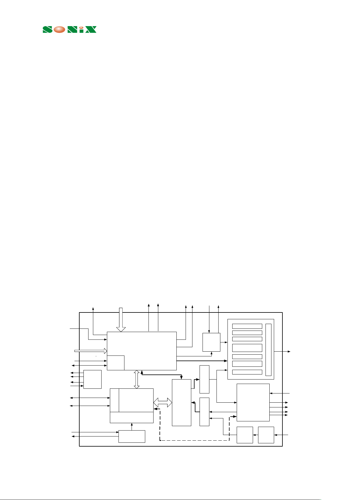
IV. Block diagram
-
CLK
generator
D+
D-
Memory
FIFO
parallel / se r ial
EEPROM
interface
PLL
LEDN
Digital
receiver
S/PDIF OUT
S/PDIF IN
S/PDIF
decoder
serial / par alle l
AC'97 Controller
ACDIN
SCL
SDA
BITC LK
ACRSTN
ACSYNC
ACDOUT
CS
SK
DW
DR
Processor
MCU
interface
VOLUP
VOLDN
MUTEP
MUTER
PDSW
(TYPE0, TYPE1, TYPE2, TYPE3,
PLLEN, RECO RD)
HIDMUTER
M
U
X
User data bi ts
Preamble
Validity
Audio data
Channel status bits
Parity
Aux data
SOF
CMPCLK
XIAUD
XO AUD
USB
DPLL
Transceiver
XIUSB
XO USB
RSTN
SN11113 spec
4
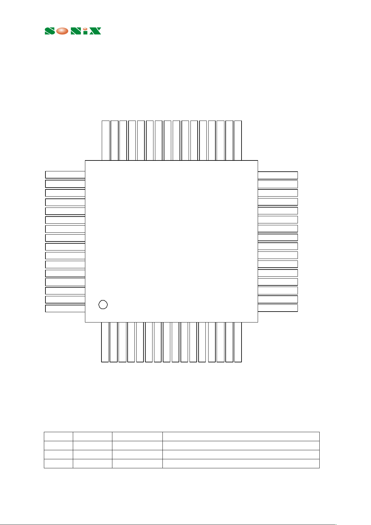
V. Pin description
5.1 SN11113 pin chart (64-pin LQFP)
USB audio controller
SN1 1113
15
10 15
354045
50
55
60
20
25
30
RVDD
TYPE2
SDA
PDSW
SOF
VDDNCVSS
RSTN
TYPE1
NC
NC
RVSS
LEDN
SCL
SPDIFI
SP DI F O
SK
DW
VSS
VDD
XVSS1
XOUSB
DR
XIUSB
CS
RVDD
NC
NC
XIAUD
XOAUD
XVSS2
NC
ACDIN
VDD
XVDD2
VSS
RVSS
RVDD
VOLUP
BITCLK
ACSYNC
RVSS
NC
RECORD
40 35
45
HIDMUTER
MUTEP
PLLEN
AVSS
AVDD
VDD
USBDP
VSS
TAVDD
USBDM
TAVSS
ACDOUT
VOLDN
XVDD1
MUTER
ACRSTN
TYPE 0
CMPCLK
TYPE 3
5.2 pin assignment and description (64-pin LQFP)
Pin No. Pin Name Pin Type Description
1 TYPE1 I, ST Product type setting pin1
2 NC
3 NC
SN11113 spec
5
4 TYPE2 I, ST
Product type setting pin2
5 RSTN I, ST, PU System reset pin, pull low to reset
6 PDSW O, 4mA, SR Power down switch control -- 0: normal mode, 1: power down mode
7 SOF O, 4mA, SR USB SOF (Start of Frame) pin provides 1KHz signal
8 VDD P Power pin
9 VSS P Power pin
10 NC
11 RVDD P Power pin for pad
12 SDA I/O, 4mA, SR IIC data pin for external MCU control
13 SCL I, ST IIC clock pin for external MCU control
14 RVSS P Power pin for pad
15 LEDN O, 8mA, SR LED indicator pin, output low after power on reset, toggle during operation
16 SPDIFI I, ST Input pin for SPDIF signal
17 MUTER I, ST Recording mute, edge trigger with 64ms de-bouncing circuit
18 XVDD1 P Power pin for USB external crystal
19 XIUSB I 6 MHz clock osc pin for USB PLL
20 XOUSB O 6 MHz clock osc pin for USB PLL
21 XVSS1 P Power pin for USB external crystal
22 VDD P Power pin
23 VSS P Power pin
24 DR I, ST EEPROM data input
Fixing this pin to H or L sets USB vendor ID to SONiX USB vendor ID (hex
0C45); PU or PD is used for different product ID
25 DW O, 4mA, SR EEPROM data output
26 SPDIFO O, 8mA, SR SPDIF data output
27 SK O, 4mA, SR EEPROM clock pin
28 RVDD P Power pin for pad
29 CS O, 4mA, SR EEPROM chip select
30 NC
31 NC
32 ACRSTN O, 4mA, SR AC’97 Codec reset
33 RECORD I, ST Recording function enable (=1)
34 NC
35 RVSS P Power pin for pad
36 BITCLK O, 8mA, SR AC’97 serial data clock
37 VOLUP I, ST Volume up control, edge trigger with 64ms de-bouncing circuit
38 ACSYNC O, 4mA, SR AC’97 Codec sync (48 kHz) signal
39 NC
40 ACDIN I, ST AC’97 Codec serial data input
41 VSS P Power pin
42 VDD P Power pin
43 XVSS2 P Power pin for external crystal
44 XOAUD O 12.288 MHz Crystal output
45 XIAUD I, ST 12.288 MHz Crystal input / connected to PLL VCO output
46 XVDD2 P Power pin for external crystal
47 RVSS P Power pin for pad
48 RVDD P Power pin for pad
49 TYPE3 I, ST Product type setting pin3
SN11113 spec
6
50 CMPCLK O, 4mA, SR
PLL comparator input
51 VOLDN I, ST Volume down control, edge trigger with 64ms de-bouncing circui t
52 ACDOUT O, 4mA, SR AC’97 Codec serial data
53 MUTEP I, ST Playback mute control pin, edge trigger with 64ms de-bouncing circuit
54 PLLEN I, ST Use PLL (=1) or Crystal at XIAUD pin
55 VSS P Power pin
56 VDD P Power pin
57 TAVSS P Power pin for USB transceiver
58 USBDM I/O USB data minus
59 USBDP I/O USB data plus
60 TAVDD P Power pin for USB tran sceiver
61 AVSS P Power pin for PLL
62 AVDD P Power pin for PLL
63 HIDMUTER O, 8mA, SR Playback mute led indicator
64 TYPE0 I, ST Product type setting pin0
** All input pin are 5 volt tolerance, TTL level and Schmitt trigger
All output pins are slew rate control
I – input pin , O – output pin, P – power pin, ST – Schmitt trigger, SR – slew rate control,
PU/PD – pull up or pull down
SN11113 spec
7
VI. Operating rating and electrical characteristics
6.1 Absolute maximum rating
symbol Parameter value unit
Dvmin min digital supply voltage DGND – 0.3 V
Dvmax max digital supply voltage DGND + 4.6 V
Avmin min analog supply voltage AGND – 0.3 V
Avmax max analog supply voltage AGND + 4.6 V
Dvinout voltage on any digital input or output
pin
DGND –0.3 to 5.5 V
Avinout voltage on any analog input or output
pin
AGND –0.3 to Avdd + 0.3 V
T
stg
storage temperature range -40 to +125
0
C
ESD (HBM) ESD human body mode
C=100pF, R=1.5KΩ
5000 V
ESD (MM) ESD machine mode 200 V
I
off
Leakage current 10 uA
I
latch
minimum latch up current 100 mA
6.2 Operation conditions
symbol Parameter value unit
DVdd digital supply voltage +3 to +3.6 V
Avdd analog supply voltage +3 to +3.6 V
TA operating ambient temperature range 0 to 70
0
C
TJ operating junction temperature range 0 to 115
0C
6.3 DC electrical characteristics
symbol parameter test condition Value unit
VDI differential input sensitivity
| (D+) – (D-) |
0.2 (min) V
VCM differential common mode range Included VDI
range
0.8 (min)
2.5 (max)
V
VSE single ended receiver threshold 0.8 (min)
2.0 (max)
V
VIH high level input voltage 2.0 (min) V
VIL low level input voltage 0.8 (max) V
VOH high level output voltage I
OH
= -4 mA 2.3 (min) V
VOL low level output voltage IOL= 4 mA 0.5 (max) V
IIL low level input current VI = 0 V RSTN pin : - 50.0 (max)
the other pins : - 3.0 (max)
µA
 Loading...