

SONIX SN11086 Datasheet

SN11086
2003/2/28 ver 0.1
SN11086
Second Generation USB1.1 Flash Memory Controller
Version 0.1
2003/2/28
1 General Description
SN11086 is a high-performance integrated circuit to access the NAND type Flash memory
via the USB 1.1 bus. It provides a flexible and cost efficient single chip solution for external
storage applications such as USB Disk (Flash Disk). With the capability to be pin-to-pin
compatible to SN11085, the current user of SN11085 can easily upgrade to SN11086 with no
engineering effort needed at all. With all the features inherited from SN11085 like the low
6MHz system clock to reduce the EMI, the embedded translation table to eliminate the cost
of external memory, the Sonix proprietary randomization algorithm to extend the lifetime of
flash memory and ensure the product robustness, and the real time ECC correction function,
the SN 11086 adds several other unique features to reduce the cost of the end product and
meet the customer’s requirements.
To enrich the product line of the OEM manufacture, with the ability to support 8 pieces of
flash memories and the new types of 2G bits flashes, SN11086 can be used to build up a
storage device up to 2 Giga bytes. To reduce the total cost of the end product, SN11086
incorporates a power MOS inside to meet the current requirement (500 uA) in USB suspend
state. The usage of EEPROM can also now be eliminated by the capability to program the
customized vendor/product ID/string in the flash itself. Therefore, the total cost is reduced by
upgrade from SN11085 to SN11086.
For fulfilling different customers’ needs, SN11086 now provides several ways to build
different end products. The first one is to provide different security functions. The OEM
manufacturers can program one of the two ways in manufacturing via software. The flashing
ways of LED can also be selected by software now. With these flexibilities, the
manufacturers can easily build different products by using exactly the same components.
1

The USB Mass Storage Class compliance capability of SN11086 makes it a truly
“plug-and-play” device without vendor drivers under Windows 2000/ME/XP and Mac OS
9/10. SN11086 also provides PC boot up and data security function, which makes it an ideal
replacement for the legacy floppy disk.
SN11086
2003/2/28 ver 0.1
2 Features
USB 1.1 12 MHz full-speed compatible
USB 1.1 Mass Storage Class compliant
USB Mass Storage Class Bulk-Only Transport 1.0 supported
USB Mass Storage Class SCSI transparent command set supported
Low system clock (6MHz) to reduce EMI
Customized VID, PID, serial number, and 28 characters of Vendor/Product/Revision
string supported within flash or external EEPROM.
EEPROM in system programmable (ISP) capability
Support Samsung and Toshiba NAND-type flash memory, from 32Mbits to 1Gbits
Support new type of Samsung NAND type flash memory, from 1Gbits to 4Gbits
Real-time ECC correction circuit for data integrity and memory access speed
acceleration
Embedded SRAM for logical-to-physical address translation to extend the life time of
NAND-type flash
Support up to 8 NAND type flash memories are supported
Support up to 2 Gbytes of disk capacity
Embedded FIFO for upstream and downstream data transfer
Built-in power MOS to meet USB suspend requirement (500 uA)
Data transfer rate up to 1.5 MB/s (burst), 1.1 MB/s (read average)
LED indicator pin
Three modes of LED flashing patterns can be selected
PC boot up capability (host BIOS with USB ZIP/HDD boot up support is necessary)
Flash disk security function provided, up to 12 characters of password for high sensitive
data protection from illegally access
Two types of security functions can be selected
ROM-type flash disk capability provided (permanent write protect)
2

SN11086
2003/2/28 ver 0.1
No Driver needed under Microsoft Windows ME/2000/XP, Mac OS 9.x/10.x
Sonix Driver for Microsoft Windows 98
Sonix mass production tool available for mass production
Sonix security program available
Sonix bonus programs available
Single 3.3V operation
48 pin LQFP package
3
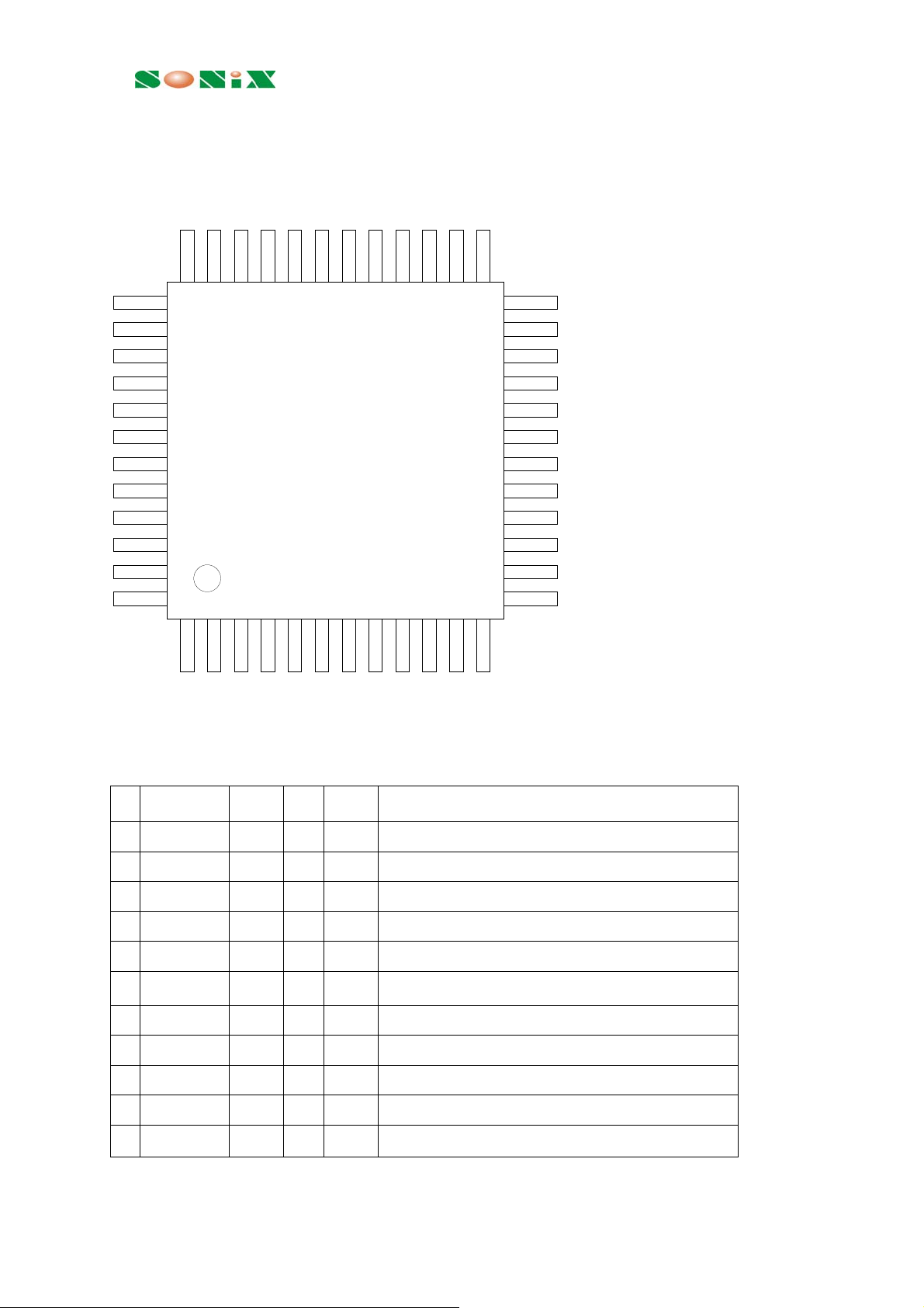
3. Pin Assignment
SN11086
2003/2/28 ver 0.1
DPLUS
DMINUS
FLCE8
FLCE6
FLCE4
FLCE2
AVDD
AVS S
FLD4
FLD5
FLD3
VDD
NC
FLWPS W
35
40
45
15 10
GND
FLD6
ROMDI
ROMDO
FLD2
FLD7
VDD
ROMSK
FLD1
GND
30
FLD0
FLWP
GPIO0
ROMCS
FLRB
FLPOWER
FLRE
FLWE
VDDOUT
FLALE
VDDIN
25
20
15
GND
XOU T
XIN
NC
TES T
RSTN
LED 1
FLCE7
FLCE5
FLCE3
FLCE1
FLCLE
VDD
Table 1 SN11086 pin list (red character is the pins different to SN11085)
# pin name type drive special description
1 GND PWR Digital ground
2 FLD6 DIO 8mA PD Flash memory I/O port bit 6
3 FLD2 DIO 8mA PD Flash memory I/O port bit 2
4 FLD7 DIO 8mA PD Flash memory I/O port bit 7
5 FLD1 DIO 8mA PD Flash memory I/O port bit 1
6 FLD0 DIO 8mA PD Flash memory I/O port bit 0
7 FLWP DO 8mA Flash memory write protect
8 FLRB DI Flash memory ready/busy
9 FLWE DIO 8mA PD Flash memory write enable
10 FLRE DIO 8mA PD Flash memory read enable
11 FLALE DO 8mA Flash memory address latch enable
4
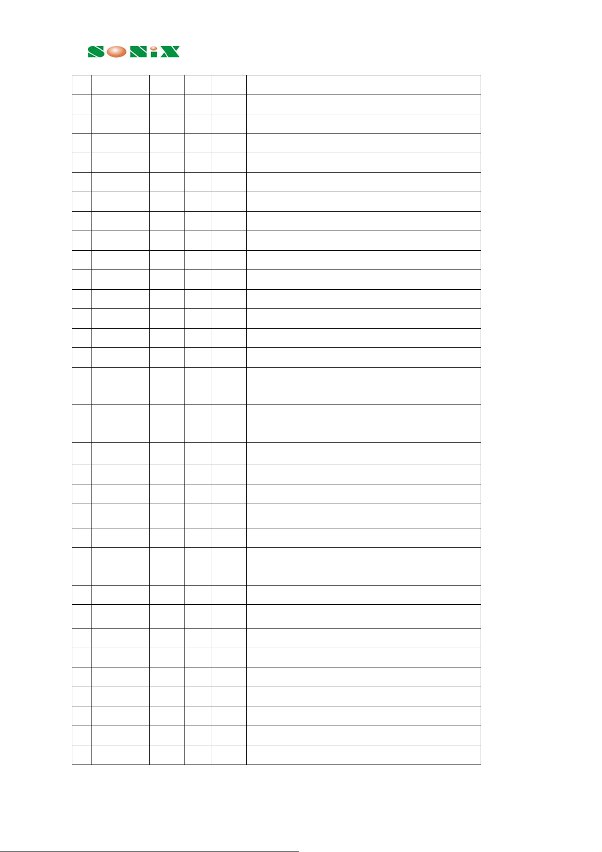
SN11086
2003/2/28 ver 0.1
12 GND PWR Digital ground
13 VDD PWR Digital 3.3V
14 FLCLE DO 8mA Flash memory command latch enable
15 FLCE1 DO 8mA Flash memory chip enable 1
16 FLCE3 DO 8mA Flash memory chip enable 3
17 FLCE5 DO 8mA Flash memory chip enable 5
18 FLCE7 DO 8mA Flash memory chip enable 7
19 LED DIO 8mA PD LED lighter
20 RSTN DI PU Chip reset, connected to external RC circuit
21 TEST DI PD Test pin, NC in normal operation
22 NC - - Do Not Connect
23 XIN I - - Crystal input or oscillator input
24 XOUT O - - Crystal output or no connection
25 VDD PWR - Digital 3.3V
26 FLVDD PWR - 3.3V power to flash VDD
27 FLPOWER DO 8mA OC Flash power control, connect to external MOS
Needs to be pulled up externally.
28 GPIO0 DIO 8mA General Purpose Input/Output for internal test
Always pull up for normal operation
29 ROMCS DO 4mA Chip select for external EEPROM
30 GND PWR Digital ground
31 VDD PWR Digital 3.3V
32 ROMSK DO 4mA Clock for external serial EEPROM
33 ROMDI DO 4mA Serial data to external EEPROM
34 ROMDO DO 4mA Serial data from external EEPROM, pull up
externally if no EEPROM is connected
35 NC - - - DO Not Connect
36 FLWPSW DI PU Flash write protect switch
37 AVDD PWR Analog 3.3V
38 AVSS PWR Analog ground
39 DPLUS AIO - - USB D+ signal
40 DMINUS AIO - - USB D- signal
41 FLCE8 DO 8mA Flash memory chip enable 8
42 FLCE6 DO 8mA Flash memory chip enable 6
43 FLCE4 DO 8mA Flash memory chip enable 4
5
 Loading...