

SONIX SN11085 Datasheet

SN11085
2002/12/01 ver 0.97
SN11085 USB1.1 Flash memory Controller
2002/12/01
ver 0.97
1 General Description
SN11085 is a high-performance integrated circuit to bridge USB 1.1 interface and Flash
memory. It provides a flexible and cost efficient single chip solution for external storage
applications that intend to utilize the convenience of USB. Several special features are
implemented for an efficient and low cost USB storage device solution. The embedded
translation table eliminates external SRAM cost. The Sonix proprietary randomization
algorithm effectively extends the lifetime of flash memory and ensures the product
robustness. Embedded real time ECC correction keeps the data integrity while maintains the
high data transfer rate.
The external serial EEPROM provides customized USB vendor ID, product ID, and string
flexibility. In addition, the EEPROM can contain a serial number which helps the system
manufacturers to track down every single device they made even the design and PID/VID are
all the same. SN11085 also provides in system programming (ISP) capability of the
EEPROM. Products can be assembled without programming the EEPROM in advance,
which saves both the production cost and time. Device and manufacturer’s string can be
saved in the flash instead of the external EEPROM for further total cost reduction.
The USB Mass Storage Class compliance capability of SN11085 makes it a truly
“plug-and-play” device without vendor drivers under Windows 2000/ME/XP and Mac OS
9/10. SN11085 provides PC boot up and data security function, which makes it an ideal
replacement for the legacy floppy disk.
With many of its advanced features and high performance, SN11085 is an ideal choice for
building a portable USB to flash storage system.
1

SN11085
2002/12/01 ver 0.97
2 Features
USB 1.1 full-speed compatible
USB 1.1 Mass Storage Class compliant
USB Mass Storage Class Bulk-Only Transport 1.0 supported
USB Mass Storage Class SCSI transparent command set supported
Customized VID, PID, serial number, and 28 characters of Vendor/Product/Revision
string supported with external EEPROM
EEPROM in system programmable (ISP) capability
28 characters of Vendor/Product/Revision string can be stored in flash for external
EEPROM cost reduction
Support Samsung and Toshiba NAND-type flash memory, from 4Mbytes to 128 Mbytes
Real-time ECC correction circuit for data integrity and memory access speed
acceleration
Embedded SRAM for logical-to-physical address translation of NAND-type flash
Up to 8 NAND type flash memories are supported
Embedded FIFO for upstream and downstream data transfer
Data transfer rate up to 1.5 MB/s (burst), 1.1 MB/s (read average),
LED indicator pin
PC boot up capability (host BIOS with USB ZIP boot up support is necessary)
Flash disk security function provided, up to 12 characters of password for high sensitive
data protection from illegally access
ROM-type flash disk capability provided (permanent write protect)
No Driver needed under Microsoft Windows ME/2000/XP, Mac OS 8.6/9.x/10.x
Sonix Driver for Microsoft Windows 98
Single 3.3V operation
48 pin LQFP package
2
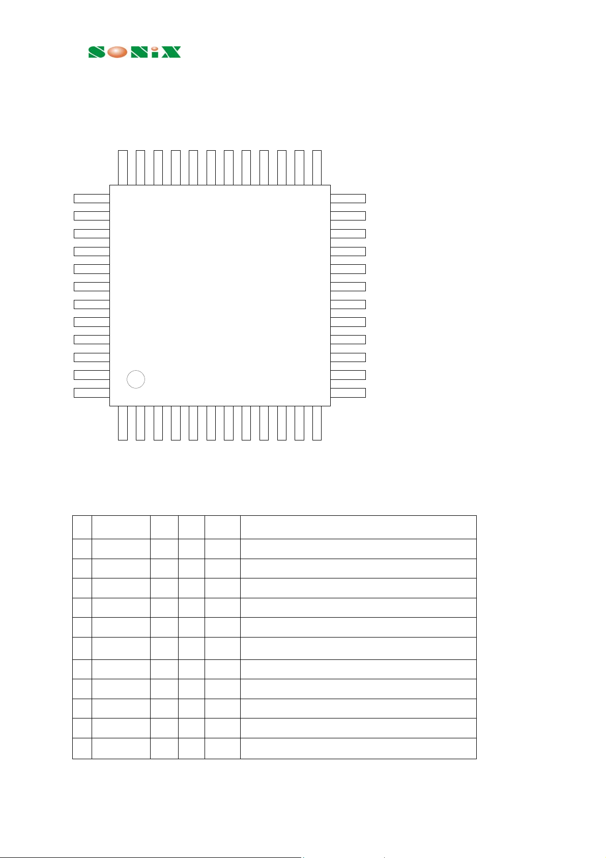
3 Pin Assignment
SN11085
2002/12/01 ver 0.97
AVDD
AVSS
DPLUS
DMINUS
FLCE8
FLCE6
FLCE4
FLCE2
FLD4
FLD5
FLD3
VDD
NC
FLWPSW2
35
40
45
15 10
GND
FLD6
ROMDO
FLD2
ROMDI
FLD7
ROMSK
FLD1
VDD
FLD0
30
GND
FLWP
ROMCS
FLRB
GPIO0
FLWE
NC
FLPOWER
FLRE
FLALE
NC
25
20
15
GND
XOUT
XIN
NC
TEST
RSTN
LED1
FLCE7
FLCE5
FLCE3
FLCE1
FLCLE
VDD
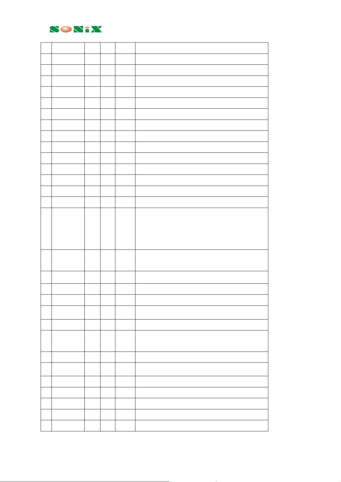
Table 1 SN11085 pin list
# pin name type drive special description
1 GND PWR Digital ground
2 FLD6 DIO 8mA PD Flash memory I/O port bit 6
3 FLD2 DIO 8mA PD Flash memory I/O port bit 2
4 FLD7 DIO 8mA PD Flash memory I/O port bit 7
5 FLD1 DIO 8mA PD Flash memory I/O port bit 1
6 FLD0 DIO 8mA PD Flash memory I/O port bit 0
7 FLWP DO 8mA Flash memory write protect
8 FLRB DI Flash memory ready/busy
9 FLWE DIO 8mA PD Flash memory write enable
10 FLRE DIO 8mA PD Flash memory read enable
11 FLALE DO 8mA Flash memory address latch enable
3
SN11085
2002/12/01 ver 0.97
12 GND PWR Digital ground
13 VDD PWR Digital 3.3V
14 FLCLE DO 8mA Flash memory command latch enable
15 FLCE1 DO 8mA Flash memory chip enable 1
16 FLCE3 DO 8mA Flash memory chip enable 3
17 FLCE5 DO 8mA Flash memory chip enable 5
18 FLCE7 DO 8mA Flash memory chip enable 7
19 LED1 DIO 8mA PD LED1 lighter
20 RSTN DI PU Chip reset, connected to external RC circuit
21 TEST DI PD Test pin, NC in normal operation
22 NC - - No Connect
23 XIN I - - Crystal input or oscillator input
24 XOUT O - - Crystal output or no connection
25 NC - - No Connect
26 NC - - No Connect
27 FLPOWER DO 8mA OC Flash power control
Normal mode – output L
Power down mode – open collector, pull up
externally
28 GPIO0 DIO 8mA General Purpose Input/Output for internal test
Always pull up for normal operation
29 ROMCS DO 4mA Chip select for external EEPROM
30 GND PWR Digital ground
31 VDD PWR Digital 3.3V
32 ROMSK DO 4mA Clock for external serial EEPROM
33 ROMDI DO 4mA Serial data to external EEPROM
34 ROMDO DO 4mA Serial data from external EEPROM, pull up
externally if no EEPROM is connected
35 NC - - - No Connect
36 FLWPSW2 DI PU Flash write protect switch
37 AVDD PWR Analog 3.3V
38 AVSS PWR Analog ground
39 DPLUS AIO - - USB D+ signal
40 DMINUS AIO - - USB D- signal
41 FLCE8 DO 8mA Flash memory chip enable 8
4

SN11085
2002/12/01 ver 0.97
42 FLCE6 DO 8mA Flash memory chip enable 6
43 FLCE4 DO 8mA Flash memory chip enable 4
44 FLCE2 DO 8mA Flash memory chip enable 2
45 FLD4 DIO 8mA PD Flash memory I/O port bit 4
46 FLD5 DIO 8mA PD Flash memory I/O port bit 5
47 FLD3 DIO 8mA PD Flash memory I/O port bit 3
48 VDD P - - Digital 3.3V
Note:
1. P: power pin; AI: analog input pin, AIO: analog input/output pin; DI: digital input pin; DO: digital output pin;
DIO: digital input/output pin.
2. TTL: TTL compatible input pin; PD: pull down; PU: pull up.
3. All pads are Schmitt triggered and with slew rate control
5
 Loading...