

Page 1

1
Eddy DK
Programmer Guide
Ver 2.1.0.3
2009. 10.22
Page 2

2
Revision Date
Document Version
Pages
Description
Feb-5-2009
2.1.0.1
All
Initial release by shlee
Sep-10-2009
2.1.0.2
All
Added WiFi
Oct-14-2009
2.1.0.3
11
J2 pin33 PC12 PC13
J2 pin35 PC13 PC12
Oct-22-2009
2.1.0.3
17,18,19
J2 pin33 PC12 PC13
J2 pin35 PC13 PC12
18,19
J2 pin33 J9_26 J9_33
J2 pin34 J9_25 J9_34
J2 pin33 J9_24 J9_35
Nov-23-2009
2.1.0.3
2,4,6
Added S4M
Revision History
Page 3

3
Table of Contents
Chapter 1. Introduction ................................................................................................................. 5
1.1 About this document ........................................................................................................................ 5
1.2 Who should read this document? .................................................................................................... 5
1.3 Document organization .................................................................................................................... 6
1.4 Eddy-DK Related Documents .......................................................................................................... 7
1.5 Technical Support ............................................................................................................................ 9
Chapter 2. Getting Started ......................................................................................................... 10
2.1 What can you do with Eddy DK ? .................................................................................................. 10
2.2 Eddy-DK Package Contents .......................................................................................................... 10
2.3 Eddy-CPU v2.1 ............................................................................................................................... 11
2.4 Eddy-DK v2.1 ................................................................................................................................. 25
2.5 Eddy-S4M v2.1 ............................................................................................................................... 40
2.6 Eddy-S4M-DK v2.1 ........................................................................................................................ 50
2.7 Eddy-S4M-JiG v2.1 ........................................................................................................................ 59
Chapter 3. Development Environment ........................................................................................ 63
3.1 Source code directory structure .................................................................................................... 63
3.2 Language ........................................................................................................................................ 64
3.3 Development Environment ............................................................................................................. 64
3.4 Installing on Windows OS .............................................................................................................. 64
3.5 Installation of Cygwin ..................................................................................................................... 64
3.6 Configuration of Windows Environment Variables ........................................................................ 67
3.7 Installation of Toolchain ................................................................................................................. 67
3.8 Installation of Eddy DK Source ...................................................................................................... 67
3.9 Installing on Linux ........................................................................................................................... 68
3.10 Installation of Toolchain ................................................................................................................. 68
3.11 Installation of Eddy DK Source ...................................................................................................... 69
3.12 Removing Development Environment ............................................................................................ 69
3.13 Removing Windows Development Environment ............................................................................ 69
3.14 Removing Linux Development Environment .................................................................................. 69
Chapter 4. Compiling of Application Program ............................................................................ 70
4.1 Program Type ................................................................................................................................. 70
4.2 Writing Application Program .......................................................................................................... 72
4.3 Writing Makefile .............................................................................................................................. 72
4.4 Application Program Compile ........................................................................................................ 73
4.5 Compiling on Windows .................................................................................................................. 73
4.6 Compiling on Linux ......................................................................................................................... 73
4.7 Compiling with LemonIDE .............................................................................................................. 74
Page 4

4
4.8 Running Application on Eddy ......................................................................................................... 74
4.9 Uploading and Executing on Eddy ................................................................................................ 74
4.10 Execute a file on Booting of Eddy ................................................................................................. 75
Chapter 5. Creating Firmware .................................................................................................... 76
5.1 How to Create a Firmware ............................................................................................................. 76
5.2 Firmware Upgrade .......................................................................................................................... 78
Chapter 6. Library Introduction ................................................................................................... 81
6.1 Introduction ..................................................................................................................................... 81
6.2 Makefile .......................................................................................................................................... 81
6.3 System functions ............................................................................................................................ 81
6.4 Eddy Environment Function ........................................................................................................... 82
6.5 Serial functions ............................................................................................................................... 84
6.6 Ethernet functions .......................................................................................................................... 87
6.7 GPIO Functions .............................................................................................................................. 92
6.8 ADC Function ................................................................................................................................. 98
6.9 RTC Function .................................................................................................................................. 99
6.10 Debugging Function ....................................................................................................................... 99
Chapter 7. Eddy Software ........................................................................................................ 101
7.1 Software Structure Diagram ......................................................................................................... 101
7.2 Main Applications ......................................................................................................................... 102
7.3 eddy.c Application ........................................................................................................................ 102
7.4 Pinetd.c Application ..................................................................................................................... 102
7.5 Other Applications ........................................................................................................................ 102
Chapter 8. Handling HTML & CGI ............................................................................................ 103
8.1 WEB Configuration ....................................................................................................................... 103
8.2 Example of HTML Code ............................................................................................................... 103
8.3 Example CGI Code ....................................................................................................................... 104
Chapter 9. Appendix ................................................................................................................ 107
9.1 System recovery via Bootloader .................................................................................................. 107
9.2 System recovery via USB............................................................................................................. 112
9.3 Product Specification ................................................................................................................... 118
9.4 Ordering Infomation ...................................................................................................................... 123
Page 5

Chapter 1. Introduction
5
Chapter 1. Introduction
This chapter explains about this manual and introduces the related documents and support.
1.1 About this document
This manual explains about how a programmer can develop a customized application for Eddy module and how this
application can be uploaded and executed on the module. To help programmers with this work, information on
Eddy's operating system and API functions for convenient source writing is supplied.
After reading this document, a programmer can write his or her own application and execute it on the module.
1.2 Who should read this document?
This document is designed for programmers who wish to develop a new application using Eddy DK. It is strongly
recommended that the programmer read this document before starting any programming work. If you are an
administrator or an end user who just needs to apply the module into practical applications, you do not need to read
this document. User's Guide will be helpful in that case. This manual deals with the complete process of writing
source codes and making a firmware that can be uploaded and executed on Eddy module.
Page 6

Chapter 1. Introduction
6
1.3 Document organization
Chapter 1. Introduction is a preface with general information and introductory notices.
Chapter 2. Getting Started gives brief information needed before starting programming work.
Chapter 3. Writing Application explains about the process of writing a customized application and related work..
Chapter 4. Compiling Application deals with the process of compiling your application with Makefile.
Chapter 5. Creating Firmware helps you converting a compiled application into a firmware that can be accepted by
Eddy module.
Chapter 6. Library explains about the library and API functions you can use while programming and application.
Chapter 7. Eddy Software shows how to implement simple TCP/IP and serial routines using example source codes
that are included in the development kit.
Chapter 8. Handling HTML & CGI provides a guide for integrating your own applications with Eddy's web interface.
Chapter 9. Appendix provides programming notes and a list of default utilities.
Page 7

Chapter 1. Introduction
7
Document Name
Description
User Guide
Integration, configuration, and management of Eddy for the
administrator
Programmer’s Guide
Programmer’s application development guide, including in-depth
approach to compiling, linking, and creating firmware
API reference is also included with a list of available functions
for customized application programming
LemonIDE Manual
Guide for primary function of each tool contained in LemonIDE on
Windows and Linux.
Portview User Manual
Guide for SystemBase device server management application
Portview
COM Port Redirector User
Manual
Guide for SystemBase COM Port Redirector
TestView User Manual
Guide for TestView application for testing Eddy serial port and lan
port.
Document Name
Description
Eddy-CPU Spec Sheet
Specifications for Eddy CPU and DK board.
Eddy-S4M Spec Sheet
Eddy-S4M spec description
Eddy-WiFi Spec Sheet
Eddy-WiFi module spec description
LemonIDE Spec Sheet
integrated development environment description
1.4 Eddy-DK Related Documents
The following table summarizes documents included in the Eddy-DK document set.
If you need brief information on Eddy or embedded device servers in general, please visit our corporate website at
http://www.sysbas.com/. You can view and/or download documents related to Eddy as well as latest software and
firmware updates. Available resources are as follows:
Page 8

Chapter 1. Introduction
8
Lemonix Spec Sheet
Lemonix RTOS description
Eddy White Paper
An introductory reading for anyone new to embedded device server.
Deals with background, history, market environment, and technology
All documents are updated promptly, so check for the recent document update. The contents in these documents
are subject to change without any notice in advance.
Page 9

Chapter 1. Introduction
9
1.5 Technical Support
There are three ways you can get a technical support from SystemBase.
First, visit our website http://www.sysbas.com/ and go to ‘Technical Support’ menu. There you can read FAQ
and ask your own question as well.
Second, you can e-mail our technical support team. The mail address is tech@sysbas.com. Any kind of inquiries,
requests, and comments are welcome.
Finally, you can call us at the customer center for immediate support. Our technical support team will kindly help you
get over with the problem.
The number to call is 82-2-855-0501 (Extension number 225). Do not forget to dial the extension number after getting
a welcome message.
Copyright 2007 SystemBase Co., Ltd. All rights reserved.
Homepage: http://www.sysbas.com/
Tel: +82-2-855-0501
Fax: +82-2-855-0580
1601, DaeRyung Post Tower 1, 212-8, Guro-dong, Guro-gu, Seoul, Korea
Page 10

Chapter 2. Getting Started
10
Chapter 2. Getting Started
This chapter explains about packaging and installation, and discusses key features of Eddy-DK.
2.1 What can you do with Eddy DK ?
Eddy DK is designed to help programmers to develop a customized application that can be applied to
Eddy module easier and faster. It has been a time-consuming and burdensome work to port an
operating system and develop an application on a new hardware. Eddy module and Software
Development Kit makes this work easy.
Eddy DK is different with other device servers in which it can run customized applications. Users can
upload most existing socket/serial communication applications that are running on the Linux
environment. This openness allows users to apply wide variety of functions into the module with
relatively less restrictions.
Eddy DK supports IDE (LemonIDE) and SDK environment to help programmers to execute their own
applications on the module. Programmers can easily write applications using the Linux environment,
with the help of SDK and example source codes. Cross-compiler running on the standard Linux
environment helps your applications to run on the Eddy module. Embedded Linux on Eddy can
provide stable and rapid environment for your applications.
2.2 Eddy-DK Package Contents
Eddy-DK includes Eddy module.
Eddy-DK package contains as follows. Make sure following contents are included in the Eddy Serial
DK Package.
- Case of Eddy-DK (Eddy-CPU v2.1 1ea, Eddy-DK v2.1board 1ea)
- Case of Eddy-S4M-DK (Eddy-S4M v2.1 1ea, Eddy-S4M-DK board 1ea, (Option : Eddy-S4M-JIG))
- 1EA , Serial cable
- 1EA , LAN cable
- 1EA, USB A to B Cable
- 1EA , Power adaptor
- 1EA , CD (SystemBase SDK, LemonIDE, compile environment, utilities, manuals)
Page 11
Chapter 2. Getting Started
11
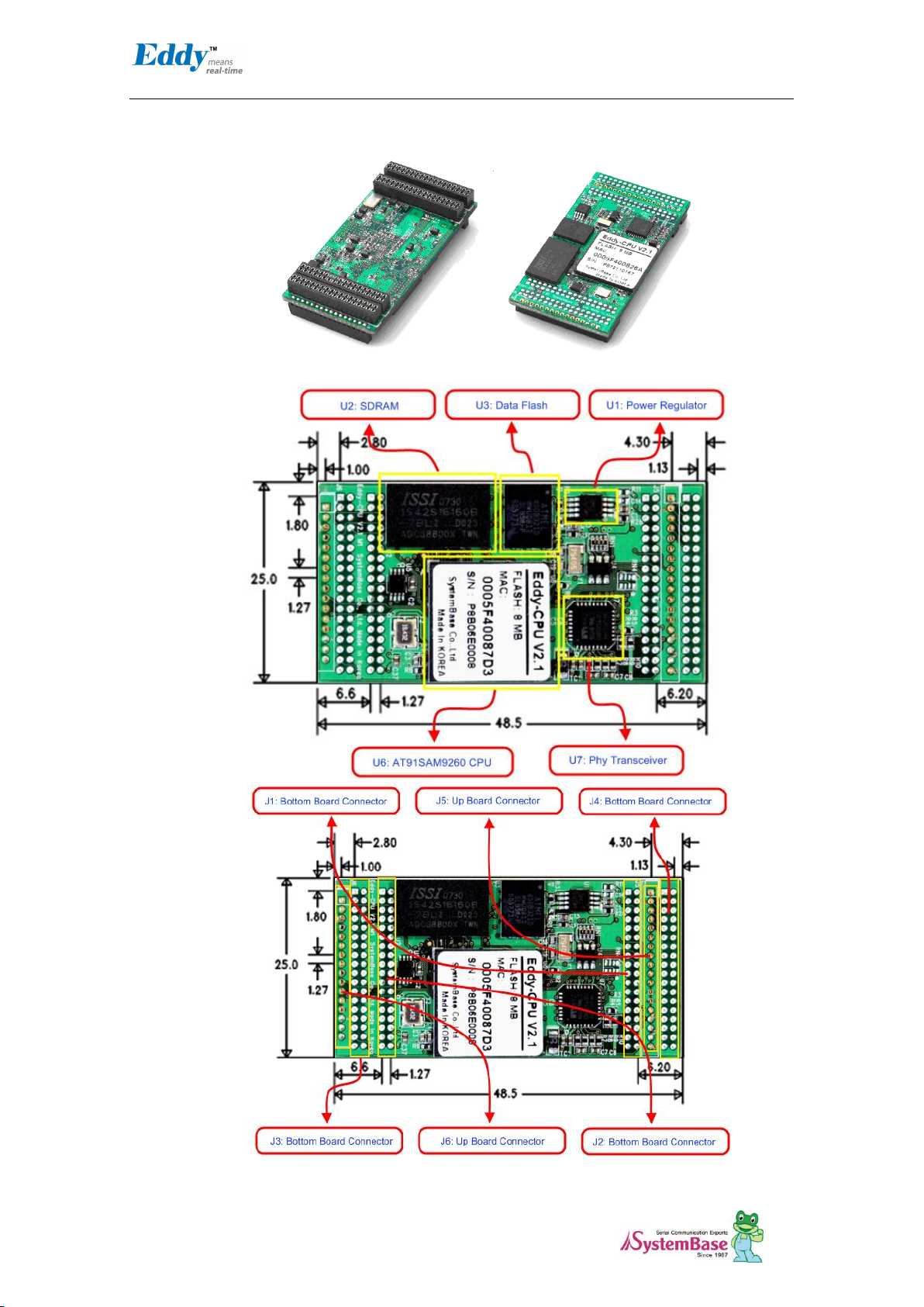
2.3 Eddy-CPU v2.1
Page 12
Chapter 2. Getting Started
12
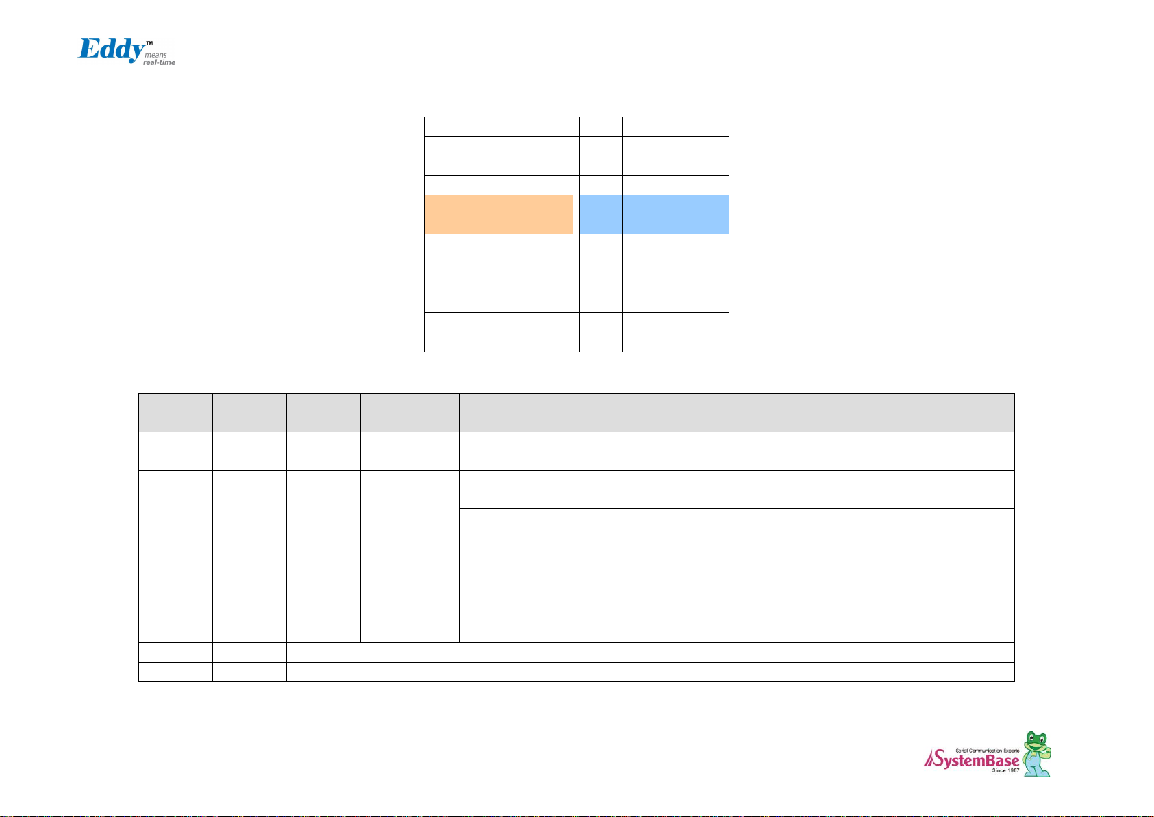
J1 J2
Pin
Signal Name
Pin
Signal Name
Pin
Signal Name
Pin
Signal Name
1
PA5
2 PA4
1 A15
2 A14
3
PC5
4 PC19
3 A13
4 A12 5 PC21
5 PC23
5 A11
5 A10
7
HDMA
8
NC
7 A9
8
A8
9
HDPA
10
DDM
9 A7
10
A6
11
PC26
12
DDP
11
A5
12
A4
13
PC4 (RDY#)
14
PC16
(nRESET)
13
A3
14
A2
15
ICE_NTRST
16
RTCK
15
A1
16
A0
17
TDO
18
TMS
17
PC9
18
NWE
19
TDI
20
TCK
19
FPG
20
NRD
21
3.3V
22
GND
21
GND
22
3.3V
23
3.3V
24
GND
23
GND
24
3.3V
25
PB29 (CTS1)
26
PB28 (RTS1)
25
D7
26
D6
27
PB6 (TXD1)
28
PB7 (RXD1)
27
D5
28
D4
29
A20
30
A19
29
D3
30
D2
31
LAN_Speed
32
LAN_lLink
31
D1
32
D0
33
LAN_RX-
34
LAN_RX+
33
PC13
34
JTAGSEL
35
LAN_TX-
36
LAN_TX+
35
PC12
36
NC
J3 J4
Pin
Signal Name
Pin
Signal Name
Pin
Signal Name
Pin
Signal Name
1
PID0
2 PID1
1 PB12
2 PB13
3
PID2
4 PID3
3 PB30
4 PB31
5
PID4
5 GND
5 PB0
5 PC22
7
PC14
8 PC17
7 PB1
8 PB16
9
PC18
10
PC8 (RTS3)
9 PB2
10
PB17
11
PC20
12
PC10 (CTS3)
11
PB3
12
PB18
13
PA22
14
PC15 (IRQ1)
13
BHDM
14
PB19
15
PB8
16
PB9 (RXD2)
15
BHDP
16
PB20
17
PB10
18
PB11(RXD3)
17
A16
18
PB21
19
PC0
20
PC1 (AD1)
19
A17
20
A18
21
PC2
22
PC3 (AD3)
21
D8
22
D9
23
PB14 (DRXD)
24
PB15 (DTXD)
23
D10
24
D11
25
GND
26
GND
25
D12
26
D13
27
BMS
28
NRST
27
D14
28
D15
29
PB23 / DCD0
30
PB5 / RXD0
29
TWD
30
TCK
31
PB4 / TXD0
32
PB24 / DTR0
31
NANDOE
32
NAND_CLE /
A22
33
PB22 / DSR0
34
PB26 / RTS0
33
NANDWE
34
NAND_ALE /
A21
35
PB27 / CTS0
36
PB25 / RI0
35
NC
36
NC
Eddy-CPU v2.1 Pin Assignment
Page 13
Chapter 2. Getting Started
13
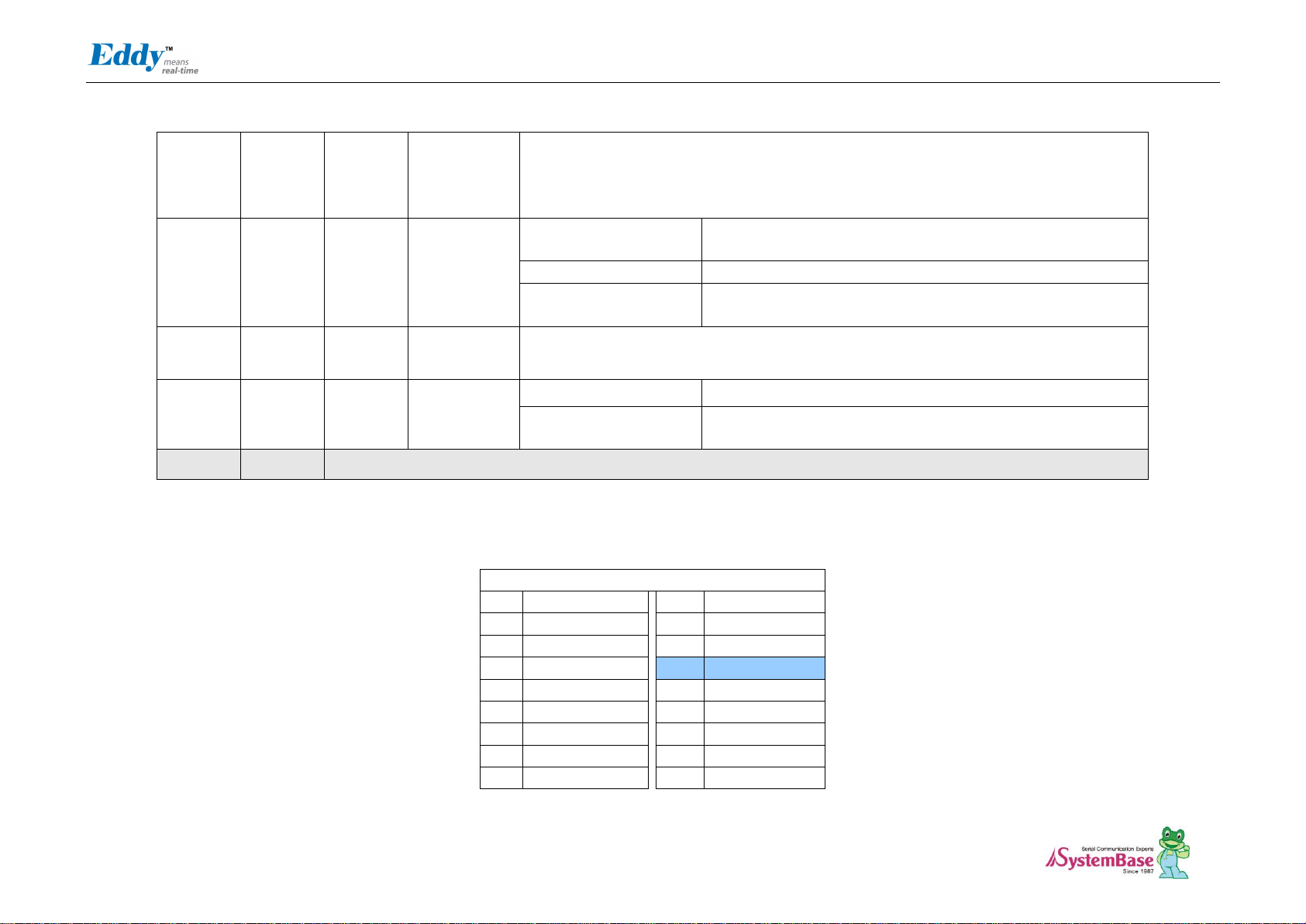
J5
J6
Pin
Signal Name
Pin
Signal Name
1
PB0
2
PB1
1
NC
3
PB2
2
NC
4
PB3
3
3.3V
5
3.3V
4
3.3V
6
3.3V
5 PC25 / BT_Factory
7
BHDM, USB Host Data(-)
6
PB10 / TXD3
8
BHDP, USB Host Data(+)
7
PB11 / RXD3
9
PA31 / TXD4
8
PC8 / RTS3
10
PA30 / RXD4
9
PC10 / CTS3
11
NRST
10
PC24 / BT_MODE
12
GND
11
NRST
13
GND
12
GND
14
PA9 / WPID0
13
GND
15
PC6 / WPID1
14
NC
16
PC7 / WPID2
15
NC
17
NC
16
NC
18
NC
J1
Pin
Signal Name
Pin
Signal Name
1
PA5
2
PA4
3
PC5
4
PC19
5
PC21
5
PC23
7
HDMA
8
NC
9
HDPA
10
DDM
11
PC26
12
DDP
13
PC4 (RDY#)
14
PC16 (nRESET)
15
ICE_NTRST
16
RTCK
17
TDO
18
TMS
19
TDI
20
TCK
21
3.3V
22
GND
23
3.3V
24
GND
25
PB29 (CTS1)
26
PB28 (RTS1)
27
PB6 (TXD1)
28
PB7 (RXD1)
29
A20
30
A19
31
LAN_Speed
32
LAN_lLink
33
LAN_RX-
34
LAN_RX+
35
LAN_TX-
36
LAN_TX+
J1 Specifications
Page 14

Chapter 2. Getting Started
14
Pin No
Name
DK v2.1
Pin No
Expansion
Header Pin No
Description
1
PA5
J10_1
J4_2
Peripheral A : CTS2
UART #2 Clear to Send Signal
Peripheral B : MCBD1
Disabled.
Data Flash connected with SPI0 is used for Eddy-CPU v2.1. For this
reason SPI0 and MCDB0, MCDB3, and MCCDB signals, multiplexing,
cannot be used, thus Multimedia Card Slot B is disabled.
2
PA4
J10_2
J4_1
Peripheral A : RTS2
UART #2 Request to Send Signal
Peripheral B : MCDB2
Disabled.
3
PC5
J10_3
J4_12
Peripheral A : A24
External Address Bus
Peripheral B : SPI1_NPCS1
SPI1(Serial Peripheral Interface) Peripheral Chip Select 1
4
PC19
J10_4
J4_24
Peripheral A : A24
Multimedia Card Slot B Data
Peripheral B : SPI1_NPCS2
SPI1(Serial Peripheral Interface) Peripheral Chip Select 2
5
PC21
J10_5
J4_26
Peripheral A : D21
External Data bus
Peripheral B : EF100
Ethernet(WAN) Force 100Mbit/sec.
6
PC23
J10_6
J4_28
Peripheral A : D23
External Data Bus
7
HDMA
J10_7
J1_27
USB Host Port A Data -
8
NC
J10_8
--
Not Connect
9
HDPA
J10_9
J1_29
USB Host Port A Data +
10
DDM
J10_10
-
USB Device Port Data -
11
PC26
J10_11 - D26
External Data Bus
12
DDP
J10_12
-
USB Device Port Data +
13
PC4
(RDY#)
J10_13
J4_11
Eddy-DK v2,1 : RDY#(OUT)
Ready signal. Output signal for CPU operation status
Peripheral A : A23
External Address Bus
Peripheral B : SPI1_NPCS2
SPI1(Serial Peripheral Interface) Peripheral Chip Select 2
14
PC16
(nRESET)
J10_14
J4_21
Eddy-DK v2,1 : nRESET#(IN)
Polling Input signal continually from External Reset key, implement as
below with checking the constant time of "Low."
Less than 5 seconds: General reset function.
J1 Pin Description
Page 15

Chapter 2. Getting Started
15
More than 5 seconds: Factory Default function.
Peripheral A : D16
External Data Bus
Peripheral B : SPI0_NPCS2
Disabled
SPI0_SPCK, SPI0_MISO, and SPI0_MOSI signals for SPI0 are disabled
as they are not connected externally.
15
ICE_NTRST
J10_15
J7_3
ICE Test Reset Signal
16
RTCK
J10_16
J7_11
Return Test Clock
17
TDO
J10_17
J7_13
Test Data Out
18
TMS
J10_18
J7_7
Test Mode Select
19
TDI
J10_19
J7_5
Test Data In
20
TCK
J10_20
J7_9
Test Clock
21
3.3V
3.0V to 3.6V power input
22
GND
Ground
23
3.3V
3.0V to 3.6V power input
24
GND
Ground
25
PB29
J10_25
J2_30
Peripheral A : CTS1
USART1 Clear To Send
Peripheral B : ISI_VSYNC
Image Sensor Vertical Synchronization
26
PB28
J10_26
J2_29
Peripheral A : RTS1
USART1 Request To Send
Peripheral B : ISI_PCK (IN)
Image Sensor Pixel Clock Provided by the Image Sensor
27
PB6
J10_27
J2_7
Peripheral A : TXD1
USART1 Transmit Data
Peripheral B : TCLK1
Timer Counter ch1 External CLK IN
28
PB7
J10_28
J2_8
Peripheral A : RXD11
USART1 Receive Data
Peripheral B : TCLK2
Timer Counter ch2 External CLK IN
Address Bus
29
A20
J10-29
J1_31
Address Bus
30
A19
J10_30
J1_32
Address Bus
Ethernet 10/100 (Auto MDI/MDIX)
Page 16
Chapter 2. Getting Started
16
31
LED_Speed
J10_31
-
LAN connection speed
Speed
Pin State
LED Definition
10Base-T
H
OFF
100Base-TX
L
ON
32
LED_Link
J10_32
-
LAN connection status
Link/Activity
Pin State
LED Definition
No Link
H
OFF
Link L ON
Activity
Toggle
Blinking
33
LAN_RX-
J10_33 - CPU 내부 Ethernet PHY(WAN)의 Physical receive or transmit signal (- differential)
34
LAN_RX+
J10_34 - CPU 내부 Ethernet PHY(WAN)의 Physical receive or transmit signal (+ differential)
35
LAN_TX-
J10_35 - Physical transmit of CPU Internal Ethernet PHY(WAN) or receive signal (- differential)
36
LAN_TX+
J10_36 - Physical transmit of CPU Internal Ethernet PHY(WAN) or receive signal (+ differential)
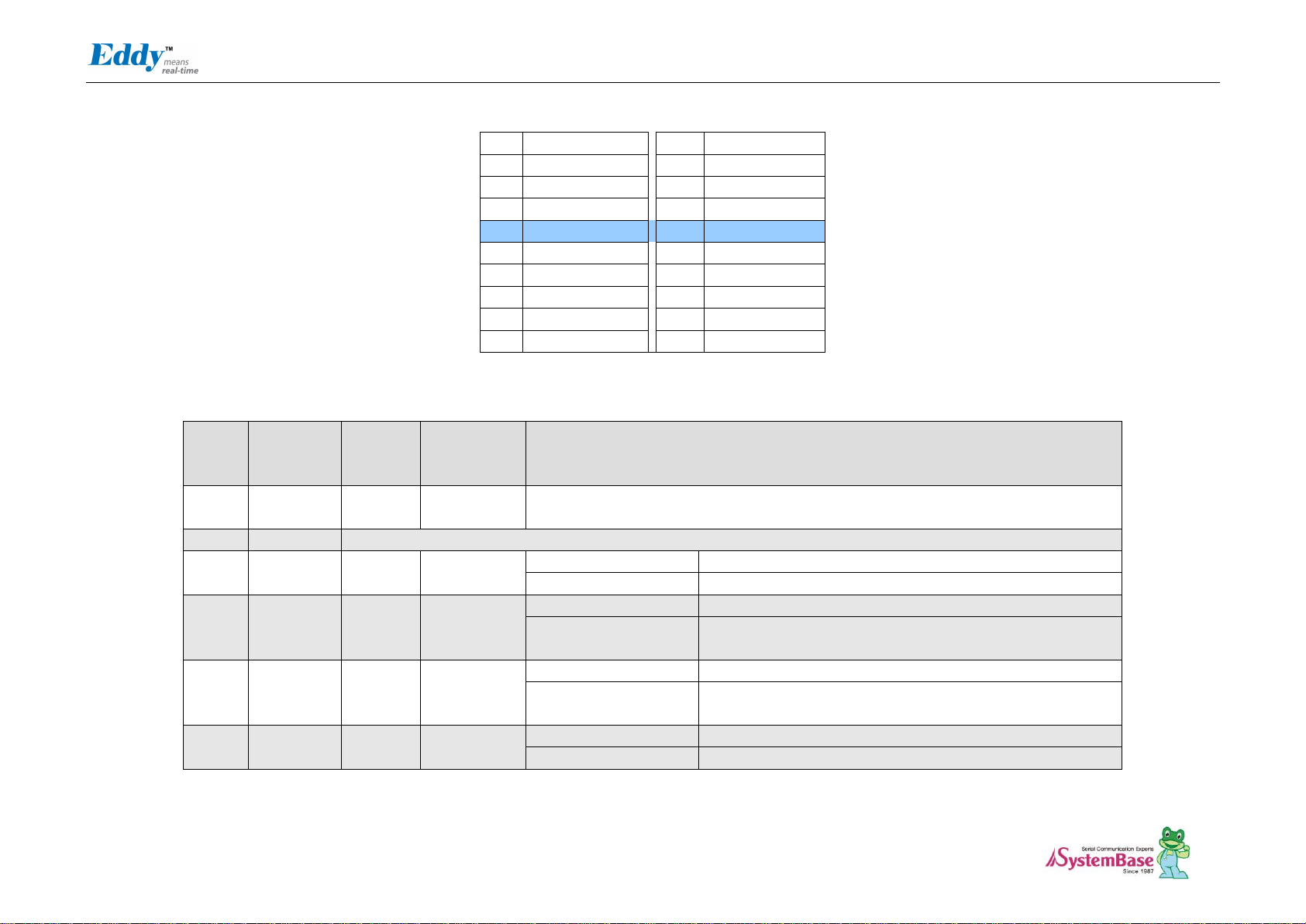
J2
Pin
Signal Name
Pin
Signal Name
1
A15
2
A14
3
A13
4
A12
5
A11
5
A10
7
A9
8
A8
9
A7
10
A6
11
A5
12
A4
J2 Specifications
Connect USB cable to J1 while the jumper is connected to J2, so that applications can be compiled, linked, created, and uploaded to the Eddy-CPU module. (Please refer to
Programmer Guide for more information.)
Page 17
Chapter 2. Getting Started
17
13
A3
14
A2
15
A1
16
A0
17
PC9
18
NWE
19
FPG
20
NRD
21
GND
22
3.3V
23
GND
24
3.3V
25
D7
26
D6
27
D5
28
D4
29
D3
30
D2
31
D1
32
D0
33
PC13
34
JTAGSEL
35
PC12
36
NC
Pin No
Name
DK v2.1
Pin No
Expansion
Header Pin No
Description
1~16
A[15:0]
J9_1
-J9_16
J3_4-J3_20
External Address Bus 0-15 (0 at reset)
DK is directly connected with CPU and external connecter (J3) is connected by buffer.
17
PC9
J9_17
J4_14
Peripheral A : NCS5
External device Chip Select 5.
256MB memory area addressable, active low
Peripheral B : TIOB0
Timer Counter ch0 I/O Line B
18
NEW
J9_18
J1_21
External device Write Enable signal, active low
19
FPG
J9_19
-
For Flash Programming
You can program Data Flash in Eddy CPU v2.1 via USB. Refer to 2.4.2.3 S6:NAND Flash & Data
Flash Chip Select for further information.
20
NRD
J9_20
J1_23
External device Read Enable signal, active low
21, 23
GND
Ground
22, 24
3.3V
3.0V to 3.6V power input
J2 Pin Description
Page 18
Chapter 2. Getting Started
18
25~32
D[7:0]
J9_25
- J3_32
J3_29 - J3_36
External Data Bus 0-7
DK is directly connected with CPU and external connecter (J3) is connected by buffer. You
should enable PC13(NCS6 : Chip Select 6) for working buffer, if you reset, it becomes Pulled-up
input.
33
PC13
J9_33
J4_18
Edd-DK v2.1 : NCS6
Data Bus connected with external header can be used when NCS6
is enabled.
Peripheral A : FIQ
Fast Interrupt Input
Peripheral B : NCS6
External device Chip Select 6
256MB memory area addressable, active low
34
JTAGSEL
J9_34
-
JTAG boundary scan can be used by connecting pin34 and 36(J14 connection). This pin should
not be connected when using ICE (In-Circuit Emulator) or in normal operation status.
35
PC12
J9_35
J4_17
Peripheral A : IRQ0
External Interrupt Input 0
Peripheral B : NCS7
External device Chip Select 7.
256MB memory area addressable, active low
36
NC
Not Connect
J3
Pin
Signal Name
Pin
Signal Name
1
PID0
2
PID1
3
PID2
4
PID3
5
PID4
5
GND
7
PC14
8
PC17
9
PC18
10
PC8 (RTS3)
11
PC20
12
PC10 (CTS3)
13
PA22
14
PC15 (IRQ1)
15
PB8
16
PB9 (RXD2)
J3 Specifications
Page 19
Chapter 2. Getting Started
19
17
PB10
18
PB11(RXD3)
19
PC0
20
PC1 (AD1)
21
PC2
22
PC3 (AD3)
23
PB14 (DRXD)
24
PB15 (DTXD)
25
GND
26
GND
27
BMS
28
NRST
29
PB23 / DCD0
30
PB5 / RXD0
31
PB4 / TXD0
32
PB24 / DTR0
33
PB22 / DSR0
34
PB26 / RTS0
35
PB27 / CTS0
36
PB25 / RI0
Pin No
Name
DK v2.1
Pin No
Expansion
Header Pin
No
Description
1-5
PID[4:0]
J8_1
~J8_5
-
Product ID only used by the manufacturer.
Please do not work on these pins.
6,25,26
GND
Ground
7
PC14
J8_7
J4_19
Peripheral A : NCS3
External Device Chip Select 3
Peripheral B : IRQ2
External Interrupt Input 2
8
PC17
J8_8
J4_22
Peripheral A : D17
External Data Bus
Peripheral B :
SPI0_NPCS3
Disabled
9
PC18
J8_9
J4_23
Peripheral A : D18
External Data Bus
Peripheral B :
SPI1_NPCS1
SPI1(Serial Peripheral Interface) Peripheral Chip Select 1
10
PC8
J8_10
J4_13
Peripheral A : NCS4
External Device Chip Select 4
Peripheral B : RTS3
USART3 Request to Send
J3 Pin Description
Page 20

Chapter 2. Getting Started
20
11
PC20
J8_11
J4_25
Peripheral A : D20
External Data Bus
Peripheral B :
SPI1_NPCS3
SPI1(Serial Peripheral Interface) Peripheral Chip Select 3
12
PC10
J8_12
J4_15
Peripheral A : A25
External Address Bus
Peripheral B : CTS3
USART3 Clear to Send
13
PA22
J8_13
-
Digital I/O Input 4
14
PC15
J8_14
J4_20
Peripheral A : NWAIT
External Wait Signal Input
Peripheral B : IRQ1
External Interrupt Input 2
15
PB8
J8_15
J2_9
Peripheral A : TXD2
UART2 Transmit Data
16
PB9
J8_16
J2_10
Peripheral A : RXD2
UART2 Receive Data
17
PB10
J8_17
J2_11
Peripheral A : TXD3
UART3 Transmit Data
Peripheral B : ISI_D8
Image Sensor Data 8
18
PB11
J8_18
J2_12
Peripheral A : RXD3
UART3 Receive Data
Peripheral B : ISI_D9
Image Sensor Data 9
19
PC0
J8_19
J4_7
Peripheral A : AD0
Analog to Digital Converter Input Ch0
Peripheral B : SCK3
USART3 Serial Clock
20
PC1
J8_20
J4_8
Peripheral A : AD1
Analog to Digital Converter Input Ch1
Peripheral B : PCK0
Programmable Clock Output 0
21
PC2
J8_21
J4_9
Peripheral A : AD2
Analog to Digital Converter Input Ch2
Peripheral B : PCK1
Programmable Clock Output 1
22
PC3
J8_22
J4_10
Peripheral A : AD3
Analog to Digital Converter Input Ch3
Peripheral B :
SPI1_NPCS3
SPI1(Serial Peripheral Interface) Peripheral Chip Select 3
23
PB14
J8_23
J2_15
Peripheral A : DRXD
Debug Receive Data
24
PB15
J8_24
J2_16
Peripheral A : DTXD
Debug Transmit Data
27
BMS
J8_27
-
Boot Mode Select signal
BMS = 1, Boot on Embedded ROM
BMS = 0, Boot on External Memory
28
NRST
J8_28
J1_20
External device Reset signal, active low signal
Page 21

Chapter 2. Getting Started
21
29
PB23
J8_29
J4_28
Peripheral A : DCD0
USART0 Data Carrier Detection
Peripheral B : ISI_D3
Image Sensor Data 3
30
PB5
J8_30
J2_6
Peripheral A : RXD0
USART0 Receive Data
31
PB4
J8_31
J2_5
Peripheral A : TXD0
USART0 Transmit Data
32
PB24
J8_32
J2_25
Peripheral A : DTR0
USART0 Data Terminal Ready
Peripheral B : ISI_D4
Image Sensor Data 4
33
PB22
J8_33
J2_23
Peripheral A : DSR0
USART0 Data Set Ready
Peripheral B : ISI_D2
Image Sensor Data 2
34
PB26
J8_34
J2_27
Peripheral A : RTS0
USART0 Request To Send
Peripheral B : ISI_D6
Image Sensor Data 6
35
PB27
J8_35
J2_28
Peripheral A : CTS0
USART0 Clear To Send
Peripheral B : ISI_D7
Image Sensor Data 7
36
PB25
J8_36
J2_26
Peripheral A : RI0
USART0 Ring Indicator
Peripheral B : ISI_D5
Image Sensor Data 5
Page 22

Chapter 2. Getting Started
22
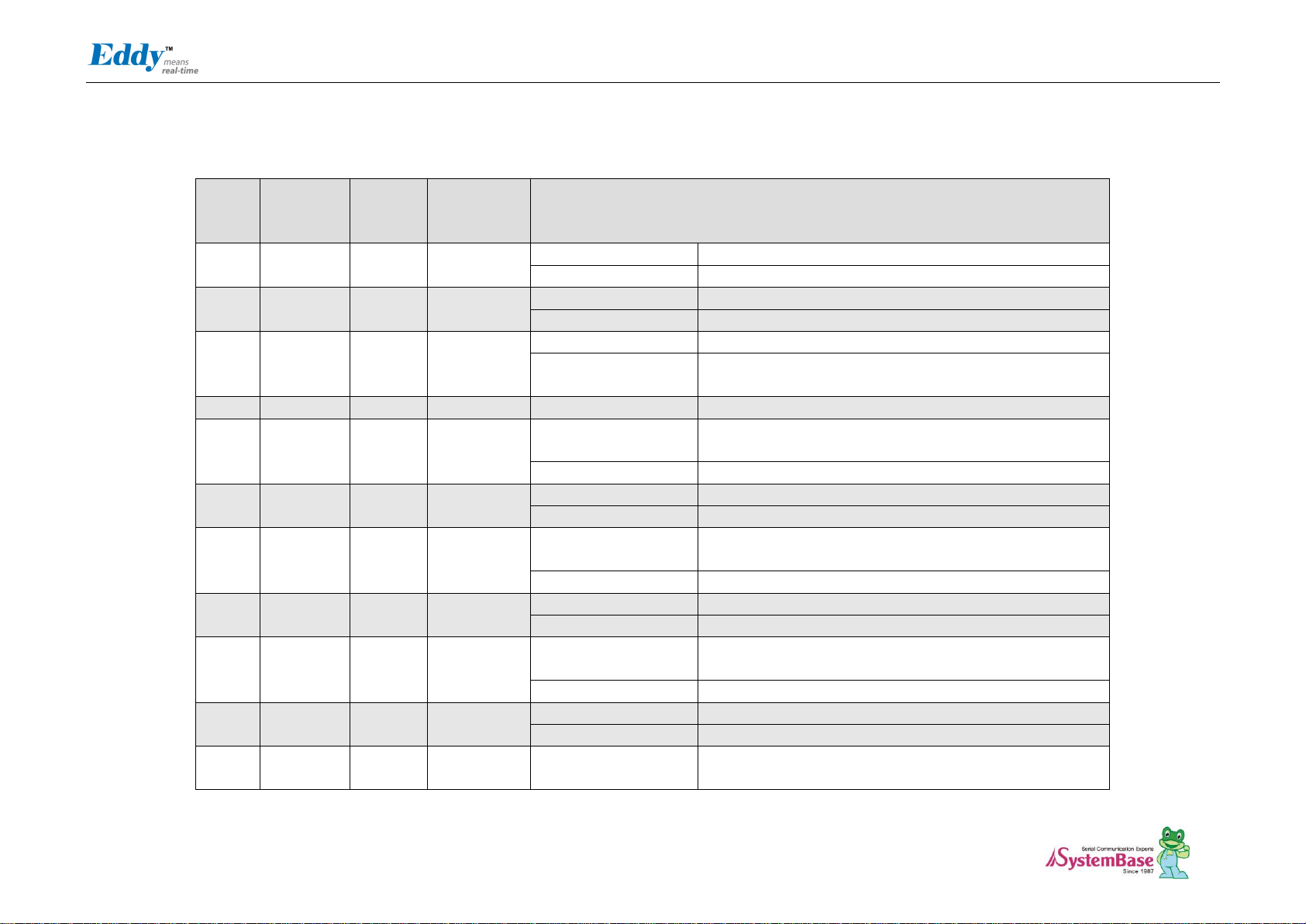
J4
Pin
Signal Name
Pin
Signal Name
1
PB12
2
PB13
3
PB30
4
PB31
5
PB0
5
PC22
7
PB1
8
PB16
9
PB2
10
PB17
11
PB3
12
PB18
13
BHDM
14
PB19
15
BHDP
16
PB20
17
A16
18
PB21
19
A17
20
A18
21
D8
22
D9
23
D10
24
D11
25
D12
26
D13
27
D14
28
D15
29
TWD
30
TCK
31
NANDOE
32
NAND_CLE / A22
33
NANDWE
34
NAND_ALE / A21
35
NC
36
NC
J4 Specifications
Page 23
Chapter 2. Getting Started
23
Pin No
Name
DK v2.1
Pin No
Expansion
Header Pin
No
Description
1
PB12
J11_1
J2_17
Peripheral A : TXD5
USART5 Transmit Data
Peripheral B : ISI_D10
Image Sensor Data 10
2
PB13
J11_2
J2_18
Peripheral A : RXD5
USART5 Receive Data
Peripheral B : ISI_D11
Image Sensor Data 11
3
PB30
J11_3
J2_31
Peripheral A : PCK0
Programmable Clock Output 0
Peripheral B :
ISI_HSYNC
Image Sensor Horizontal Synchronization
4
PB31
J11_4
J2_32
Peripheral A : PCK1
Programmable Clock Output 1
5
PB0
J11_5
J2_2
Peripheral A :
SPI1_MISO
SPI1(Serial Peripheral Interface) Master In Slave Out
Peripheral B : TIOA3
Timer Counter ch3 I/O Line A
6
PC22
J11_6
J4_27
Peripheral A : D22
Peripheral B : TCLK5
Timer Counter ch5 External CLK IN
7
PB1
J11_7
J2_3
Peripheral A :
SPI1_MOSI
Peripheral B : TIOB3
Timer Counter ch3 I/O Line B
8
PB16
J11_8
J2_17
Peripheral A : TK0
SSC Transmit Clock
Peripheral B : TCLK3
Timer Counter ch3 External CLK IN
9
PB2
J11_9
J2_4
Peripheral A :
SPI1_SPCK
SPI1(Serial Peripheral Interface) Serial Clock
Peripheral B : ISI_D3
Image Sensor Data 3
10
PB17
J11_10
J2_18
Peripheral A : TF0
SSC Transmit Frame Sync
Peripheral B : TCLK4
Timer Counter ch4 External CLK IN
11
PB3
J11_11
J2_5
Peripheral A :
SPI1_NPCS0
SPI1(Serial Peripheral Interface) Peripheral Chip Select 0
J4 Pin Description
Page 24
Chapter 2. Getting Started
24
Peripheral B : TIOA5
Timer Counter ch5 I/O Line A
12
PB18
J11_12
J2_19
Peripheral A : TD0
SSC Transmit Data
Peripheral B : TIOB4
Timer Counter ch4 I/O Line B
13
HDMB
J11_13
J1_28
USB Device Port Data -
14
PB19
J11_14
J2_20
Peripheral A : RD0
SSC Receive Data
Peripheral B : TIOB5
Timer Counter ch5 I/O Line B
15
HDPB
J11_15
J1_30
USB Device Port Data +
16
PB20
J11_16
J2_21
Peripheral A : RK0
SSC Receive Clock
Peripheral B : ISI_D0
Image Sensor Data 0
17
A16
J11_17
J3_3
External Address Bus
18
PB21
J11_18
J2_22
Peripheral A : RF0
SSC Receive Frame Sync
Peripheral B : ISI_D1
Image Sensor Data 1
19
A17
J11_19
J3_2
External Address Bus
20
A18
J11_20
J3_1
21-28
D[8:15]
J11_21
~J11_28
J3_28
~J3_21
External Data Bus 8-15
DK is directly connected with CPU and external connecter (J3) is connected by buffer.
PC13(NCS6 : Chip Select 6) should be enabled for working buffer, if it is reset, it work
as Pulled-up input.
29
TWD
J11_29
J4_3
Two-wire Serial Data. This pin cannot be used for GPIO.
30
TWCK
J11_30
J4_4
Two-wire Serial Data. This pin cannot be used for GPIO.
31
NANDOE
J11_31
-
NAND Flash Output Enable
32
A22
J11_32
J1_29
Address Bus
DK is directly connected with CPU and external connecter (J3) is connected by buffer.
33
NANDWE
J11_33
-
NAND Flash Write Enable
34
A21
J11_34
J1_30
Address Bus
35,36
NC
Not Connect
Page 25
Chapter 3. Development
25
NOTE:
Ensure that the input power supply for Eddy Serial DK is from 9V to 48V with 500 mA (or higher).
Environment
2.4 Eddy-DK v2.1
2.4.1 Modules’Locations
2.4.2 Switch Description
Page 26
Chapter 3. Development
26
MODE
Switch
설명
GND
Comm
on
UP
Common GND
COM
(GND)
Isolated Input
Signal(Source)
Eddy DK v2.1
1.1K
4.7K
VCC
Comm
on
Down
Common VCC
EXTERNAL POWER
Isolated Input
Signal(SINK)
Eddy DK v2.1
1.1K
4.7K
ON
1
ON
PIN name
Fuction
Discription
I/O
PC0
ADC0
Temp. Sensor Input(LM50), RN: U22
IN
SW Off : ADC mode
SW ON : GPIO mode
Environment
2.4.2.1. S1~S4: Digital In Select
It is possible to select the Distal Input mode with this switch (S1 ~ S4). In order to use VCC Common
Mode, switch down, and to use GNC Common Mode switch up refer to below feature.
This below schematic is just for reference, So you should make you own schematic with the current
and voltage that you want.
Common Input Setting (Switch S1~S4)
2.4.2.2. S5: ADC Select
You can choice the GPIO and ADC function with this switch. In order to use the ADC device, you
should switch off. And In order to use the GPIO function, you should switch on.
Page 27
Chapter 3. Development
27
PC1
ADC1
Lux. Sensor Input(BH1600), RN: U26
IN
PC2
ADC2
Temp. Sensor Input(TMP300), RN: U24
IN
PC3
ADC3
N/A
IN
ON
ON
1 2
Flash Programming & Booting device Selection
Switch
No 1
Switch
No 2
Operation descriotion
OFF
OFF
For Flash Programming
This setting is needed in firmware Programming. refer to 9.2 System
recovery via USB
OFF
ON
Boot from Data Flash.
ON
OFF
Boot from Nand Flash
ON
ON
Boot from Data Flash or Nand Flash which have bootloader. if Both
devices have the bootloader, algorithm in CPU select the bootloader
of Data Flash.
(Reference : CPU Datasheet 13 장 AT91SAM9260 Boot Program)
ON
ON
1 2 3 4 5 6
Environment
* RN = Reference Number
2.4.2.3. S6: NAND Flash & Data Flash Chip Select
This switch is Nand Flash & Data Flash Chip select switch. This switch is needed in firmware
Programming.
2.4.2.4. S7:UART Select
In order to test Serial Port, UART Select Switches are pulled down. It means that UARTs in CPU are
connected to Serial Port. If switches are pulled up, GPIO Ports are enabled and LEDs are controlled
by GPIO Ports. And if Switch No.6 is pulled up, GPIO ports are connected with the Expansion
Headers.
Page 28
Environment
28
Serial Port & LED
Switch
Bank
Switch
No
Down Position(OFF)
Serial Port Test
UP Position(ON)
GPIO TEST (High : LED On)
S7
1
UART#0 TEST
UART#0 의 TXD, RXD, RTS, CTS
signals are connected with UART#0
RS232 driver IC.
GPIO (PB4, PB5, PB26, PB27) ports are
connected with the GPIO LED of DK
board and disconnected with the
UART#0 RS232 driver IC.
2
UART#0 TEST
UART#0 의 DTR, DSR, DCD, RI signals
are connected with UART#0 RS232
driver IC.
GPIO (PB24, PB22, PB23, PB25) ports
are connected with the GPIO LED of DK
board and disconnected with the
UART#0 RS232 driver IC.
3
UART#1 TEST
UART#1 의 TXD, RXD, RTS, CTS
signals are connected with UART#1
RS232 driver IC.
GPIO (PB6, PB7, PB28, PB29) ports are
connected with the GPIO LED of DK
board and disconnected with the
UART#1 RS232 driver IC.
4
UART#2 TEST
UART#2 의 TXD, RXD, RTS, CTS
signals are connected with UART#2
RS422/485 driver IC.
GPIO (PB8, PB9, PA4, PA5) ports are
connected with the GPIO LED of DK
board and disconnected with the
UART#2 RS422/485 driver IC.
5
UART#3 TEST
UART#3 의 TXD, RXD, RTS, CTS
signals are connected with UART#3
RS422/485 driver IC.
GPIO (PB10, PB11, PC8, PC10) ports
are connected with the GPIO LED of DK
board and disconnected with the
UART#3 RS422/485 driver IC.
6
For Serial Port & GPIO Test
Serial Port and GPIO LED of DK board
are enabled.
Connect to Expansion Header
UART#0~#3 and GPIO LEDs are
disconnected with the Eddy-CPU board
and directly connected with the
Expansion Header(J2, J4)
ON
ON
1 2 3 4
COM PORT#3, #4 settings
Switch
Bank
Switch
No
Down Position(OFF)
UP Position(ON)
S8
Port#3
1
RS485 Half-Duplex mode
RS422 Full-Duplex mode
Chapter 3. Development
2.4.2.5. S8:COM3 & S9: COM4 Select
COM Port #3 and COM Port #4 set the RS422/RS485 mode.
Page 29
Chapter 3. Development
29
2
RS422(RX enabled)
RS485 echo-mode
RS485 non echo-mode
3
RS422 Termination Resistor
not connected
RS422 Termination Resistor
Connected
4
RS485 Termination Resistor
not connected
RS422 Termination Resistor
Connected
S9
Port#4
1
RS485 Half-Duplex mode
RS422 Full-Duplex mode
2
RS422(RX enabled)
RS485 echo-mode
RS485 non echo-mode
3
RS422 Termination Resistor
not connected
RS422 Termination Resistor
Connected
4
RS485 Termination Resistor
not connected
RS422 Termination Resistor
Connected
P10-P17
4x4 Key matrix
I/O
PB20
First Row line
IN
PB21
Second Row line
IN
PB30
Third Row line
IN
PB31
Forth Row line
IN
PC20
First Column line from left
IN
PC21
Second Column line from left
IN
PC22
Third Column line from left
IN
PC23
Fourth Column line from left
IN
Environment
2.4.2.6. SW1~SW16: Key Pad
Key Pad of DK board are consisted with the 4x4 matrix. GPIOs are set to Input mode to read the Key
value. and Key 2, 4, 6, 8 also have the ▲(UP), ▼(DN), ◀(LEFT), ▶(RIGHT) direction function for
LCD menu.
2.4.2.7. SW17: Power
In order to power up, pull up this switch.
Page 30
Chapter 3. Development
30
Pin name
Function
Discription
I/O
PC16
nRESET
Polling Input signal continually from External Reset
key, implement as below with checking the constant
time of "Low."
Less than 5 seconds: General reset function.
More than 5 seconds: Factory Default function.
IN
PIN name
Function
Discription
I/O
PC10
CTS3
UART #3 Clear to Send
I
PC8
RTS3
UART #3 Request to Send
O
PB11
RXD3
UART #3 Receive Data
I
PB10
TXD3
UART #3 Transmit Data
O
Environment
2.4.2.8. Reset1: Reset
2.4.3 LED Description
2.4.3.1. GPIO LED
Eddy-CPU v2.1 supports Max 56 GPIO ports. DK board has 20 GPIO LEDs of all GPIO to test. This
GPIO LEDs are controlled by UART select switches.(refer to 2.4.2.4 UART Select )
Page 31

Environment
31
PA5
CTS2
UART #2 Cleat to Send
I
PA4
RTS2
UART #2 Request to Send
O
PB9
RXD2
UART #2 Receive Data
I
PB8
TXD2
UART #2 Transmit Data
O
PB29
CTS1
UART #1 Cleat to Send
I
PB28
RTS1
UART #1 Request to Send
O
PB7
RXD1
UART #1 Receive Data
I
PB6
TXD1
UART #1 Transmit Data
O
PB25
RI0
UART #0 Ring Indicator
I
PB23
DCD0
UART #0 Data Carrier Detection
I
PB22
DSR
UART #0 Data Set Ready
O
PB24
DTR0
UART #0 Data Terminal Ready
I
PB27
CTS0
UART #0 Clear to Send
I
PB26
RTS0
UART #0 Request to Send
O
PB5
RXD0
UART #0 Receive Data
I
PB4
TXD0
UART #0 Transmit Data
O
Symbol
Parameter
Conditions
Min
Typ
Max
Units
Io
Output Current
PA0-PA31 PB0-PB31
PC0-PC3
16
PC4 - PC31 in 3.3V range
2*
mA
PC4 - PC31 in 1.8V range
4
Chapter 3. Development
41.2 DC Characteristics
* Eddy DK v2.1 has 3.3V range, so PC4-PC31 PIO is set to 2mA.
(Refer to CPU Datasheet의 41.2 DC characteristics )
2.4.3.2. Power, Ready LED
System Ready (RDY): Indicates that the system is operating normally. (Normal: LED blinks)
Power (PWR): Indicates that the 5 V power is being supplied. (Supplying power: Red LED ON)
2.4.3.3. Debug Port LED
DTXD (Debug Port Transmit Dta LED) : Shows transmission status of the Debug Port.
DRXD (Debug Port Receive Data LED) : Shows reception status of the Debug Port.
Page 32

Chapter 3. Development
32
Environment
2.4.3.4. COM Port 1 LED
COM Port 1 Transmit LED : Shows transmission status of COM1 Port.
COM Port 1 Receive LED : Shows reception status of COM1 Port.
2.4.3.5. COM Port 2 LED
COM Port 2 Transmit LED : Shows transmission status of COM2 Port.
COM Port 2 Receive LED : Shows reception status of COM2 Port.
2.4.3.6. COM Port 3 LED
COM Port 3 Transmit LED : Shows transmission status of COM3 Port.
COM Port 3 Receive LED : Shows reception status of COM3 Port.
2.4.3.7. COM Port 4 LED
COM Port 4 Transmit LED : Shows transmission status of COM4 Port.
COM Port 4 Receive LED : Shows reception status of COM4 Port.
2.4.4 External Device Interface Description
Page 33

Environment
33
Pin
Signal
Description
1
TXD+
Transmit Data +
2
TXD-
Transmit Data -
3
RXD+
Receive Data +
6
RXD-
Receive Data -
LED
Description
Left Green
Upon 100BaseT link, it lights
Upon 10BaseT link, it off
Right Yellow
Default Lights, When the data
is sent or received, it blinks.
Chapter 3. Development
2.4.4.1. WAN & LAN Interface
WAN & LAN Port automatically recognizes Cross/ Direct.(auto MDIX)
Page 34

Chapter 3. Development
34
Pin
Signal
Description
1
DCD
Data Carrier Detection (Input) (COM Port 1 only)
2
RXD
Receive Data (Input)
3
TXD
Transmit Data (Output)
4
DTR
Data Terminal Ready (Output) (COM Port 1 only)
5
GND
Ground
6
DSR
Data Set Ready (input) (COM Port 1 only)
7
RTS
Request to Send (Output)
8
CTS
Clear to Send (Input)
9
RI
Ring Indicator (Input)
Pin
Signal
Description
1
TXD+
Transmit differential data positive (Output)
2
TXD-
Transmit differential data negative (Output)
3
GND
Ground 4 RXD+
Receive differential data positive (Input)
5
RXD-
Receive differential data negative (input)
Environment
2.4.4.2. COM Port 1 & COM Port 2
RS232
2.4.4.3. COM Port 3 & COM Port 4
RS422 Full Duplex
Page 35

Chapter 3. Development
35
Pin
Signal
Description
1
TRX+
Transmit/Receive differential data positive
2
TRX-
Transmit/Receive differential data negative
Contact
Polarity
Center (D : 2mm)
9-48VDC
Outer (D: 6.5mm)
Ground
Environment
RS485 Half Duplex
2.4.4.4. Debug Port
You can check debug message or status information with debug port.
Environment Setting
Debug port is configured as follows so user has to set his or her PC serial port connected to debug
port as follows.
Speed: 115200 bps
Data bit: 8 bit
Parity bit: Non Parity
Stop bit: 1 bit
2.4.4.5. Power Jack
Page 36

Chapter 3. Development
36
Signal Name
Function
Description
I/O
P[00:07]
Data bits
Used for data transfer between the CPU and the LCD
module.
I/O
P10
/CS1
Chip enable for D2 (Segment 1 to 64)
IN
P11
/CS2
Chip enable for D3 (Segment 65 to 128)
IN
P12
R/W
R/W signal input is used to select the read /write
mode
High = Read mode, Low = Write mode
IN
P13
D/ I
Register selection input
High = Data register
Low = Instruction register (for write)
Busy flag address counter (for read)
IN
Environment
2.4.5 Internal Device Description
2.4.5.1. EEPROM
Eddy-DK v2.1 has the AT25160, 2Kx8bit SPI EEPROM.
2.4.5.2. LCD Module
Graphic LCD Module (PowerTIP PG12864LRU-JCNH11Q and I2C-Bus I/O Expander IC PCA9539)
Page 37

Chapter 3. Development
37
P14 E Start enable signal to read or write the data.
IN
Function
Description
I/O
P00-P07
DIO Output, Connected with DO[0:7]
OUT
P00
DIO output, DO0
P01
DIO output, DO1
P02
DIO output, DO2
P03
DIO output, DO3
P04
DIO output, DO4
P05
DIO output, DO5
P06
DIO output, DO6
P07
DIO output, DO7
P10-P17
DIO Intput, Connected with DI[0:7]
IN
P10
DIO Input, DI0
P11
DIO Input, DI1
P12
DIO Input, DI2
P13
DIO Input, DI3
P14
DIO Input, DI4
P15
DIO Input, DI5
P16
DIO Input, DI6
P17
DIO Input, DI7
/INT
Connected with PB16 of Eddy-CPU
OUT
Environment
2.4.5.3. 16bit I2C Bus GPIO
This 16-bit I2C Bus GPIO (PCA9539) provides general-purpose remote I/O expansion.
Slave address of this chip is set to 0x74 in DK board. and Address can be changed with A1,A0
address input from 0x74 to 0x77.
16-bit I/O is used to Digital Input/Output as below, and this is connected with the Expansion Header
also. If you use for GPIO, it is possible to configure individually.
2.4.5.4. RTC
- DS1340 (Dallas, I2C interface)
- 12.5pF load capacitance crystal must be used. (Refer to Crystal Spec below)
- Do not use another RTC Chip.
- Backup Battery: CR2032 (235mAh) Lithium Battery.
Page 38

Chapter 3. Development
38
Parameter
Symbol
MIN
TYP
MAX
Units
Normal Frequency
fo
32.768
KHz
Series Resistance
ESR
45,60
KΩ
Load Capacitance
CL
12.5
pF
EddyCPUv2.1
Signal Name
Function
Discription
I/O
A22
CLE
COMMAND LATCH ENABLE
The CLE input controls the activating path for
commands sent to the command register.
OUT
Environment
DS1340 Crystal Specifications
2.4.5.5. Temp Sensor
AD0(PC0)에 National LM50
2.4.5.6. Light Sensor
BH1600FVC (Rohm)
Viout = 0.6 x10⁻⁶ x Ev x R1
Where, Viout = IOUT output voltage [V]
Ev = lilluminance of the ALS(Ambient Light Sensor) surface [lx]
R1 = IOUT output resistor [Ω]
2.4.5.7. NAND Flash
- 256MB, 8bit Flash (Samsung K9F2G08U0A-PCB0)
- Chip Select #3 used, Address range : 0x4000_0000~0x4FFF_FFFF.
The Output voltage is caculated as below
Page 39

Environment
39
A21
ALE
ADDRESS LATCH ENABLE
The ALE input controls the activating path for
address to the internal address registers.
OUT
NANDOE
NANDOE
data-out control
OUT
NANDWE
NANDWE
controls writes to the I/O port
OUT
PC14(NCS3)
NANDCS
device selection control
OUT
PC17
RDYBSY
(R/B)
READY/BUSY OUTPUT
The R/B output indicates the status of the device
operation. When low, it indicates that a program,
erase or random read operation is in process and
returns to high state upon completion. It is an
open drain output and
does not float to high-z condition when the chip
is deselected or when outputs are disabled.
IN
D[0:7]
DATA
bits
DATA INPUTS/OUTPUTS
The I/O pins are used to input command,
address and data, and to output data during read
operations. The I/O pins float to high-z when the
chip is deselected or when the outputs are
disabled.
I/O
Eddy-CPU v2.1
Signal Name
DM9000B
Signal Name
Description
I/O
PC12/NCS7
CSN
Chip Select #7
Address : 0x8000 0000-0x8FFF FFFF
OUT
PC15/IRQ1
INTRN
Interrupt depend on EECK(pin20) setting.
1 : INT pin low active
0 : INT pin high active
EECK is not connected in DK board, so Interrupt is
acted with active high.
IN
A2
CMD
Command Type
When high, Data port
When low, INDEX port
OUT
D[0:15]
Data Bus
16-bit mode
I/O
Chapter 3. Development
2.4.5.8. Ethernet Controller (WAN Port)
- Davicom DM9000B Ethernet Controller
- 16 bit mode set.
- EECS pin should be connected with pull-up resistor to use link/speed LED.
- RJ45 Transformer Center Tap is powered by DM9000B AVDD18.
Page 40

Chapter 3. Development
40
Environment
2.5 Eddy-S4M v2.1
Eddy-S4M is a high-performance mini PCI type embedded module which include ATMEL
AT91SAM9260-CJ porcessor 32MB SDRAM, 8MB DataFlash, 10/100Base-T Ethernet port, Serial 4
Channel, RTC with Battery, minroSD, 4ch ADC, temperature sensor, max 34 programmable GPIO
pins. Eddy-S4M is 59.75 x 61.8mm size. If using Eddy-S4M-JIG board, user could develop their
customized device without other H/W development, which minimizing time and cost to develop.
Referring Example code and Evaluation Kit circuit allow developer to design device they want.
Page 41

Environment
41
Pin
Signal
Pin
Signal
Pin
Signal
Pin
Signal
1
JTAG_TDI
2
JTAG_TDO
63
3.3V
64
PB13
Key Key
65
PB16
66
PB17
2
JTAG_TMS
4
JTAG_RTCK
67
PB18
68
PB19
3
JTAG_TCK
6
ICE_NTRST
69
GND
70
3.3V
7
LAN_RX+
8
LAN_TX+
71
PB20
72
PB21
9
LAN_RX-
10
LAN_TX-
73
PB30
74
GND
11
LAN_Speed
12
LAN_LINK
75
PC0
76
PB31
13
P3_RX-
14
RDY#
77
GND
78
PC1
15
GND
16
NC
79
PC2
80
PC3
17
P3_RX+
18
NC
81
PC5
82
GND
19
3.3V
20
DCD0
83
GND
84
PC9
21
P3_TX+
22
DTR0
85
PC10
86
PC12
Chapter 3. Development
2.5.1 5.1 miniPCI Card Type III Connector Pinout (J5)
Page 42

Environment
42
23
GND
24
3.3V
87
PC13
88
3.3V
25
P3_TX-
26
nRESET
89
3.3V
90
PC14
27
GND
28
3.3V
91
PC15
92
PC17
29
P4_RX+
30
RxD0#
93
PC18
94
PC19
31
3.3V
32
GND
95
PC24
96
PC20
33
P4_RX-
34
RTS0
97
NC
98
PC25
35
P4_TX+
36
TxD0#
99
I2C_TWCK
100
I2C_TWD
37
GND
38
CTS0
101
GND
102
GND
39
P4_TX-
40
3.3V
103
DDM
104
DDP
41
DEBUG_TxD
42
DSR0
105
DM2
106
DP2
43
DEBUG_RxD
44
RI0
107
DM3
108
DP3
45
PA5
46
RxD1#
109
DM4
110
DP4
47
PA22
48
RTS1
111
SDDATA0
112
SDDATA1
49
GND
50
GND
113
SDDATA2
114
GND
51
PA30
52
TxD1#
115
SDCMD
116
SDDATA3
53
NC
54
CTS1
117
SDCDN
118
SDCLK
55
GND
56
NRST
119
JTAG_SEL
120
SDWP
57
PB0
58
PB1
121
NC
122
BMS
59
PB2
60
PB3
123
NC
124
3.3V
61
PB12
62
GND
S4M
Pin No
(124)
Name
S4M-JIG
Pin HDR
(46*2)
S4M-DK
Pin HDR
(46*2)
Description
1
TDI - -
Test Data IN
2
TDO - -
Test Data Out
3
TMS - -
Test Mode Select
4
RTCK - -
Return Test Clock
5
TCK - -
Test Clock
6
NTRST
-
-
Test Reset
119
JTAGSEL
-
-
JTAG boundary scan can be used by connecting J3.
This pin should not be connected when using ICE (In-Circuit
Emulator) or in normal operation status.
S4M
Pin No
(124)
Name
S4M-JIG
Pin HDR
(46*2)
S4M-
DK
Pin
HDR
(46*2)
Description
7
LAN_RX+
J5 pin2
J7 Pn2
Ethernet PHY Physical receive or transmit signal (+ differential) in CPU
8
LAN_TX+
J5 pin1
J7 Pin1
Ethernet PHY Physical receive or transmit signal (- differential) in CPU
9
LAN_RX-
J5 pin3
J7 pin3
Ethernet PHY Physical receive or transmit signal (+ differential) in CPU
Chapter 3. Development
2.5.2 Connector Pinout of Boards
2.5.2.1. ICE and JTAG
2.5.2.2. Ethernet signal from or to PHYceiver
Page 43

Chapter 3. Development
43
10
LAN_TX-
J5 pin4
J7 pin4
Ethernet PHY Physical receive or transmit signal (- differential) in CPU
11
LAN_Speed
J5 pin6
J7 pin6
LAN connection status LED
Link/Activity
Pin State
LED Definition
No Link
H
OFF
Link L ON
Activity
Toggle
Blinking
12
LAN_Link
J5 pin5
J7 pin5
Link/Activity
Pin State
LED Definition
No Link
H
OFF
Link L ON
Activity
Toggle
Blinking
S4M
Pin No
(124)
Name
S4M-JIG
Pin HDR
(46*2)
S4M-DK
Pin HDR
(46*2)
Description
13
P2_RX-
J4 pin20
J6 pin20
COM port #3 Receive differential data negative (Input)
RS422/485 inverting receiver input of Eddy-S4M module
14
RDY#
J4 pin45
J6 pin45
Indicate state of CPU ( normal : blinking)
17
P2_RX+
J4 pin19
J6 pin19
COM port #3 Receive differential data positive (Input)
RS422/485 Noninverting receiver input of Eddy-S4M module
20
DCD0
J4 pin9
J6 pin9
COM port #1 Data Carrier Detection signal
RS232 receiver input of Eddy-S4M module
21
P2_TX+
J4 pin17
J6 pin17
COM port #3 Transmit differential data positive (Output)
RS422/485 Noninverting driver ouput of Eddy-S4M module
22
DTR0
J4 pin7
J6 pin7
COM port #1 Data Terminal Ready signal
RS232 driver output of Eddy-S4M module
25
P2_TX-
J4 pin18
J6 pin18
COM port #3 Transmit differential data negative (Output)
RS422/485 inverting driver ouput of Eddy-S4M module
26
nRESET
J4 pin46
J6 pin46
Reset Input. In S/W, continuously check the interval of ‚LOW‛
when polling input signal from external Reset Key.
Under 5sec : Normal reset function
Over 5sec : Factory Default function
29
P3_RX+
J4 pin23
J6 pin23
COM port #4 Receive differential data negative (Input)
RS422/485 Noninverting receiver input in Eddy-S4M module
30
RxD0#
J4 pin4
J6 pin4
COM port #1 Receive Data signal
RS232 receiver input in Eddy-S4M module
Environment
2.5.2.3. Serial (RS232 & COMBO) and PIOA (Peripheral I/O Controller A)
Page 44

Environment
44
33
P3_RX-
J4 pin24
J6 pin24
COM port #4 Receive differential data negative (Input)
RS422/485 inverting receiver input in Eddy-S4M module
34
RTS0
J4 pin5
J6 pin5
COM port #1 Request To Send signal
RS232 driver output in Eddy-S4M module
35
P3_TX+
J4 pin21
J6 pin21
COM port #4 Transmit differential data positive (Output)
RS422/485 Noninverting driver ouput in Eddy-S4M module
36
TxD0#
J4 pin3
J6 pin3
COM port #1 Transmit Data signal
RS232 driver output in Eddy-S4M module
38
CTS0
J4 pin6
J6 pin6
COM port #1 Request to Send signal
RS232 receiver input in Eddy-S4M module
39
P3_TX-
J4 pin22
J6 pin22
COM port #4 Transmit differential data negative(Output)
RS422/485 inverting driver ouput in Eddy-S4M module
41
DTxD#
J4 pin1
J6 pin1
Transmit Data signal of Debug Port
RS232 driver output in Eddy-S4M module
42
DSR0
J4 pin8
J6 pin8
COM port #1 Data Set Ready signal
RS232 receiver input in Eddy-S4M module
43
DRxD
J4 pin2
J6 pin2
Receive Data signal of Debug Port
RS232 receiver input in Eddy-S4M module
44
RI0
J4 pin8
J6 pin8
COM port #1 Ring Indicator signal
RS232 receiver input in Eddy-S4M module
45
PA5
J5 pin7
J7 pin7
Only used for GPIO
46
RxD1#
J4 pin12
J6 pin12
COM port #1 Receive Data signal
RS232 receiver input in Eddy-S4M module
47
PA22
J5 pin8
J7 pin8
Only used for GPIO
48
RTS1
J4 pin13
J6 pin13
COM port #1 Request to Send signal
RS232 driver output in Eddy-S4M module
51
PA30
J5 pin9
J7 pin9
Only used for GPIO
52
TxD1#
J4 pin11
J6 pin11
COM port #1 Request to Send signal
RS232 driver output in Eddy-S4M module
54
CTS1
J4 pin14
J6 pin14
COM port #1 Request to Send signal
RS232 receiver input in Eddy-S4M module
56
NRST
J5 pin46
J7 pin46
External device Reset output signal (active low)
Chapter 3. Development
Page 45

Chapter 3. Development
45
S4M
Pin No
(124)
Name
S4M-JIG
Pin HDR
(46*2)
S4M-DK
Pin HDR
(46*2)
Description
57
PB0
J5 pin11
J7 pin11
Peripheral A : SPI1_MISO
SPI1(Serial Peripheral Interface)
Master In Slave Out
Peripheral B : TIOA3
Timer Counter ch3 I/O Line A
58
PB1
J5 pin12
J7 pin12
Peripheral A : SPI1_MOSI
SPI1(Serial Peripheral Interface)
Master Out Slave In
Peripheral B : TIOB3
Timer Counter ch3 I/O Line B
59
PB2
J5 pin13
J7 pin13
Peripheral A : SPI1_SPCK
SPI1(Serial Peripheral Interface) Serial
Clock
60
PB3
J5 pin14
J7 pin14
Peripheral A : SPI1_NPCS0
SPI1(Serial Peripheral Interface)
Peripheral Chip Select 0
Peripheral B : TIOA5
Timer Counter ch5 I/O Line A
61
PB12
J5 pin17
J7 pin17
Peripheral A : TXD5
USART5 Transmit Data
64
PB13
J5 pin18
J7 pin18
Peripheral A : RXD5
USART5 Receive Data
65
PB16
J5 pin119
J7 pin119
Peripheral A : TK0
SSC Transmit Clock
Peripheral B : TCLK3
Timer Counter ch3 External CLK IN
66
PB17
J5 pin20
J7 pin20
Peripheral A : TF0
SSC Transmit Frame Sync
Peripheral B : TCLK4
Timer Counter ch4 External CLK IN
67
PB18
J5 pin21
J7 pin21
Peripheral A : TD0
SSC Transmit Data
Peripheral B : TIOB4
Timer Counter ch4 I/O Line B
68
PB19
J5 pin22
J7 pin22
Peripheral A : RD0
SSC Receive Data
Peripheral B : TIOB5
Timer Counter ch5 I/O Line B
71
PB20
J5 pin23
J7 pin23
Peripheral A : RK0
SSC Receive Clock
72
PB21
J5 pin24
J7 pin24
Peripheral A : RF0
SSC Receive Frame Sync
73
PB30
J5 pin25
J7 pin25
Peripheral A : PCK0
Programmable Clock Output 0
75
PC0
J5 pin27
J7 pin27
Peripheral A : AD0
Analog to Digital Converter Input Ch0
76
PB31
J5 pin26
J7 pin26
Peripheral A : PCK1
Programmable Clock Output 1
Environment
2.5.2.4. PIOB and PIOC (Peripheral I/O Controller B/C)
Page 46

Environment
46
78
PC1
J5 pin28
J7 pin28
Peripheral A : AD1
Analog to Digital Converter Input Ch1
Peripheral B : PCK0
Programmable Clock Output 0
79
PC2
J5 pin29
J7 pin29
Peripheral A : AD2
Analog to Digital Converter Input Ch2
Peripheral B : PCK1
Programmable Clock Output 1
80
PC3
J5 pin30
J7 pin30
Peripheral A : AD3
Analog to Digital Converter Input Ch3
Peripheral B : SPI1_NPCS3
SPI1(Serial Peripheral Interface)
Peripheral Chip Select 3
81
PC5
J5 pin33
J7 pin33
Peripheral B : SPI1_NPCS1
SPI1(Serial Peripheral Interface)
Peripheral Chip Select 1
84
PC9
J5 pin34
J7 pin34
Only GPIO
85
PC10
J5 pin35
J7 pin35
Only GPIO
86
PC12
J5 pin36
J7 pin36
Only GPIO
87
PC13
J5 pin37
J7 pin37
Only GPIO
90
PC14
J5 pin38
J7 pin38
Only GPIO
91
PC15
J5 pin39
J7 pin39
Only GPIO
92
PC17
J5 pin40
J7 pin40
Only GPIO
93
PC18
J5 pin41
J7 pin41
Peripheral B : SPI1_NPCS1
SPI1(Serial Peripheral Interface)
Peripheral Chip Select 1
94
PC19
J5 pin42
J7 pin42
Peripheral B : SPI1_NPCS2
SPI1(Serial Peripheral Interface)
Peripheral Chip Select 2
95
PC24
J5 pin44
J7 pin44
Only GPIO
96
PC20
J5 pin43
J7 pin43
Peripheral B : SPI1_NPCS3
SPI1(Serial Peripheral Interface)
Peripheral Chip Select 3
98
PC25
J5 pin45
J7 pin45
Only GPIO
S4M
Pin No
(124)
Name
S4M-JIG
Pin HDR
(46*2)
S4M-DK
Pin HDR
(46*2)
Description
99
I2C_TWCK
J4 pin43
J6 pin43
Two-wire Serial Clock.
This can be used GPIO pin unless RTC function is used.
100
I2C_TWD
J4 pin44
J6 pin44
Two-wire Serial Data. This can be used GPIO pin unless
RTC function is used.
Chapter 3. Development
2.5.2.5. Two Wire Interface
Page 47

Chapter 3. Development
47
S4M
Pin No
(124)
Name
S4M-JIG
Pin HDR
(46*2)
S4M-DK
Pin HDR
(46*2)
Description
103
DDM
J4 pin25
J6 pin25
USB Device Port Data –
104
DDP
J4 pin26
J6 pin26
USB Device Port Data +
105
DM2
J4 pin27
J6 pin27
USB Port2 Data –. Connected to DSPORT2 of GL850A
USB 2.0 Hub Controller.
106
DP2
J4 pin27
J6 pin27
USB Port2 Data +. Connected to DSPORT2 of GL850A
USB 2.0 Hub Controller.
107
DM3
J4 pin29
J6 pin29
USB Port3 Data –. Connected to DSPORT2 of GL850A
USB 2.0 Hub Controller.
108
DP3
J4 pin30
J6 pin30
USB Port3 Data +. Connected to DSPORT2 of GL850A
USB 2.0 Hub Controller.
109
DM4
J4 pin33
J6 pin33
USB Port4 Data -. Connected to DSPORT2 of GL850A
USB 2.0 Hub Controller.
110
DP4
J4 pin34
J6 pin34
USB Port4 Data +. Connected to DSPORT2 of GL850A
USB 2.0 Hub Controller.
S4M
Pin No
(124)
Name
S4M-JIG
Pin HDR
(46*2)
S4M-DK
Pin HDR
(46*2)
Description
111
SDDATA0
J4 pin35
J6 pin35
SD Data0
112
SDDATA1
J4 pin36
J6 pin36
SD Data1
113
SDDATA2
J4 pin37
J6 pin37
SD Data2
115
SDCMD
J4 pin38
J6 pin38
SD command
116
SDDATA3
J4 pin39
J6 pin39
SD Data3
117
SDCDN
J4 pin40
J6 pin40
SD card detect
118
SDCLK
J4 pin41
J6 pin41
SD Clock
120
SDWP
J4 pin42
J6 pin42
SD Write Protect
122
BMS
-
-
Boot Mode Select signal
BMS = 1, Boot on Embedded ROM
BMS = 0, Boot on External Memory
Environment
2.5.2.6. Universal Serial Bus
2.5.2.7. Multimedia Card Interface
Page 48

Environment
48
S4M
Pin No
(124)
Name
S4M-JIG
Pin HDR
(46*2)
S4M-DK
Pin HDR
(46*2)
Description
16, 18, 53,
97,
121, 123
NC
J5 pin10
J5 pin10
No Connection
15, 23, 27,
32, 37, 49,
50, 55, 62,
69, 74, 77,
82, 83, 101,
102, 114
GND
J4: 31,32
J5: 31,32
J6: 31,32
J7: 31,32
Ground
19, 24, 28,
31, 40, 63,
70, 88, 89,
124
3.3V
J4: 15,16
J6: 15,16
3.0 to 3.6V power input
ON
1
ON
Switch No 1
Operation descriotion
OFF
For Flash Programming
Store firmware image to Flash memory through USB Device. (Only
via Window Host). For more information, please refer to chapter 9,
system recovery.
ON
Normal booting via Eddy-S4M v2.1 Data Flash
2.5.2.8. etc
Chapter 3. Development
2.5.3 Switch Operation
2.5.4 LED Operation
System Ready (RDY): Indicate normal state of system (Normal: blinking)
2.5.5 Ethernet
Since there is KSZ8041NL PHY in Eddy-S4M module, when integrating Ethernet, just connect
RJ45 in which transformer located
Page 49

Environment
49
Parameter
Symbol
MIN
TYP
MAX
Units
Normal Frequency
fo 32.768
KHz
Series Resistance
ESR
45,60
KΩ
Load Capacitance
CL 12.5 pF
WARNING : When you use RJ45 which has transformer in its internal circuit, it is possible to
each product doesn’t have equal PIN spec. Therefore, you must confirm PIN number
Bellow is KSZ8041NL functions
• Fully compliant to IEEE 802.3u Standard
• Supports MDI/MDI-X auto crossover (Auto-MDI)
• MII interface support
• RMII interface support with external 50MHz system clock
• ESD rating (6kV)
• Built-in 1.8V regulator for core
• Available in 32-pin (5mm x 5mm) MLF® package
2.5.6 RTC
- We used D1340 which is connected I2C interface.
- In DS1340, you must use crystal of load capacitance = 12.5pF (Refer to bellow Crystal spec)
- You have to confirm Crystal spec because some RTC Chips have different spec
- We used CR2032 (235mAh) Lithium with Backup Battery
DS1340 Crystal Specifications
Chapter 3. Development
2.5.7 Temp Sensor
we used LM50(National) to AD0(PC0)
Page 50

Chapter 3. Development
50
Environment
2.6 Eddy-S4M-DK v2.1
Eddy-S4M DK is Development Kit supporting programmer can easily materialize and test their
application.
2.6.1 Switch and Connector explanation
2.6.1.1. S2 : GPIO Input Configuration
After configure PB0-PB4 to input, you can confirm whether the input value is changing with dip switch
control.
Page 51

Chapter 3. Development
51
Switch No
Down Position(OFF)
UP Position(ON)
1
PB0 Value
Low
High
2
PB0 input value
Low
High
3
PB0 input value
Low
High
4
PB0 input value
Low
High
ON
ON
1 2
Switch No
Down Position(OFF)
UP Position(ON)
1
RS422 Termination Resistor not connected
RS422 Termination Resistor Connected
2
RS485 Termination Resistor not connected
RS422 Termination Resistor Connected
1
RS422 Termination Resistor not connected
RS422 Termination Resistor Connected
2
RS485 Termination Resistor not connected
RS422 Termination Resistor Connected
J6 J7
Pin
Signal
Pin
Signal
Pin
Signal
Pin
Signal
1
DTxD
2
DRxD
1
LAN_RX+
2
LAN_TX+
3
TxD0#
4
RxD0#
3
LAN_RX-
4
LAN_TX-
5
RTS0
6
CTS0
5
LAN_Speed
6
LAN_LINK
7
DTR0
8
DSR0
7
PA5 8 PA22
9
DCD0
10
RI0 9 PA30
10
NC
11
TxD1#
12
RxD1#
11
PB0
12
PB1
13
RTS1
14
CTS1
13
PB2
14
PB3
15
3.3V
16
3.3V
15
5V
16
5V
17
P3_TX+
18
P3_TX-
17
PB12
18
PB13
19
P3_RX+
20
P3_RX-
19
PB16
20
PB17
21
P4_TX+
22
P4_TX-
21
PB18
22
PB19
23
P4_RX+
24
P4_RX-
23
PB20
24
PB21
25
DDM
26
DDP
25
PB30
26
PB31
27
DM2
28
DP2
27
PC0
28
PC1
Environment
2.6.1.2. S3,4 : Terminal Resistor selection
COM Port #3 and COM Port #4 is Combo port which support RS422/RS485 interface. Terminal
resistors in each port are configured by switch upon each Terminal Block.
2.6.1.3. J6,J7 : JIG Board connector(Socket)
Page 52

Chapter 3. Development
52
29
DM3
30
DP3
29
PC2
30
PC3
31
GND
32
GND
31
GND
32
GND
33
DM4
34
DP4
33
PC5
34
PC9
35
SDDATA0
36
SDDATA1
35
PC10
36
PC12
37
SDDATA2
38
SDDATA3
37
PC13
38
PC14
39
SDCMD
40
SDCLK
39
PC15
40
PC17
41
SDCDN
42
SDWP
41
PC18
42
PC19
43
TWCK
44
TWD
43
PC20
44
PC24
45
RDY#
46
nRESET(IN)
45
PC25
46
NRST(OUT)
Environment
2.6.1.4. U7 : Light Sensor
Bellow is comparison between luminance and out current. We used BH1600FVC (Rohm)
The Output voltage is caculated as below
Viout = 0.6 x10⁻⁶ x Ev x R1
Where, Viout = IOUT output voltage [V]
Ev = lilluminance of the ALS(Ambient Light Sensor) surface [lx]
R1 = IOUT output resistor [Ω]
Page 53

Chapter 3. Development
53
Pin Name
Signal Name
Descriotion
Debug Port
TxD
Debug Port Tx LED
RxD
Debug Port Rx LED
COM Port 1
(RS232)
TxD
COM Port1 Tx LED
RxD
COM Port1 Rx LED
COM Port 2
(RS232)
TxD
COM Port2 Tx LED
RxD
COM Port2 Rx LED
COM Port 3
(RS422/RS485)
TxD
If RS422 is COM Port3 Tx LED
If RS485 is Tx/Rx Common LED
Environment
2.6.2 Interface Explanation
2.6.2.1. Power, Ready LED
System Ready (RDY): Indicate normal state of system (Normal: blinking)
Power (PWR): indicate Power is inserted (RED LED ON state)
2.6.2.2. Serial Port LED
Operation description
Page 54

Chapter 3. Development
54
RxD
If RS422 is COM Port3 Rx LED
If RS485 is LED Off (Not Used)
COM Port 4
(RS422/RS485)
TxD
If RS422 is COM Port4 Tx LED
If RS485 is Tx/Rx Common LED
RxD
If RS422 is COM Port4 Rx LED
If RS485 is LED Off (Not Used)
No
Pin Name
Descriotion
I/O 1 PC25
GPIO Only
I/O
2
PC24
GPIO Only
I/O
3
PC20
GPIO or SPI1_NPCS3
I/O 4 PC19
GPIO or SPI1_NPCS2
I/O 5 PC18
GPIO or SPI1_NPCS1
I/O 6 PC17
GPIO Only
I/O
7
PC15
GPIO Only
I/O
8
PC14
GPIO Only
I/O
9
PC13
GPIO Only
I/O
10
PC12
GPIO Only
I/O
11
PC10
GPIO Only
I/O
12
PC9
GPIO Only
I/O
13
PC5
GPIO or SPI1_NPCS1
I/O
14
PC3
GPIO or AD3 or SPI1_NPCS3
I/O
15
PC2
GPIO or AD2 or PCK0
I/O
16
PC1
GPIO or AD1 or PCK0
I/O
17
PC0
GPIO or AD0
I/O
18
PB31
GPIO or PCK1
I/O
19
PB30
GPIO or PCK0
I/O
20
PB21
GPIO or RF0
I/O
21
PB20
GPIO or RK0
I/O
22
PB19
GPIO or RTD0 or TIOB5
I/O
23
PB18
GPIO or TD0 or TIOB4
I/O
24
PB17
GPIO or TF0 or TCLK4
I/O
25
PB16
GPIO or RxD5 or TCLK3
I/O
26
PB13
GPIO or RxD5
I/O
27
PB12
GPIO or TxD5
I/O
28
PB3
GPIO or SPI1_NPCS0 or TIOA5
I/O
29
PB2
GPIO or SPI1_SPCK
I/O
30
PB1
GPIO or SPI1_MOSI or TIOB3
I/O
31
PB0
GPIO or SPI1_MISO or TIOA3
I/O
32
PA30
GPIO Only
I/O
Environment
2.6.2.3. GPIO LED
Eddy-S4M Provide max 34ea GPIO port.
Page 55

Chapter 3. Development
55
33
PA22
GPIO Only
I/O
34
PA5
GPIO Only
I/O
Symbol
Parameter
Conditions
Min
Typ
Max
Units
Io
Output Current
PA0-PA31 PB0-PB31
PC0-PC3
16
PC4 - PC31 in 3.3V range
2*
mA
PC4 - PC31 in 1.8V range
4
Pin
Signal
Description
1
TXD+
Physical transmit or receive signal (+ differential)
2
TXD-
Physical transmit or receive signal (- differential)
3
RXD+
Physical transmit or receive signal (+ differential)
6
RXD-
Physical transmit or receive signal (- differential)
LED
Description
Environment
PIO line has high-drive current capable so that can drive about 16mA except PC4-PC31(2mA).
(41.2 DC characteristics of CPU Datasheet, Refer to bellow)
AT91SAM9260 DC Characteristics
* Since Eddy-S4M v2.1 is 3.3V range, PC4-PC31 PIO can drive 2mA.
2.6.2.4. J10 : Ethernet
Since there is KSZ8041NL PHY in Eddy-S4M module, when integrating Ethernet, just connect
RJ45 in which transformer located
WARNING : When you use RJ45 which has transformer in its internal circuit, it is possible to
each product doesn’t have equal PIN spec. Therefore, you must confirm PIN number
Bellow is KSZ8041NL functions
• Fully compliant to IEEE 802.3u Standard
• Supports MDI/MDI-X auto crossover (Auto-MDI)
• MII interface support
• RMII interface support with external 50MHz system clock
• ESD rating (6kV)
• Built-in 1.8V regulator for core
• Available in 32-pin (5mm x 5mm) MLF® package
Page 56

Chapter 3. Development
56
Left Green
LAN Connection Speed
Speed
Pin
State
LED Definition
10Base-T
H
OFF
100Base-TX
L
ON
Right Yellow
LAN Connection Status
Speed
Pin
State
LED Definition
No Link
H
OFF
Link L ON
Activity
Toggle
Blinking
Pin
Signal
Description
1
DCD
Data Carrier Detection (Input) (COM Port 1 only)
2
RXD
Receive Data (Input)
3
TXD
Transmit Data (Output)
4
DTR
Data Terminal Ready (Output) (COM Port 1 only)
5
GND
Ground 6 DSR
Data Set Ready (input) (COM Port 1 only)
7
RTS
Request to Send (Output)
8
CTS
Clear to Send (Input)
9
RI
Ring Indicator (Input)
Environment
2.6.2.5. J17, 18 : COM Port 1 & Port 2
RS232
* COM Port 2 provide only TxD, RxD, RTS, CTS signal.
Page 57

Chapter 3. Development
57
Pin
Signal
Description
1
TXD+
Transmit differential data positive (Output)
2
TXD-
Transmit differential data negative (Output)
3
GND
Ground 4 RXD+
Receive differential data positive (Input)
5
RXD-
Receive differential data negative (input)
Pin
Signal
Description
1
TRX+
Transmit/Receive differential data positive
2
TRX-
Transmit/Receive differential data negative
Environment
2.6.2.6. J13, 14 : COM Port 3 & Port 4
RS422 Full Duplex
RS485 Half Duplex
J15 : Debug Port
You can confirm debug massage and information of state through debug port.
Environment Configuration
Page 58

Chapter 3. Development
58
Contact
Polarity
Center (D : 2mm)
5VDC
Outer (D: 6.5mm)
Ground
Pin
Signal
Pin
Signal
1
PA5 2 PA22
3
PA30
4
NC 5 PB0 6 PB1
7
PB2 8 PB3
9
PB12
10
PB13
11
PB16
12
PB17
13
PB18
14
PB19
15
3.3V
16
3.3V
17
PB20
18
PB21
19
PB30
20
PB31
21
PC0
22
PC1
23
PC2
24
PC3
25
PC5
26
PC9
Environment
Debug port is configured like below so that you must change serial port (connected with debug port)
configuration like bellow.
- Speed : 115200 bps
- Data bit : 8 bit
- Parity bit : Non Parity
- Stop bit : 1 bit
- Flow control : none
2.6.2.7. S1 : Power Jack
GPIO Connector pinout
Page 59

Chapter 3. Development
59
27
PC10
28
PC12
29
PC13
30
PC14
31
GND
32
GND
33
PC15
34
PC17
35
PC18
36
PC19
37
PC20
38
PC24
39
PC25
40
nRESET(IN)
41
RDY#
42
NRST(OUT)
43
TWCK
44
TWD
Environment
2.7 Eddy-S4M-JiG v2.1
Eddy-S4M JIG board is test board which enable of user to integrate and test their application with
Eddy-S4M. JIG board include mini connector for joining Eddy-S4M, Ethernet RJ45, USB Host, Power,
Reset Switch, and providing connectors to all Eddy-S4M functions.
Page 60

Chapter 3. Development
60
Contact
Polarity
Center (D : 2mm)
5VDC
Outer (D: 6.5mm)
Ground
Pin
Signal
Description
1
TXD+
Physical transmit or receive signal (+ differential)
2
TXD-
Physical transmit or receive signal (- differential)
3
RXD+
Physical transmit or receive signal (+ differential)
6
RXD-
Physical transmit or receive signal (- differential)
LED
Description
Left Green
LAN Connection Speed
Speed
Pin
State
LED Definition
10Base-T
H
OFF
100Base-TX
L
ON
Environment
2.7.1 J6 : Power Jack
2.7.2 J1 : Ethernet
Since there is KSZ8041NL PHY in Eddy-S4M module, when integrating Ethernet, just connect
RJ45 in which transformer located
WARNING : When you use RJ45 which has transformer in its internal circuit, it is possible to
each product doesn’t have equal PIN spec. Therefore, you must confirm PIN number
Bellow is KSZ8041NL functions
• Fully compliant to IEEE 802.3u Standard
• Supports MDI/MDI-X auto crossover (Auto-MDI)
• MII interface support
• RMII interface support with external 50MHz system clock
• ESD rating (6kV)
• Built-in 1.8V regulator for core
• Available in 32-pin (5mm x 5mm) MLF® package
Page 61

Chapter 3. Development
61
Right Yellow
LAN Connection Status
Speed
Pin
State
LED Definition
No Link
H
OFF
Link L ON
Activity
Toggle
Blinking
Pin
Definition
Description
I/O
PC16
nRESET
Polling Input signal continually from External Reset
key, implement as below with checking the constant
time of "Low."
Less than 5 seconds: General reset function.
More than 5 second: Factory Default function.
IN
Environment
2.7.3 J2 : USB Host
J2 is connected to USB HUB ControllerEddy-S4M in Eddy-S4M. Bellow is its PIN spec
2.7.4 RESET switch
Page 62

Chapter 3. Development
62
J4 J5
Pin
Signal
Pin
Signal
Pin
Signal
Pin
Signal
1
DTxD
2
DRxD
1
LAN_RX+
2
LAN_TX+
3
TxD0#
4
RxD0#
3
LAN_RX-
4
LAN_TX-
5
RTS0
6
CTS0
5
LAN_Speed
6
LAN_LINK
7
DTR0
8
DSR0
7
PA5 8 PA22
9
DCD0
10
RI0 9 PA30
10
NC
11
TxD1#
12
RxD1#
11
PB0
12
PB1
13
RTS1
14
CTS1
13
PB2
14
PB3
15
3.3V
16
3.3V
15
5V
16
5V
17
P3_TX+
18
P3_TX-
17
PB12
18
PB13
19
P3_RX+
20
P3_RX-
19
PB16
20
PB17
21
P4_TX+
22
P4_TX-
21
PB18
22
PB19
23
P4_RX+
24
P4_RX-
23
PB20
24
PB21
25
DDM
26
DDP
25
PB30
26
PB31
27
DM2
28
DP2
27
PC0
28
PC1
29
DM3
30
DP3
29
PC2
30
PC3
31
GND
32
GND
31
GND
32
GND
33
DM4
34
DP4
33
PC5
34
PC9
35
SDDATA0
36
SDDATA1
35
PC10
36
PC12
37
SDDATA2
38
SDDATA3
37
PC13
38
PC14
39
SDCMD
40
SDCLK
39
PC15
40
PC17
41
SDCDN
42
SDWP
41
PC18
42
PC19
43
TWCK
44
TWD
43
PC20
44
PC24
45
RDY#
46
nRESET(IN)
45
PC25
46
NRST(OUT)
Environment
2.7.5 J4, 5 : Expansion Header
Provide most function of eddy-S4M with pin connector.
You can confirm the function with direct conjunction to Eddy-S4M-DK.
Page 63

Chapter 3. Development
63
Note
All material related to Eddy including documentation, reference sources and utilities are
periodically updated to www.embeddedmodule.com without prior notice. Please visit and
download latest updates from the site.
Filesystem_2.1.x,
firmware
ramdisk
src
tools
root
Eddy_APPs
Open Source
Busybox
Dropbear
snmp
.
.
vsftpd
include
SB_APIs
web
htdocs
cgi
Environment
Chapter 3. Development Environment
This chapter explains the process of application programming and other important notes.
SDK’s directory structures are as follows.
3.1 Source code directory structure
Firmware Directory
Boot Loader, kernel, filesystem, image are stored.
Ramdisk Directory
Filesystem images are created here
root: Lemonix Filesystem for Filesystem is stored.
Tools Directory
Tools used for creating image files is stored.
Src Directory
Source codes of applicatons in Eddy are stored.
Please refer Chapter4. Compiling Application for the detail description of src directory.
Page 64

Chapter 3. Development
64
Windows
Linux
Windows XP SP2
Windows 2000
Windows 2003
Red Hat 9.0
Fedora Core 4, 5, 6
SUSE Linux Enterprise Server 10.2
Ubuntu Linux 6.x, 7.x
Debian Linuv 4.0
CentOS 4.5
Asianux edition 3
Environment
Eddy-APPs folder contains the source code of the basic application.
Other folders contain open sources for Eddy applications.
3.2 Language
Eddy-DK application should be composed with C language. All example source codes provided are
composed in C language. You can use more than one source file if you are using C programming
Language. If you are familiar with programming with ANSI C, there will be no difficulties creating
applications for Eddy.
3.3 Development Environment
Eddy DK requires Windows or Linux host system.
Officially supported OSs are as follows.
3.4 Installing on Windows OS
This chapter will describe how to install Eddy Development Environment on Windows host.
The explanation of this manual based on Windows XP.
To establish Eddy ’ s integrated development environment, LemonIDE, please refer to
‚LemonIDE_User_Guide‛ for further instructions.
3.5 Installation of Cygwin
To execute LemonIDE on Windows hosts, some of libraries from Linux system are required.
Cygwin is the virtual Linux program which enables Linux environment to be compatible on Windows
hosts. It needs to be installed on the system in order to use LemonIDE.
Run ‚Setup.exe" file from SDK/Windows/Cygwin directory on the CD which is provided with Eddy
DK and follow the instructions below;
Page 65

Environment
65
Select ‚Install from Local Directory‛ and
click ‚Next‛.
Chapter 3. Development
Page 66

Chapter 3. Development
66
Select installation directory as ‚c:\cygwin‛.
Select the folder which Cygwin Package is,
which is
‚SDK\Windows\cygwin‛ on provided DK
CD.
Select the package to install.
Only select ‚Devel‛ as left picture.
Make sure the option changed to ‚Install‛
from ‚Default:.
Environment
Page 67

Chapter 3. Development
67
Environment
3.6 Configuration of Windows Environment Variables
Path should be added in order to refer required Eddy libraries in Windows environment.
Select ‚Desktop‛ ‚My Computer‛ Right click ‚Properties‛ select ‚Advanced‛
tab click ‚Environment Variables‛.
Select Path from System Variable and add the following line on the very beginning.
c:\cygwin\bin;
3.7 Installation of Toolchain
Toolchain compiles source codes composed on Windows environment and make it executable on the
target, Eddy. Eddy. Toolchain installation file, ‚toolchain-windows-arm-411.tgz‛, can be found
under SDK/Windows folder in Eddy DK’s CD. Copy the file to the root directory of ‚C:‛, and
unzip the file from Windows command line as below.
Toolchain should be installed to ‚c:\cygwin\opt\lemonix\cdt‛.
Note that the command is case-sensitive.
3.8 Installation of Eddy DK Source
Install Eddy DK Source. DK Source file, ‚filesystem_2.1.x.x.tar.gz‛, can be found under SDK folder
of Eddy DK’s CD. Copy the file to the root directory of ‚C:‛, and unzip the file from Windows
command line as below.
DK Source should be installed to c:\eddy_DK_2xx‛.
Page 68

Environment
68
Note
Carry out all install procedures under the super user privileges.
Example below assumes that CDROM is mounted on /mnt/cdrom
# cd /
# tar -zxvf /mnt/cdrom/SDK/linux/lemonide*.tar.gz -C /
Note that the command is case sensitive.
Chapter 3. Development
3.9 Installing on Linux
This chapter will describe how to install Eddy Development Environment on Linux host.
The explanation of this manual based on Fedora Core 5.
To establish Eddy ’ s integrated development environment, LemonIDE, please refer to
‚LemonIDE_User_Guide‛ for further instructions.
3.10 Installation of Toolchain
Toolchain compiles source codes composed on Linux environment and make it executable on the
target, Eddy. Toolchain install file, ‚lemonide_linux_10x.tar.gz‛, can be found under SDK/linux
folder in Eddy DK’s CD. Toolchain should be installed to /opt/lemonix.
Note that the command is case sensitive.
If CDROM is mounted on a different location, path displayed below will bear difference.
Page 69

Chapter 3. Development
69
[root@localhost eddy-DK_2xx]# ls -al
Total 32
drwxr-xr-x 6 shlee work 4096 Nov 26 14:43 .
drwxrwxr-- 26 shlee work 4096 Nov 30 21:25 ..
drwxr-xr-x 4 shlee work 4096 Noc 26 14:46 src
-rwxr-xr-x 1 shlee work 2822 Nov 26 14:43 Env.sh
-rwxr-xr-x 1 shlee work 171 Nov 26 14:43 Make.check
drwxr-xr-x 2 shlee work 4096 Nov 29 17:50 firmware
drwxr-xr-x 5 shlee work 4096 Nov 29 17:50 ramdisk
drwxr-xr-x 4 shlee work 4096 Nov 26 14:47 tool
# rm –rf filesystem_2.1.x.x ; Removal of Eddy DK Source
# rm -rf /opt/Lemonix ; Removal of Eddy ToolChain
# pwd
/home/shlee
# tar -zxvf filesystem_2.1.x.x.tar.gz
Environment
3.11 Installation of Eddy DK Source
Install the entire source of Eddy DK. Eddy DK Source file, ‚Filesystem_2.1.x.x.tar.gz‛, can be
found under SDK folder on Eddy DK’s CD.
Install Eddy DK Source as shown below. The eddy_DK_2xx folder will be created after the
installation.
Unzip the file. If Eddy_DK_2xx folder is created, the installation is completed. The below shows the
contents of Eddy_DK_2xx folder.
3.12 Removing Development Environment
Development Environment can be removed by simply deleting the folder where installed files are
located.
3.13 Removing Windows Development Environment
Delete the folders where DK Source and Cywin are installed.
3.14 Removing Linux Development Environment
Page 70

Chapter 4. Compiling of
70
Folder Name
Description
busybox-1.5.0
Linux Utility containing basic commands for the shell
dropbear-0.50
SSH (Secure Shell) Server
gdbserver
Remote debugging program for LemonIDE
(Only executable file provided.)
mtd-util
Management program for Mtd
openssl-0.9.7c
OpenSSL Library (SSL type)
matrixssl-1-8-3
Matrixssl program (SSL type)
thttpd-2.25b
HTTP Server
vsftpd-2.0.5/
FTP Server
ddns-1.8
DDNS Server
ethtool-6
Ethernet based network testing program
netkit-ftp-0.18
ftp client
target-agent
Program helps to upload, download and execute user’s programs,
linked with LemonIDE. The source code not provided.
net-snmp-5.4.1
SNMP V1/V2/V3 program
Iptables-1.3.7
Bridge program for NAT function of LAN port
RT73
WiFi Device Driver
Wireless_tools.29
Wireless support Tool Applications
Application Program
Chapter 4. Compiling of Application Program
4.1 Program Type
This chapter explains how to compose application program, load to Eddy to execute and store it to
flash memory of Eddy as a firmware.
The source codes provided are actual codes containing on the product. Some of codes are not
provided due to a security reason. Program sources can be divided into two categories, Open
Source and Application Source.
Open sources can be found under the ‚scr‛ folder.
The contents are as follows;
Page 71

Chapter 4. Compiling of
71
File name
Description
def.c
Eddy Setting Program
eddy.c
Program which is first executed after booting of Eddy. This program
makes Eddy to operate as configured setting.
pinetd.c
Highest hierarchy of Eddy program; it executes and monitors the
programs of lower hierarchy.
tcp_client.c
Program connects to a server and exchanges data between a serial
port and a socket.
tcp_server.c
Stand ready program exchanges data between the serial port and
the socket.
upgrade.c
Updating Program for Firmware
ddns_agent.c
Program which gives Eddy IP information to DDNS server
detect.c
Program linked with the portview detector.
(Refer the portview manual for the details.)
loopback.c
Loopback test program for the serial port.
portview.c
Agent of Portview, which is a NMS program for windows, provided
by SystemBase.
tcp_broadcast.c
Multi TCP server function supports maximum of five client
connections, and broadcast serial data to all client.
tcp_multiplex.c
Multi TCP server function supports maximum of five client
connections, and transfer serial data to each client.
udp.c
wifi.c
UDP server and client program exchanges data between UDP
socket and a serial port.
WiFi management Program.
rt-test.c
Delay Time Testing Program
testdk.c
Eddy-CPU/S4M Interface Testing program.
test_gpio_led.c
test_gpio_pin.c
GPIO LED Testing Program
GPIO Pin Testing Program
test_adc.c
ADC (Analog Disgital Converter) Testing Program
test_sio.c
Serial Port Testing Program
test_rtc.c
RTC (Real Time Clock) Testing Program
test_dio.c
test_keypad.c
test_nand.c
test_mmc.c
test_lcd.c
test_spi_eeprom.c
DIO (Digital Input Output) Testing Program
Key Pad Testing Program
NAND Flash Testing Program
SD Memory Testing Program
LCD Testing Program
EEPROM Testing Program connected to SPI Interface
/include
Directory for Header files for applications
/SB_APIs
Directory for Exclusive Libraries for Eddy
/web
CGI sources and htm codes for Eddy are located
Application Program
Please refer various source codes under the Eddy_APPs folder when composing new application
programs.
The program sources under the Eddy_APPs folder are the original source codes make Eddy works.
The below is a list of source files located on the Eddy_APPs folder.
Page 72

Chapter 4. Compiling of
72
#include <stdio.h>
int main()
{
While (1)
{
printf("hello world !!!\n");
sleep (1);
}
}
TARGET = eddy pinetd def ddns_agent \
upgrade portview upgradetftp detect \
tcp_server tcp_client tcp_multiplex tcp_broadcast \
udp rt_test hello_world
udp : udp.o
rm -f $@
$(CC) $(CFLAGS) $(LDFLAGS) $(IFLAGS) -o $@ $ $@.o $(LIBS)
$(STRIP) $@
Hello_World : Hello_World.o
Rm -f $@
$(CC) $(CFLAGS) $(LDFLAGS) $(IFLAGS) -o $@ $ $@.o
$(STRIP) $@
Application Program
4.2 Writing Application Program
This chapter shows how to write an application program for Eddy.
First, create a ‚hello_world.c‛ file under the ‚scr/Eddy_APPs‛ directody.
4.3 Writing Makefile
To compile an application program, compile information of the application program has to be
registered on the Eddyy_APPs/Makefile directory. The below is description of ‚Makefile‛ under
directory of src/Eddy_APPs/.
The picture blow shows the environment setting area for an application program compile.
Add a name under the ‚TARGET‛ highlighted as red, and register to the compile environment.
Page 73

Chapter 4. Compiling of
73
C:\eddy_DK_2xx[\src/Eddy_APPs> make hello_world
/opt/lemonix/cdt/bin/arm-linux-gcc -O2 -g -Wall -Wno-nonnull -c -o Hello_World.o Hello_World.c
/opt/lemonix/cdt/bin/arm-linux-gcc -L/opt/lemonix/cdt/lib -L/opt/lemonix/cdt/bin Hello_World.o -o
Hello_World
C:\eddy_DK_2xx[\src/Eddy_APPs>
C:\eddy_DK_2xx[\src/Eddy_APPs> ls
Hello_world SB_APIs def.c eddy kt.c pinetd portview.o
tcp_client.c tcp_client tcp_multiplex.o . . .
[shlee@localhost Eddy_APPs]$make hello_world
/opt/lemonix/cdt/bin/arm-linux-gcc -O2 -g -Wall -Wno-nonnull -c -o hello_world.o hello_world.c
/opt/lemonix/cdt/bin/arm-linux-gcc -L/opt/lemonix/cdt/lib -L/opt/lemonix/cdt/bin hello_world.o
…………
[shlee@localhost Eddy_APPs]$ ls
Hello_World* SB_APIs/ def.c* eddy* kt.c pinetd* portview.o
server* tcp_client* tcp_multiplex.o tcps* upgrade* . . .
Application Program
4.4 Application Program Compile
Compile the application program to execute on Eddy after registering the compile environment to the
‚Makefile‛.
4.5 Compiling on Windows
Enter ‚make‛ command through cmd(command prompt) on the directory where ‚Makefile‛ is
located. As shown below, if a compile is successfully completed, execution file named
‚Hello_World‛ would be created. Of course, as this file was cross-compiled, it can not run on
Windows environment. Upload this file to Eddy using a FTP to execute the file on Eddy, (Files
uploaded with FTPs will not permanently saved on Eddy.).
This will be further explained on the next chapter, Chpater 5 Creating Firmware.
4.6 Compiling on Linux
To compile a source file on Linux environment, enter ‚make‛ command on the directory where
‚Makefile‛ is located. As shown below, if a compile is successfully completed, execution file
named Hello_World would be created. Of course, as this file was cross-compiled, it can not run on
Linux environment. Upload this file to Eddy using a FTP to execute the file on Eddy, (Files uploaded
with FTPs will not permanently saved on Eddy.).
This will be further explained on the next chapter, Chpater 5 Creating Firmware.
Page 74

Chapter 4. Compiling of
74
[shlee@localhost Eddy_APPs]$ ftp 192.168.0.223
Name (192.168.0.223:shlee): eddy
331 Please specify the password.
Password:
230 Login successful.
ftp> cd /tmp
ftp> bin
ftp> put hello_world
8914 bytes sent in 0.00027 seconds (3.3e+04 Kbytes/s)
ftp> bye
[shlee@localhost Eddy_APPs]$
Application Program
4.7 Compiling with LemonIDE
LemonIDE is an IDE(Integrated Development Environment) based on Eclipse platform and provides an
intuitive GUI interface. LemonIDE can be used in both Windows and Linux environments. Source
coding, compile, remote debugging and creating a firmware image can be all carried out with
LemonIDE.
Refer to ‚LemonIDE_User_Guide‛ for detailed information.
4.8 Running Application on Eddy
To run an application on Eddy, there are several methods. First method is to convert an application
as a firmware and loads it into the flash memory area and execute. However, this method is not
recommended for developing phase of application, since it is time consuming task. Second method
is to load and execution file of an application to RAM type file system by using the FTP Server on
Eddy DK, and execute it from there. This method is suitable for developing phase of application;
however the application loaded to Eddy will be deleted when the power is disconnected.
The LemonIDE integrated developing environment provides advanced solution. LemonIDE
debugging tool supports the direct transmission of compiled applications to Eddy. By using this tool,
the user can execute and check the result instantly on site.
If you wish to use LemonIDE, please refer to ‚LemonIDE_User_Guide‛.
4.9 Uploading and Executing on Eddy
Connect to Eddy by using FTP.
ID and password for FTP server are same as the one using with telnet connection.
The example below shows how to upload an example file, ‚hello_world‛, to /tmp folder of Eddy on
Linux using FTP.
When uploading a file, ‚bin‛ command must be entered first for binary mode.
For uploading enter ‚put <file name> on the command line.
On Windows environment, use FTP program of Windows on the Command Prompt.
When the transmission is completed, a user can check the file using Telnet terminal connected Eddy.
The file is executable using ‚chmod‛ command; however the mode has to be switched to
Page 75

Chapter 4. Compiling of
75
# ls
hello_world login.id thttpd.log login.pw
thttpd.pid utmp . . .
#
# chmod 777 hello_world
#
# ./hello_world
Welcome to Eddy !
Welcome to Eddy !
Welcome to Eddy !
Welcome to Eddy !
//<=================================================================
// Here User Application Launching !!
// ----------------------------------------------------------------------------------//
// ex) Task_Launch ("/sbin/hello", argument);
// | |
// | +---- Integer argument
// +--------------- Application name with path
//
//=================================================================>
Task_Launch ("/sbin/hello_world", 0);
signal(SIGCHLD, sig_chld);
Application Program
executable.
After switching to Executable Mode, execute the file by entering ‚/hello_world‛.
To terminate a program, press ‚Ctr‛ and ‚C‛ key simultaneously.
4.10 Execute a file on Booting of Eddy
If auto running is not necessary, you can skip this section.
If the application is successfully executed on Eddy, make a firmware image and load to Flash memory
of Eddy to execute on booting.
Register the application to ‚pinetd.c‛ on the directory of Eddy_APPS.
If ‚printed.c‛ is modified, a user must re-compile it by executing ‚make pinetd‛ as above
example of section 4.4.
Page 76

Chapter 5.
76
(NOTE)
Provided DK Sources are Linux based. Some commands are not executable on Windows
environment. To prevent this problem, a suffix, ‚exe‛, has to be added for some utilities
after file name as shown below.
../tool/genext2fs ../tool/genext2fs.exe
../tool/mkimage ../tool/mkimage.exe
IMAGE=ramdisk
FW_NAME = eddy-fs-2.1.x.x.bin Name and Version Info of Firmware
Image
FIRMWARE_DIR = ../firmware Directory to store created firmware
install:
#@echo "Making ramdisk image..."
#$(TOOL) -b 8192 -d root -D device_table.txt ramdisk
#../tool/genext2fs -U -b 5110 -d root -D device_table.txt ramdisk
#../tool/genext2fs -U -b 7158 -d root -D device_table.txt ramdisk
#../tool/mkcramfs -q -D device_table.txt root ramdisk
./tool/genext2fs.exe -U -b 10240 -N 1024 -d root -D device_table.txt ramdisk Make
size of Ramdisk to 10,240 K and register the device of Eddy/dev as indicated on
Devide_table.txt.
gzip -vf9 ramdisk
est -f ramdisk.gz
./tool/mkimage.exe -A arm -O linux -T ramdisk -C gzip -a 0 -e 0 -n $(FW_NAME) -
d ./ramdisk.gz
$(FW_NAME)
test -f $(FW_NAME)
Creating Firmware
Chapter 5. Creating Firmware
On the previous chapter, we explained how to make and compile application program with sample
program. This chapter introduces methods to create a firmware which permanently saves the
application into the Eddy module and apply it to hardware of Eddy.
5.1 How to Create a Firmware
Firmware image can be created on filesystem_2.1.x.x/ramdisk folder.
Modify ‚Makefile‛ on filesystem_2.1.x.x/ramdisk directory to create a firmware image.
Version info, required Ramdisk amount and desired application to copy can be set up on the
‚Makefile‛.
Page 77

Chapter 5.
77
mv $(FW_NAME) $(FIRMWARE_DIR)/
release: Register the desired application to the directory for copying to
Eddy
cp -f ../src/Eddy_APPs/hello_world root/sbin
cp -f ../src/Eddy_APPs/eddy root/sbin
cp -f ../src/Eddy_APPs/com_redirect root/sbin
cp -f ../src/Eddy_APPs/tcp_server root/sbin
cp -f ../src/Eddy_APPs/tcp_client root/sbin
cp -f ../src/Eddy_APPs/tcp_broadcast root/sbin
cp -f ../src/busybox-1.5.0/busybox root/bin
cp -f ../src/dropbear-0.50/dropbear root/usr/local/sbin
cp -f ../src/dropbear-0.50/dropbearkey root/usr/local/sbin
cp -f ../src/ethtool-6/ethtool root/usr/local/sbin
cp -f ../src/net-snmp-5.4.1/agent/snmpd root/usr/local/sbin
[shlee@localhost ramdisk]$ make release
.
.
[shlee@localhost ramdisk]$ make install
.
.
[shlee@localhost ramdisk]$ ls ../firmware
-rwxr-xr-x -----------------------------------------eddy-bl-2.1.x.x.bin
-rwxr-xr-x -----------------------------------------eddy-bs-2.1.x.x.bin
-rwxr-xr-x -----------------------------------------eddy-os-2.1.x.x.bin
-rwxr-xr-x -----------------------------------------eddy-fs-2.1.x.x.bin
.
.
Creating Firmware
List of task on the ‚Makefile‛ options are as follows;
Make release ; Copy modules registered on the release to Ramdisk area.
Make install ; Create a Filesystem to a firmware image for using on Eddy.
If the modification of ‚Makefile‛ is completed, execute ‚make release and ‚make install‛ in
turns and create a Firmware image.
Created firmware is stored on the ‚FIRMWARE_DIR‛ directory stated on the ‚Makefile‛.
On Windows, use cmd(command prompt) to carry out procedures explained on Linux.
Makefile options are as follows.
Make release ; copy module in release to ramdisk area
Make cfg ; create firmware image of Eddy enviromental files in ramdisk/flash
Make install ; create a firmware image of Eddy’s Filesystem
If changes to Makefile are complete, use ‚make install‛ command to create firmware image.
Page 78

Chapter 5.
78
[shlee@localhost ramdisk]$ make release
.
.
[shlee@localhost ramdisk]$ make install
.
.
[shlee@localhost ramdisk]$ ls ../firmware
-rwxr-xr-x -----------------------------------------eddy-bl-2.1.x.x.bin
-rwxr-xr-x -----------------------------------------eddy-bs-2.1.x.x.bin
-rwxr-xr-x -----------------------------------------eddy-os-2.1.x.x.bin
-rwxr-xr-x -----------------------------------------eddy-fs-2.1.x.x.bin
.
.
FTP
Upload a firmware image using FTP program, and execute the
upgrade command to save it to the Flash memory using Telnet.
Web Browser
Connect to Web server of Eddy and save a firmware to the Flash
memory.
Please refer Eddy_User_Guide for detail information.
Boot Loader
Use the boot loader which operates on booting to save a
firmware through the debugging port of Eddy DK board.
Please refer ‚the chapter 9: System Recovery‛ for detail.
USB
Use USB client port of Eddy DK board to upload a firmware.
Please refer ‚the chapter 9: System Recovery‛ for detail.
Creating Firmware
Firmware will be created in ‚FIRMWARE_DIR‛ directory defined in Makefile.
On Windows, use cmd(command prompt) to carry out procedures explained on Linux.
As shown in the picture above, a new firmware file ‚eddy-fs-2.1.x.x.bin‛ has been created. Now
you have to upload the firmware image to Eddy via Web or FTP, save it to Eddy’s flash memory,
and reset Eddy. Then Eddy will run as the loaded firmware settings.
5.2 Firmware Upgrade
Upload created firmware file to Eddy and save on the Flash Memory.
Eddy provides four ways of upgrading method.
This section explains how to upload a firmware using a FTP.
On Windows, FTP can be used in cmd(command prompt) to carry out upload process.
Upload the created firmware, ‚eddy-fs-2.1.x.x.bin‛, to the /tmp directory of Eddy, using an FTP.
Page 79

Chapter 5.
79
[shlee@localhost firmware]$ ftp 192.168.0.223
Connected to 192.168.0.223.
Name (192.168.0.223:shlee): eddy
331 Please specify the password.
Password:
230 Login successful.
ftp> cd /tmp
250 Directory successfully changed.
ftp> bin
200 Switching to Binary mode.
ftp> put eddy-fs-2.1.x.x.bin
local: eddy-fs-2.1.x.x.bin remote: eddy-fs-2.1.x.x.bin
227 Entering Passive Mode (192,168,0,223,195,50)
150 Ok to send data.
226 File receive OK.
2104287 bytes sent in 0.47 seconds (4.3e+03 Kbytes/s)
ftp> bye
221 Goodbye.
[shlee@localhost firmware]$
# pwd
/tmp
# ls eddy-fs-2.1.x.x.bin
eddy-fs-2.1.x.x.bin
#
# upgrade eddy-fs-2.1.x.x.bin
FileSystem Erase ... 2388341 Bytes
FileSystem Write ... eddy-fs-2.1.x.x.bin, 2388341 Bytes
2388341 (2388341 bytes)
Flash Write OK
Flash Verify OK
…
Creating Firmware
Use Telnet to check ‚eddy-fs-2.1.x.x.bin‛ file is in the /tmp directory.
Use ‚upgrade eddy-fs-2.1.x.x.bin‛ command to update the firmware.
In order for the updated firmware to take effect, you need to reboot the module.
After rebooting you can see the sample program running using Telnet program as shown below.
Page 80

Chapter 5.
80
Eddy login: eddy
Password:
# cd /sbin
# ls
hello_world ifconfig nameif switch_root
com_redirect ifdown pinetd sysctl
…
# ps -ef
PID USER COMMAND
1 root init
2 root [posix_cpu_timer]
3 root [softirq-high/0]
.
.
xx root /sbin/hello_world 1
Welcome to Eddy !
Welcome to Eddy !
Welcome to Eddy !
Welcome to Eddy !
Welcome to Eddy !
Welcome to Eddy !
Welcome to Eddy !
Creating Firmware
Execution result of application program only output to the console port of Eddy. The console is a
debug port of Eddy DK board and only execution result of application program is generated.
The result can be seen on a computer screen using a serial emulator program such as hyper-terminal
on Windows by connecting the debug port to PC and setting communication speed to 115K, None, 8,
1.
Page 81

Chapter 6. Library
81
SB_SetPriority
Function
Specifies priority level of task.
Format
Void SB_SetPriority (int Priority_Level);
Parameter
Priority_level Low (1) ~ High (99)
Returns
None
Notice
Configures the priority level of task execution to the system.
The lowest level is 1, whereas the highest level is 99.
It is recommended to set level below 50; and when a certain task’s level
is set above 50, that task will be executed prior to others, possibly
affecting other tasks’ operation.
SB_GetTick
Introduction
Chapter 6. Library Introduction
This chapter introduces useful libraries and API functions that are applicable with Eddy-Serial DK.
6.1 Introduction
All the functions introduced in this chapter are all APIs included in SB_APIs.a of
/src/Eddy_APPs/SB_APIs directory. You also need to mention this library in the Makefile. All sample
source codes accompanied with Eddy-DK use this library, and you can see the source codes and
Makefile for more information.
6.2 Makefile
Library is in /src/Eddy_APPs/SB_APIs/ directory, as a form of SB_API.a.
You need to specify in the Makefile in order to use this library, so please refer to the Makefile inside
/src/Eddy_APPs/ folder.
6.3 System functions
Timer and delay functions needed for making application program.
Page 82

Introduction
82
Function
Returns time measured after Eddy has been booted in msec.
Format
Unsigned long SB_GetTick (Void);
Parameter
None
Returns
0 ~ 4,294,967,295
Notice
Returned value is system tick counter in msec unit.
After it reaches the maximum value 0xffffffff of unsigned long type, it
starts from zero again - which is about period of 50 days.
SB_msleep
Function
Delays in msec unit.
Format
void SB_msleep (int msec);
Parameter
msec
Configure delay time in msec unit.
Returns
none
Notice
Delays in exact msec unit.
SB_AliveTime
Function
Returns time measured after Eddy has been booted in day, hour,
minute, and second.
Format
void SB_AliveTime (int *day, int *hour, int *min, int *sec);
Parameter
*day
*hour
*min
*sec
Days Eddy has been operationg (0 ~ )
Hour (0 ~ 23)
Minute (0 ~ 59)
Second (0 ~ 59)
Returns
None
Notice
SB_GetVersion
Function
Reads version of O/S, file system, and bootloader ported to Eddy in string
type.
Chapter 6. Library
6.4 Eddy Environment Function
Environment functions related with Eddy File System which gives information such as Eddy’s version,
environment configuration, version, etc.
Page 83

Introduction
83
Format
void SB_GetVersion (int type, char *version);
Parameter
type
Specifies the version function reads.
‘B’: Eddy’s bootloader version
‘K’: Eddy’s O/S version
‘F’: Eddy’s file system version
Version
Pointer where version information string will be stored.
Returns
None
Notice
Version information will be read like ‚1.0a.‛
BootLoader and O/S will be provided by SystemBase; therefore these
cannot be changed. In case file system is programmed by the user, the
version can be set by the user.
When the parameter type other than ‘B’ ,’K’, ‘F’ are called, the
function will return ‚0.00‛ as version information.
SB_ReadConfig
Function
Reads Eddy’s operating environment configuration file.
Format
void SB_ReadConfig (char *FileName, char *Dest, int Size);
Parameter
FileName
File name that includes the path of the file to be read.
*Dest
Pointer to the buffer in which the configuration file will be
stored.
Size
The size of the file to be read.
Returns
Error Code
Returns 1 if succeeded, -1 if failed.
Notice
Configuration file in Eddy is stored in /etc, /flash. Configuration changes
made through web or telent is stored here and all Eddy applications
operates with respect to configuration files here.
SB_WriteConfig
Function
Saves Eddy’s operating environment configuration information into file.
Format
void SB_WriteConfig (char *FileName, char *Source, int Size);
Parameter
FileName
File name that includes path of the file to be written.
Source
Pointer to the struct buffer in which the configuration
information is saved.
Size
Size of the struct to be written.
Returns
Error Code
Return 1 if succeeded, -1 if failed.
Notice
SB_GetSharedMemory
Chapter 6. Library
Page 84

Introduction
84
Function
Reads pointer to registered shared memory.
Format
void *SB_GetSharedMemory (int Key_ID, int Buffer_Size);
Parameter
Key_ID
Buffer_Size
ID of registered shared menory
Size of shared memory used
*buffer_address
Memory address of shared memory
Returns
Returns -1 upon failure.
Notice
Portview is Windows application developed by SystemBase which can
remotely monitor Eddy’s operating condition. In contrast, SNMP server,
which provides basically same function as Portview, is industry’s standard
monitoring protocol S/W developed by 3Com, Cysco, etc. and sold in
hundreds of thousands of U.S. dollars.
To be compatible with both of the applications, each application in Eddy
uses shared memory to store information and send the information to
Portview and SNMP.
Note that PortView and SNMP Agent has to be set in the environment
configuration.
SB_SetSharedMemory
Function
Requests shared memory to be used and reads memory pointer.
Format
void *SB_SetSharedMemory (int Key_ID, int Buffer_Size);
Parameter
Key_ID
Buffer_Size
ID of shared memory to be registered
Size of shared memory to be used
Returns
*buffer_address
Memory address of shared memory
Returns -1 upon failure.
Notice
In Eddy, this function is used for PortView and SNMP agent.
User can use this function to access shared memory for other purpose.
SB_OpenSerial
Function
Opens serial port.
Format
int SB_OpenSerial (int Port_No);
Parameter
Port_No
Serial port number
0: First serial port
1: Second serial port
Chapter 6. Library
6.5 Serial functions
These functions are used to handle internal serial port and UART.
Page 85

Introduction
85
(Only available for Eddy-CPU, Eddy-DK)
Returns
-1 ~ N
Opened serial port handle
-1: Open error
N: Opened serial port handle
Notice
Eddy provides maximum two serial ports; however for normal model
where Eddy-CPU is mounted, Eddy only provides one serial port.
DK board has two on-board serial ports. User can use both of the serial
ports if the user sets DIP switch on DK board to make it recognized as
Eddy-CPU or Eddy-DK.
SB_InitSerial
Function
Initialize data communication configuration of serial port.
Format
Void SB_InitSerial (int Handle, char Speed, char LCR, char Flow);
Parameter
Handle
Serial port handle acquired from OpenSerial
Speed
Baud rate
0 : 150 BPS,
2 : 600 BPS
4 : 2400 BPS
6 : 9600 BPS
8 : 38400 BPS
10 : 115200 BPS
12 : 460800 BPS
1 : 300 BPS
3 : 1200 BPS:
5 : 4800 BPS
7 : 19200 BPS
9 : 57600 BPS
11 : 230400 BPS
13 : 921600 BPS
LCR
X X P P S D D (8 bit binary)
P P : Parity Bits
0 0 : None, 0 1 : Odd, 1 0, 1 1: Even
S : Stop Bits
0 : 1 bits, 1 : 2 bits
D D : Data Bits
0 0 : 5 bits, 0 1 : 6 bits
1 0 : 7 bits, 1 1 : 8 bits
FlowControl
Types of flow control
0: no flow control
1: RTS/CTS flow control
2: Xon/Xoff flow contorl
Returns
None
Notice
SB_SendSerial
Function
Send data to the serial port.
Chapter 6. Library
Page 86

Introduction
86
Format
Void SB_SendSerial (int handle, char *data, int length);
Parameter
handle
Handle to serial port or socket
data
Pointer to the data to be sent
length
Length of the data to be sent
Returns
None
Notice
When the transmit buffer is full, this function will retry up to 10 time in
20 msec period; it will return after transmission is completed.
SB_ReadSerial
Function
Reads data from the serial port.
Format
int SB_ReadSerial (int handle, char *data, int length, int wait_msec);
Parameter
handle
Handle to serial port.
data
Buffer pointer where the read data will be saved.
length
Size(length) of the buffer memory
wait_msec
Time the function will wait for next received data after
reading from read buffer.
Returns
0 ~ n
Size of the read data
Notice
When wait_msec is set to 0 this function will only read data from serial
receive buffer; when set larger than 0, it will read data from serial
receive buffer, wait for time specified in msec unit, and then continue
reading data from serial port as one packet.
The maximum size of the data is same as buffer’s size, i.e. length.
You can use value obtained from SB_GetDelaySerial function or value
manually calculated for wait_msec.
SB_GetMsr
Function
Reads MSR register value from serial port
Format
Char SB_GetMsr (int handle);
Parameter
handle
Handle to serial port.
Returns
Value
MSR Register 값
Bit 7 6 5 4 3 2 1 0
Bit0: CTS change
Bit1: DSR change
Bit2: RI change
Bit3: DCD change
Bit4: CTS (0:Low, 1:High)
Bit5: DSR (0:Low, 1:High)
Bit6: RI (0:Low, 1:High)
Bit7: DCD (0:Low, 1:High)
Notice
Chapter 6. Library
Page 87

Introduction
87
SB_SetRts
Function
Controls RTS signal line of the serial port.
Format
Void SB_SetRts (int handle, int value);
Parameter
handle
Handle to serial port.
Value
0: off Set RTS signal to low.
1: on Set RTS signal to high.
Returns
None
Notice
SB_SetDtr
Function
Controls DTR signal line of the serial port.
Format
Void SB_SetDtr (int handle, int value);
Parameter
handle
Handle to serial port.
Value
0: off Set DTR signal to low.
1: on Set DTR signal to high.
Returns
None
Notice
SB_GetIp
Function
Reads IP address assigned to Eddy.
Format
Unsigned int SB_GetIp (char *interface);
Parameter
Interface
Network interface name.
‚eth0‛ for WAN port.
‚eth1‛ for LAN port.
Returns
Unsigned int
returns IP address in unsigned int type.
Notice
Note that the function returns operating IP address, not the IP address
configured in Eddy. When Eddy is operating as a DHCP Client, this function
read network IP address assigned from DHCP server.
Please see below for transforming IP address into string type.
Chapter 6. Library
6.6 Ethernet functions
These functions deal with the network-related information of Eddy.
These functions are optimized socket API for Eddy, and user can use other API for development by
using his or her own POSIX compatible standard socket API.
Page 88

Introduction
88
struct in_addr addr;
addr.s_addr = SB_GetIp ();
printf ("IP Address : %s ", inet_ntoa(addr));
SB_GetMask
Function
Reads subnet mask address assigned to Eddy.
Format
Unsigned int SB_GetMack (char *interface);
Parameter
Interface
Interface name to be read
‚eth0‛ for WAN port.
‚eth1‛ for LAN port.
Returns
Unsigned int
Returns mask address in unsigned int type
Notice
Please see SB_GetIp also
SB_GetGateway
Function
Reads gate address assigned to Eddy.
Format
Unsigned int SB_SetGeteway(void);
Parameter
None
Returns
Unsinged int
Returns gate address in unsigned int type
Notice
Please see SB_GetIp also
SB_ConnectTcp
Function
Make connection to the server specified as TCP socket.
Format
Int SB_ConnectTcp (char *IP_Address, int Socket_No, int Wait_Sec,
int Tx_Size, int Rx_Size);
Parameter
IP_Address
IP address to connect in string type
Socket_No
Wait_Sec
Tx_Size
Rx_Size
Socket number of the server to connect
Wait time for connection (in seconds)
Tx buffer size of the socket (in K bytes)
Rx buffer size of the socket (in K bytes)
Returns
-1 ~ N
Handle number of the connected socket
-1: Connection failure
N: Handle number to the connected socket
Notice
If the connection is not made, the function t will try to re-connect for
time specified in wait_sec and return.
Tx,Rx_Size are size of the socket buffer size. These can be set from 1 to
64.
If it is set to number smaller than 1, size will 4kbytes as default; number
larger than 64 will set size of the buffer to 64kbytes as default.
Chapter 6. Library
Page 89

Introduction
89
SB_ListenTcp
Function
Wait for connection to TCP socket
Format
Int SB_ListenTcp (int Socket_No, Int Tx_Size, int Rx_Size);
Parameter
Socket_No
Tx_Bytes
Rx_Bytes
TCP socket number to wait for connection
Tx buffer size of the socket (in K bytes)
Rx buffer size of the socket (in K bytes)
Returns
-1 ~ N
Handle number of the TCP socket waiting for
connection
-1: Socket connection waiting failure
N: Handle number of the TCP socket waiting for
connection
Notice
As a non-blocking function, this function requests connection and
returns without waiting for connection. SB_AcceptTcp will handle waiting
for connection.
Tx,Rx_Size are size of the socket buffer size. These can be set from 1 to
64.
If it is set to number smaller than 1, size will 4kbytes as default; number
larger than 64 will set size of the buffer to 64kbytes as default.
SB_AcceptTcp
Function
Waits for network connection of TCP socket handle.
Format
Int SB_AcceptTcp (int Socket_No, int wait_msec);
Parameter
Socket_No
wait_msec
TCP socket handle number to wait for connection.
(Return value of SB_ListenTcp)
Connection standby time (in msec)
Returns
-1 ~ N
New handle number of connected TCP socket.
-1: Socket error
0: Waiting for connection
N: New handle number of connected TCP socket.
Notice
When new handle number is given after connection is made, previous
handle that has been waiting will be closed inside this function.
SB_AcceptTcpMulti
Function
Grants network multiple connection of TCP socket handle waiting for
connection.
Format
Int SB_AcceptTcpMulti (int Socket_No, int wait_msec);
Chapter 6. Library
Page 90

Introduction
90
Parameter
Socket_No
wait_msec
TCP socket handle number waiting for connection.
(Return value of SB_ListenTcp)
Connection standby time (in msec)
Returns
-1 ~ N
New handle number of connected TCP socket.
-1: Socket error
0: Waiting for connection
N: New handle number of connected TCP socket.
Notice
When new handle number is given after connection is made, it will not close
previous handle waiting for connection, granting maximum of 1024 socket
connection.
SB_ReadTcp
Function
Read data from connected TCP socket.
Format
Int SB_ReadTcp (int Handle, char *Buffer, int Buffer_Size);
Parameter
Handle
Buffer
Buffer_Size
Handle number of connected TCP socket
Buffer point where packet data to be read will be saved
Size of the buffer to save
Returns
-1 ~ N
Size of the data read.
-1: Socket error
0: No data was read
N: Length of the data read
Notice
When return code is -1, it means the connection is lost with the client so
user has to close TCP socket handle.
SB_CloseTcp
Function
Close TCP socket handle.
Format
Int SB_CloseTcp (int Handle);
Parameter
Handle
TCP socket handle number to close
Returns
None
Notice
This function shuts down socket handle to finish communication and
closes.
SB_BindUdp
Function
Binds UDP socket.
Format
Int SB_BindUdp (int Socket_No);
Parameter
Socket_No
UDP socket number to bind
Returns
Handle
Handle number bound to UDP socket
Chapter 6. Library
Page 91

Introduction
91
-1: Bind failure
N: Handle number bound to UDP socket
Notice
SB_ReadUdp
Function
Reads data transmitted to UDP socket bound in network.
Format
Int SB_ReadUdp (int Handle, char *Buffer, int Buffer_Size);
Parameter
Handle
Buffer
Buffer_Size
Handle number bound to UDP socket
Buffer point where packet data to be read will be
saved
Size of the buffer to save
Returns
-1 ~ N
Size of the data read.
-1: Socket error
0: No data was read
N: Length of the data read
Notice
When client sends data to bound UDP socket, this function remembers
client’s IP address and socket number for SB_SendUdpServer to use.
SB_SendUdpServer
Function
Transmits data to UDP socket. (Server mode)
Format
Int SB_SendUdpServer (int Handle, char *Buffer, int Data_Size);
Parameter
Handle
Buffer
Data_Size
Handle number bound to UDP socket
Buffer point where packet data to be sent is saved
Size of the buffer to send
Returns
None
Notice
This function can be called after confirming client’s network
information by sending data to UDP socket bound to Eddy from
network; that is, user has to call SB_ReadUdp first.
When data transmission has to be made first, user has to use
SB_SendUdpClient function.
SB_SendUdpClient
Function
Transmit data to UDP socket (Client mode)
Format
Int SB_SendUdpClient (int Handle, char *Buffer, int Data_Size,
Char *IP_Address, int Socket_No);
Parameter
Handle
Buffer
Handle number bound to UDP socket.
Buffer point where packet data to be sent is saved.
Chapter 6. Library
Page 92

Chapter 6. Library
92
Data_Size
IP_Address
Socket_No
Size of the buffer to send.
IP address to send data to.
Socket number to send data to.
Returns
None
Notice
This function can be used when user already knows destination network
information to send data to using UDP socket.
When data transmission has to be made first, user has to use
SB_SendUdpClient function..
Section
Description
Number of Ports
S0 ~ S3
Serial Port 1 ~ 4
20
Debug
Debug Port
2
Introduction
6.7 GPIO Functions
GPIO functions control up to 56 GPIO ports provided by Eddy-CPU, 34 GPIO ports provided by
Eddy-S4M
They can spot 3.3V power or control writes with individual GPIO port.
Pins provided by Eddy CPU/S4M are public pins that can be used to control other devices and are
not used solely for GPIO.
Eddy CPU/S4M provides 32 signal lines as 3 port groups; Port A, B, C.
Each port in Port A, B, C can be configured to be used as device or GPIO. They can be configured in
Web.
Please refer to sample source ‘testdk.c’ in Eddy_Apps directory for precise usage.
Eddy-CPU GPIO Table
The Yellow parts can all be used as GPIO ports if they are not used as devices.
Page 93

Introduction
93
Reset
Reset
1
Rdy
Ready LED
1
ADC
Analog Digital Converter
4
LAN
LAN Port
2
EEPROM
SPI (EEPROM)
4
NAND
NAND Flash
2
KEY
Key Pad
8
*
GPIO & User Peripheral
12
Section
Description
Number of GPIO
ADC
Analog Digital Converter
2
*
GPIO & User Peripheral
32
Eddy-S4M GPIO Table
Chapter 6. Library
Each port in Port A, B, C can be shown as 32 GPIO ports. So GPIO ports are shown as each bit in 4
byte int variable in program.
struct eddy_gpio {
Unsigned int value [3]; // Read/write value for each GPIO channel in
Port A, B, C
Unsigned int mode [3]; // Configure read/write for each GPIO channel in
Port A, B, C
Unsigned int pullup [3]; // Pullup/Pulldown when configuring write
// for each GPIO channel in Port A, B, C
Unsigned int enable [3]; // Whether to use GPIO for each GPIO channel
in Port A, B, C
};
Page 94

Introduction
94
SETGPIOINIT
Function
Initializes ports that will be used as GPIO after boot.
Format
void ioctl(int fd, SETGPIOINIT, struct *gpio_struct);
Parameter
fd
Handle to GPIO device(‚/dev/eddy_gpio‛)
gpio_struct
Pointer to the struct which stores GPIO table value in
/etc/eddy_gpio.cfg with GPIO configuration file
registered in Web configuration.
struct gpio_struct {
unsigned int value[3];
unsigned int mode[3];
unsigned int pullup[3];
unsigned int enable[3]; };
Returns
None
Notice
Eddy-CPU provides maximum GPIO ports of 56.
Eddy-S4M provides maximum GPIO ports of 34.
That is when using only WAN and when devices such as serial ports,
ADC, Rese, RDY LED… are used, number of available GPIO ports
decreases.
This command initializes available GPIO ports leaving the devices that
are registered in configuration in Pinetd.c after boot so users don’t
have use this command. When used, users need to be careful.
For instance, if a serial port is enabled through web configuration and
Eddy is rebooted, the port acts as a serial port, not a GPIO port. But
when this port is forced to be used as GPIO port with this command, the
application that uses this serial port will not operate properly.
SETGPIOMOD_LM
Function
Sets Read/Write direction for all Port A, B, C
Format
void ioctl(int fd, SETGPIOMOD_LM, int *mode[3]);
enable: 0 disable (Do not use as GPIO), 1 Enable (use as GPIO)
mode: 0 Set as input mode,, 1 Set as output mode
value: 0 Read/Write status is set to Low, 1 Read/Write status is set to High
pullup: 0 pulldown, 1 pullup
Chapter 6. Library
Page 95

Introduction
95
Parameter
fd
Handle to GPIO device(‚/dev/eddy_gpio‛)
mode
Pointer to the buffer that stores ‚mode‛ value for
Port A, B, C.
Bit value 0 means input, 1 means output.
Returns
None
Notice
Any value is ok for bits that are not set to be used GPIO
GETGPIOMOD_LM
Function
Reads Read/Write direction for all Port A, B, C
Format
void ioctl(int fd, GETGPIOMOD_LM, int *mode[3]);
Parameter
fd
Handle to GPIO device(‚/dev/eddy_gpio‛)
mode
Pointer to the buffer that will store the ‚mode‛
value of Port A, B, C
Returns
None
Notice
SETGPIOVAL_LM
Function
Sets output value when Port A, B, C are all in output mode.
Format
void ioctl(int fd, SETGPIOVAL_LM, int *value[3]);
Parameter
fd
Handle to GPIO device(‚/dev/eddy_gpio‛)
mode
Pointer to the buffer that stores the ‚value‛ value
of Port A, B, C.
Bit value 0 means Low, 1 means High.
Returns
None
Notice
Any value is ok for bits that are not set to be used GPIO
GETGPIOVAL_LM
Function
Reads Read/Write status value for Port A, B, C
Format
void ioctl(int fd, GETGPIOVAL_LM, int *mode[3]);
Parameter
fd
Handle to GPIO device(‚/dev/eddy_gpio‛)
mode
Pointer to the buffer that will store the ‚value‛
value of Port A, B, C
Returns
None
Notice
SETGPIOPUL_LM
Chapter 6. Library
Page 96

Introduction
96
Function
Sets pullup value when Port A, B, C are all in input mode.
Format
void ioctl(int fd, SETGPIOVAL_LM, int *value[3]);
Parameter
fd
Handle to GPIO device(‚/dev/eddy_gpio‛)
mode
Pointer to the buffer that stores the ‚pullup‛ value
of Port A, B, C.
Bit value 0 means Pulldown, 1 means Pullup.
Returns
None
Notice
Any value is ok for bits that are not set to be used GPIO
GETGPIOPUL_LM
Function
Reads Read/Write status value for Port A, B, C
Format
void ioctl(int fd, GETGPIOVAL_LM, int *mode[3]);
Parameter
fd
Handle to GPIO device(‚/dev/eddy_gpio‛)
mode
Pointer to the buffer that will store the ‚pullup‛
value of Port A, B, C
Returns
None
Notice
SETGPIOMOD_LA
SETGPIOMOD_LB
SETGPIOMOD_LC
Function
Sets Read/Write direction for one of Port A, B, C
Format
void ioctl(int fd, SETGPIOMOD_L?, int *mode[3]);
Parameter
fd
Handle to GPIO device(‚/dev/eddy_gpio‛)
mode
Pointer to the buffer that stores ‚mode‛ value.
Bit value 0 means input, 1 means output.
Returns
None
Notice
Any value is ok for bits that are not set to be used GPIO
GETGPIOMOD_LA
GETGPIOMOD_LB
GETGPIOMOD_LC
Function
Reads Read/Write direction for one of Port A, B, C
Format
void ioctl(int fd, GETGPIOMOD_L?, int *mode[3]);
Parameter
fd
Handle to GPIO device(‚/dev/eddy_gpio‛)
Chapter 6. Library
Page 97

Introduction
97
mode
Pointer to the buffer that will store the ‚mode‛
value.
Returns
None
Notice
SETGPIOVAL_LA
SETGPIOVAL_LB
SETGPIOVAL_LC
Function
Sets output value when Port is in output mode.
Format
void ioctl(int fd, SETGPIOVAL_L?, int *value[3]);
Parameter
fd
Handle to GPIO device(‚/dev/eddy_gpio‛)
mode
Pointer to the buffer that stores the ‚value‛ value.
Bit value 0 means Low, 1 means High.
Returns
None
Notice
Any value is ok for bits that are not set to be used GPIO
GETGPIOVAL_LA
GETGPIOVAL_LB
GETGPIOVAL_LC
Function
Reads Read/Write status value for one of Port A, B, C
Format
void ioctl(int fd, GETGPIOVAL_L?, int *mode[3]);
Parameter
fd
Handle to GPIO device(‚/dev/eddy_gpio‛)
mode
Pointer to the buffer that will store the ‚value‛
value.
Returns
None
Notice
SETGPIOPUL_LA
SETGPIOPUL_LB
SETGPIOPUL_LC
Function
Sets pullup value when Port is in input mode.
Format
void ioctl(int fd, SETGPIOVAL_L?, int *value[3]);
Parameter
fd
Handle to GPIO device(‚/dev/eddy_gpio‛)
mode
Pointer to the buffer that stores the ‚pullup‛ value.
Bit value 0 means Pulldown, 1 means Pullup.
Returns
None
Notice
Any value is ok for bits that are not set to be used GPIO
Chapter 6. Library
Page 98

Chapter 6. Library
98
GETGPIOPUL_LA
GETGPIOPUL_LB
GETGPIOPUL_LC
Function
Reads Read/Write status value for one of Port A, B, C
Format
void ioctl(int fd, GETGPIOVAL_L?, int *mode[3]);
Parameter
fd
Handle to GPIO device(‚/dev/eddy_gpio‛)
mode
Pointer to the buffer that will store the ‚pullup‛
value.
Returns
None
Notice
ADCSETCHANNEL
Function
Configures whether to use 4 channels of ADC device or not.
Format
void ioctl(int fd, ADCSETCHANNEL, int *channel);
Parameter
fd
Handle to ADC device(‚/dev/adc‛)
mode
Pointer to the buffer that stores channel configuration
Returns
None
Notice
X X X X X X X X (bits)
| | | |----- channel 1 (temperature sensor)
| | |--------- channel 2 (illumination sensor)
| |------------- channel 3 (future use)
|----------------- channel 4 (future use)
ADCGETVALUE
Function
Reads operation status of 4channels of ADC device
Format
void ioctl(int fd, ADCGETVALUE, struct adc_struct *channels);
Parameter
fd
Handle to ADC device(‚/dev/adc‛)
mode
Pointer to the buffer that will store channel operation
status
Introduction
6.8 ADC Function
Eddy CPU provides 4 channels of ADC(Analog Digital Converter).
Eddy DK board has temperature and illumination sensor for testing and the status of the sensors can
be checked in real time with ADC.
Sample program ‚Eddy_Apps/test_adc.c‛ uses ADC interface so users can refer to this source for
developing programs.
Page 99

Chapter 6. Library
99
Returns
None
Notice
Struct adc_value {
int ch1_value;
int ch2_value;
int ch3_value;
int ch4_value;
};
RTC_SET_TIME
Function
Configures date and time in RTC device
Format
void ioctl(int fd, RTC_SET_TIME, struct tm *tm);
Parameter
fd
Handle to RTC device(‚/dev/rtc0‛)
tm
Pointer to struct that stores date and time to be
configured. Compatible with struct tm for Linux
standard time interface.
Returns
None
Notice
RTC_RD_TIME
Function
Reads date and time from RTC device
Format
void ioctl(int fd, RTC_RD_TIME, struct tm *tm);
Parameter
fd
Handle to RTC device(‚/dev/rtc0‛)
tm
Pointer to struct that will store date and time read.
Compatible with struct tm for Linux standard time
interface.
Returns
None
Notice
Introduction
6.9 RTC Function
Eddy CPU provides separate RTC(Real Time Clock) in DK.
Date and time can be configured through program or with Date and rdate provided by Busybox.
Sample program ‚Eddy_Apps/test_rtc.c‛ uses RTC device so users can refer to this source for
developing programs.
6.10 Debugging Function
Eddy can debug operating condition of each application via Telnet in real time.
The following functions are used to print debug log message to Telnet window when SB_DEBUG of
Page 100

Introduction
100
SB_LogDataPrint
Function
Print each byte of data in hex or ascii code.
Format
void SB_LogDataPrint (char *RTx, char *buff, int data_len);
Parameter
*RTx
Description message of data
*Buff
Data_len
Buffer address of data to be printed is saved/
Size of data.
Returns
None
Notice
Prints messages to telnet which logged in first.
The message include Eddy’s tick counter of 1msec unit and printed in
following form.
SB_LogDataPrint (‚Send‛, ‚\t12345\n‛, 8);
[191020202] Send 8 = 08,1,2,3,4,5,0d,0a
-------------- ------- ------ ----------------------Tick Counter RTx data_Len buff
Debugging of each application in Eddy can be configured as follows by
using Def command. (Please see def.c)
# def po <1/2/all> debug <on/off>
SB_LogMsgPrint
Function
Prints in the same format as Printf.
Format
void SB_LogMsgPrint (const char *Format, . . . );
Parameter
*Format
Format of Printf
Returns
None
Notice
Prints messages to telnet which logged in first.
The message include Eddy’s tick counter of 1msec unit and printed in
following form.
SB_LogMsgPrint (‚%s means Real-Time\n‛, ‚Eddy‛);
[191020202] Eddy means Real-Tile
Debugging of each application in Eddy can be configured as follows by
using Def command. (Please see def.c)
# def po <1/2/all> debug <on/off>
each application is set ON.
Chapter 6. Library
 Loading...