

75DRV/75DRV-X
8
Mainboard
====Support CD
====User’s Manual
====Bundled Bonus Pack CD
====Bundled Bonus Pack Manual
====Temperature Sensor Cable
====ATA66/100 IDE Cable
====RS232 Cable
FDD Cable
ITEM LIST CHECKUP

Chapter 1 Introduction
9
CHAPTER 1
INTRODUCTION
This chapter contains the following topics :
1-1 MAINBOARD SPECIFICATION
1-2 MAINBOARD LAYOUT
1-3 CHIPSET DIAGRAM
• This chapter briefly introduces the characteristics of the mainboards. It includes
the information regarding the chipset, CPU types, built-in functions and layout.
Users will have more ideas about mainboards after reading this chapter.

75DRV/75DRV-X
10
1-1 MAINBOARD SPECIFICATION
1-1.1 PROCESSOR
• Supporting AMD Athlon Thunderbird processor up to 1.5GHz or above.
• Supporting AMD Athlon Duron
processor up to 1.2GHz or above.
• Supporting 200MHz & 266MHz FSB bus.
• Supporting Processor VID(voltage ID) and FID(Frequency ID) auto
detection.
• Supporting Atholon 4 Processors.
1-1.2 CHIPSET
• North Bridge VIA VT8366 KT-266 AMD ATHLONTM NORTH BRIDGE.
• South Bridge VIA VT8233 VLINK CLIENT HIGHLY INTEGRATED SOUTH
BRIDGE.
• LPC I/O ITE 8705.
1-1.3 AWARD BIOS V6.0 SUPPORTING
• Plug & Play V1.0.
• Flash Memory for easy upgrade.
• Year 2000 compliant.
• BIOS writing protection.
• SmartDOC Anti-Burn shield.
1-1.4 SOUND CONTROLLER
• SoundBlaster Pro Hardware and Direct Sound Ready AC97 Digital Audio
Controller with Codec onboard.
1-1.5 POWER MANAGEMENT
• ACPI 1.0 compliant (Advanced Configuration and Power Interface).
• APM V1.2 compliant (legacy power management).
• Supporting ACPI suspend STR mode (Suspend To DRAM) and POS mode
(Power On Suspend).
• System event monitoring with two event classes.
• Supporting PS/2 Keyboard & Mouse power on.
• Supporting Wake On LAN (WOL) & Wake On Modem.
• Supporting real time clock (RTC) with date alarm, month alarm, and century
field.
• USB boot-up Function.

Chapter 1 Introduction
11
1-1.6 FULL FEATURED ACCELERATED GRAPHICS PORTS
(AGP) CONTROLLER
• AGP v2.0 compliant.
• Supports Side Band Addressing(SBA) mode (non-multiplexed address /
data).
• Supporting 66MHz 1x, 2x, and 4x modes for AD and SBA signaling.
1-1.7 MULTI-I/O FUNCTION
• Two UltraDMA-33/66/100 Master Mode PCI EIDE ports.
• Two UARTs for complete Serial Ports.
• One dedicated IR connector:
--At third serial port dedicated to IR function either through the two complete serial
ports or the third dedicated port Infrared-IrDA (HPSIR) and ASK( Amplitude Shift
Keyed) IR.
• Multi-mode parallel connector supporting:
--Standard mode, ECP and EPP.
• Floppy Disk connector supporting:
--One FDDs with drive swap function.
• Universal Serial Bus connector supporting:
-- USB v1.1 and Intel Universal HCI v1.1 compatible.
-- 2 built-in USB connectors, in addition to one internal USB header which requires
a USB cable to support 2 more optional USB ports.
• PS/2 keyboard connector.
• PS/2 Mouse connector.
1-1.8 EXPANSION SLOTS
• Five PCI bus Master slots.
• One CNR slot.
• One AGP PRO 4x mode slot.
• Three 184-pin DIMM slots.
• One SCR (Smart Card Reader) slot.
1-1.9 ADVANCED HIGH PERFORMANCE SDR/DDR DRAM
CONTROLLER
• Supporting memory size up to 3GB.
• Supporting 184-pin DDR SDRAM type only.
• Supporting PC1600 and PC2100 DDR SDRAM.

75DRV/75DRV-X
12
1-1.10 FORM FACTOR
• ATX form factor, 4- layer PCB.
• Mainboard size 22.0cm x 30.5cm.
1-1.11 HARDWARE MONITOR
• Programmable control, status to provide, monitoring and alarm for flexible
desktop management (software include).
• 5 positive voltage statuses monitoring.
• 2 temperatures statuses monitoring.
• 2 Fan-speeds statuses monitoring.
1-1.12 OTHERS
• Supporting VD-Tech II function (For 75DRV-X only).
Chapter 1 Introduction
13
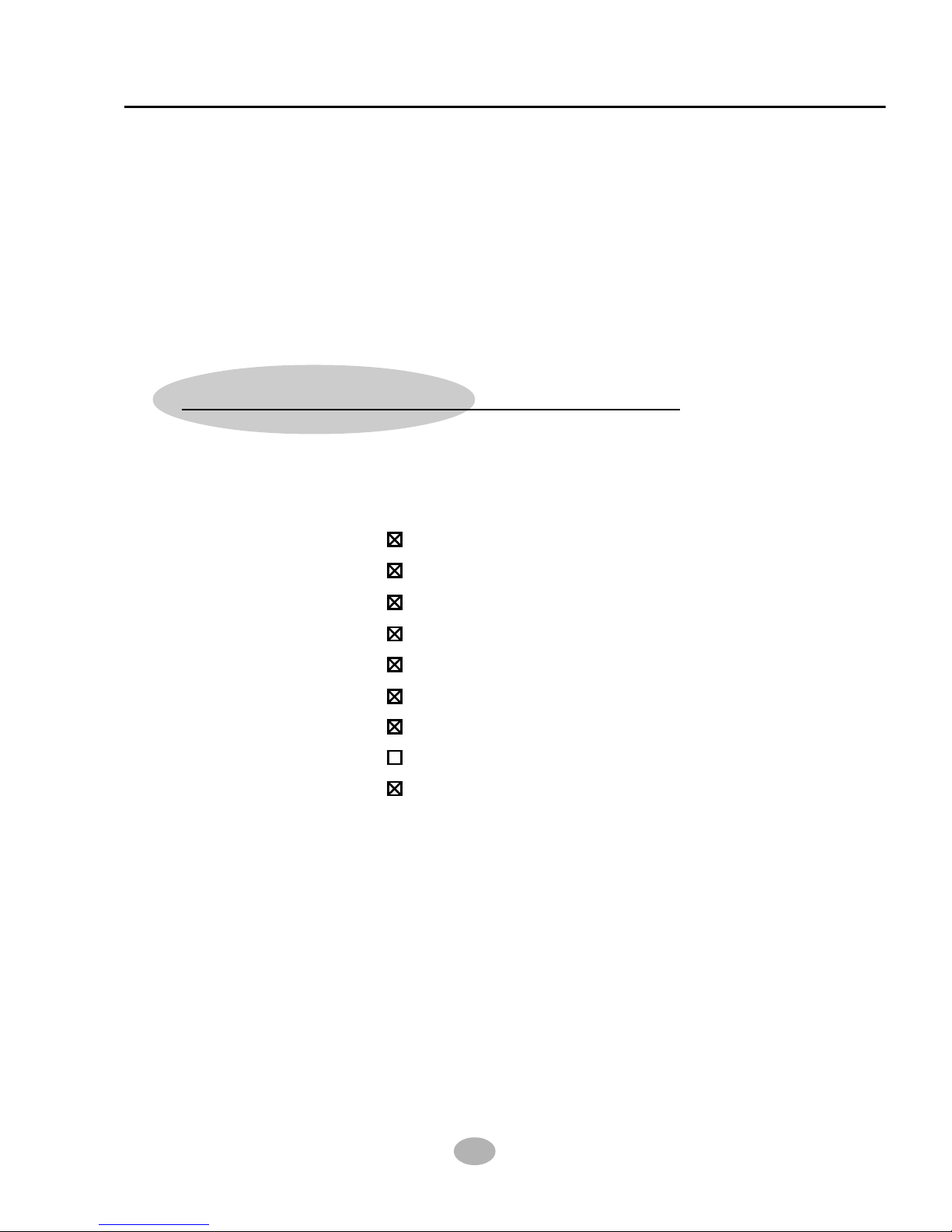
1-2 MAINBOARD LAYOUT
1-2.1 Mainboard Layout --- 75DRV
USB2
1
16
1
16
USB3
CNR 1
FLASH BIOS
USB0
USB1
PS/2
MOUSE
PS/2
K/B
LPT1
COM1COM2
GAME/MIDI PORT
MIC
SW1
ON
DIP
5 4 3 2 1
SW2
ON
DIP
6 5 4 3 2 1
CN1
ON
DIP
1 2 3 4 5
SW3
FAN1
1 3
FAN3
1 3
CON1
SAPK RST PLED SLED
HDD/LED IR PWR SUSPEND
++
--
+
-
16 30
1 15
RT2
SCR1
JBAT1
1 3
JP1
JP2
1 3
1 3
WOL1
1 3
4
1
JCD_IN1
1 3
JP17
PCI 1
PCI 2
PCI 3
PCI 4
PCI 5
SSF1
ZD1
DDR 266
AGP PRO 4X
FDC1
IDE1
IDE2
VIA
VT8233
AC'97
Codec
LPC I/O
Controller
VIA
VT8366
Li
Battery
FAN2
1 3
Clock
Generator
FAN4
1 3
LINE
OUT
LINE
IN
JP18
JP19
1 3
1 3
SOCKET A
RT1
Using non-compliant memory with higher bus clock (over clocking) may
severely compromise the integrity of system.
75DRV/75DRV-X
14
USB2
1
16
1
16
USB3
CNR 1
FLASH BIOS
USB0
USB1
PS/2
MOUSE
PS/2
K/B
LPT1
COM1COM2
GAME/MIDI PORT
MIC
SW1
ON
DIP
5 4 3 2 1
SW2
ON
DIP
6 5 4 3 2 1
CN1
ON
DIP
1 2 3 4 5
SW3
FAN1
1 3
FAN3
1 3
CON1
SAPK RST PLED SLED
HDD/LED IR PWR SUSPEND
++
--
+
-
16 30
1 15
RT2
SCR1
JBAT1
1 3
JP1
JP2
1 3
1 3
WOL1
1 3
4
1
JCD_IN1
1 3
JP17
PCI 1
PCI 2
PCI 3
PCI 4
PCI 5
SSF1
ZD1
DDR 266
AGP PRO 4X
FDC1
IDE1
IDE2
VIA
VT8233
AC'97
Codec
LPC I/O
Controller
VIA
VT8366
Li
Battery
FAN2
1 3
Clock
Generator
FAN4
1 3
LINE
OUT
LINE
IN
JP18
JP19
1 3
1 3
SOCKET A
RT1
VD-¤
TECH
JP10
1 3
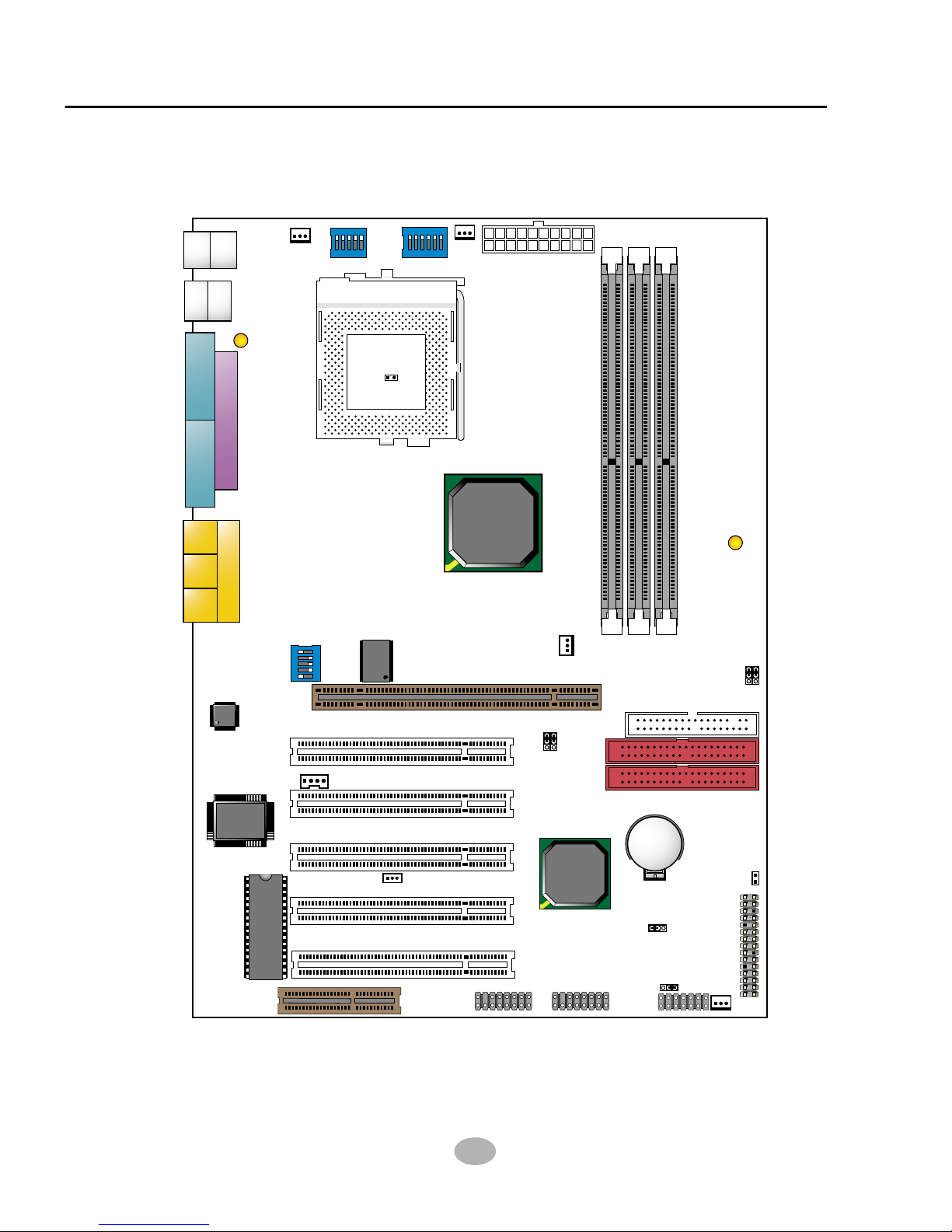
1-2.2 Mainboard Layout --- 75DRV-X
Using non-compliant memory with higher bus clock (over clocking) may
severely compromise the integrity of system.

Chapter 1 Introduction
15
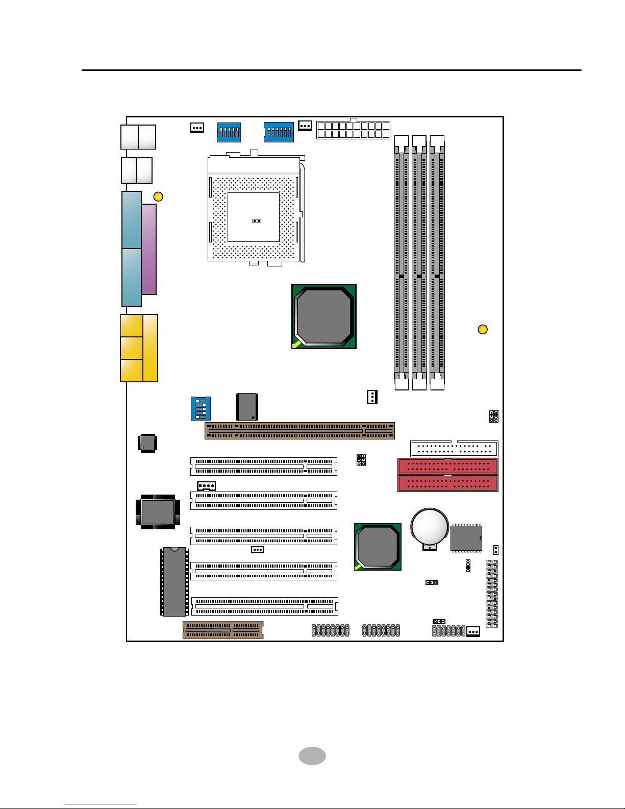
1-3 CHIPSET DIAGRAM--- 75DRV/75DRV-X
• The VT8366 and VT8233 chipset is a high performance, cost-effective and
energy efficient system controller for the implementation of AGP / PCI / ISA
desktop personal computer system based on 64-bit Socket-A (AMD Athlon)
processors.
DDR Vlink
Host North
552 BGA
VT8233
Vlink
Client South
352 BGA
3D
Graphics
Controller
Athlon
Host CPU
SDR/VCM
& DDR
SDRAM
Clock
Buffer
Clock
Generator
SDR/DDR Memory Bus
AGP Bus
SYSCLK, SYSCLK#
INTR, NMI, SM#, STPCLK#,
IGNNE#, FERR#, A20M#,
PWROK, INIT#, RESET#
GCLK
PCLK
PCKRUN#
ATA33/66/100
MII/LAN
6x USB
LPC
SMBus
Power Plan & Peripheral Control
GPIO and ACPI Events
PCI Bus
CKE#
MCLK
HCLK
PCLK
CPUSTP#
PCISTP#
SUSCLK,
SUSST1#
GCKRUN#
Address
Out
CFWDRST
CONNECT
PROCRDY
In
Data
VT8366
Diagram of Apollo Pro266 System Block Using the VT8233 V-Link
South Bridge
 Loading...