

Page 1

AR-B7041
8MB/4MB SOLID STATE DISK
User’ s Guide
Edition: 1.3
Book Number: AR-B7041-99.B01
Page 2

Page 3

AR-B7041 User¡¦s Guide
Table of Contents
0. PREFACE....................................................................................................................................................... 0-2
0.1 COPYRIGHT NOTICE AND DISCLAIMER................................................................................................................................0-2
0.2 WELCOME TO THE AR-B7041 DISK CARD.............................................................................................................................0-2
0.3 BEFORE YOU USE THIS GUIDE...............................................................................................................................................0-2
0.4 RETURNING YOUR BOARD FOR SERVICE............................................................................................................................0-2
0.5 TECHNICAL SUPPORT AND USER COMMENTS...................................................................................................................0-2
0.6 ORGANIZATION..........................................................................................................................................................................0-3
0.7 STATIC ELECTRICITY PRECAUTIONS....................................................................................................................................0-3
1. OVERVIEW..................................................................................................................................................... 1-1
1.1 INTRODUCTION.........................................................................................................................................................................1-1
1.2 PACKING LIST............................................................................................................................................................................1-2
1.3 FEATURES..................................................................................................................................................................................1-2
2. INSTALLATION.............................................................................................................................................. 2-1
2.1 OVERVIEW..................................................................................................................................................................................2-1
2.2 UTILITY DISKETTE – SSD UTILITY..........................................................................................................................................2-1
2.3 WRITE PROTECT FUNCTION...................................................................................................................................................2-4
2.3.1 Hardware Write Protect.......................................................................................................................................................2-4
2.3.2 Software Write Protect ........................................................................................................................................................2-4
2.3.3 Enable the Software Write Protect......................................................................................................................................2-5
2.3.4 Disable the Software Write Protect.....................................................................................................................................2-5
2.4 WATCHDOG TIMER...................................................................................................................................................................2-5
2.4.1 Watchdog Timer Setting......................................................................................................................................................2-6
2.4.2 Watchdog Setting................................................................................................................................................................2-6
2.4.3 Watchdog Timer Enabled....................................................................................................................................................2-6
2.4.4 Watchdog Timer Trigger......................................................................................................................................................2-7
2.4.5 Watchdog Timer Disabled ...................................................................................................................................................2-7
3. SOLID STATE DISK ....................................................................................................................................... 3-1
3.1 OVERVIEW..................................................................................................................................................................................3-1
3.2 SWITCH SETTING......................................................................................................................................................................3-2
3.2.1 Overview..............................................................................................................................................................................3-2
3.2.2 I/O Port Address Select (SW1-1 & SW1-2)........................................................................................................................3-3
3.2.3 SSD Firmware Address Select (SW1-3 & SW1-4).............................................................................................................3-3
3.2.4 SSD Drive Number (SW1-5, SW1-6 & SW1-7)..................................................................................................................3-3
3.2.5 ROM Type Select (SW1-8 & SW1-9)..................................................................................................................................3-5
3.2.6 Write Protected Select (SW1-10)........................................................................................................................................3-5
3.3 JUMPER SETTING .....................................................................................................................................................................3-6
3.3.1 Memory Type Setting (M1 ~ M4 & JP1) .............................................................................................................................3-6
3.3.2 Bus Connector.....................................................................................................................................................................3-8
3.3.3 Battery Setting.....................................................................................................................................................................3-9
3.4 ROM DISK INSTALLATION........................................................................................................................................................3-9
3.4.1 UV EPROM (27Cxxx)..........................................................................................................................................................3-9
3.4.2 Large Page 5V FLASH Disk..............................................................................................................................................3-11
3.4.3 Small Page 5V FLASH ROM Disk....................................................................................................................................3-12
3.4.4 RAM Disk...........................................................................................................................................................................3-14
3.4.5 Combination of ROM and RAM Disk................................................................................................................................3-15
3.5 AR-B7017...................................................................................................................................................................................3-15
3.5.1 Memory Type Setting (JP1 ~ JP4)....................................................................................................................................3-16
3.5.2 Battery Setting...................................................................................................................................................................3-16
3.5.3 Piggy-Back Connector (CN1)............................................................................................................................................3-17
4. SPECIFICATIONS & SSD TYPES SUPPORTED............................................................................................. 4-1
4.1 AR-B7041.....................................................................................................................................................................................4-1
4.2 AR-B7017.....................................................................................................................................................................................4-2
4.3 SSD TYPES SUPPORTED .........................................................................................................................................................4-3
5. MEMORY BANKS & INDEX............................................................................................................................ 5-1
5.1 USING MEMORY BANKS...........................................................................................................................................................5-1
5.2 EXPANDING THE AR-B7041’ S MEMORY CAPACITY.............................................................................................................5-2
5.3 INDEX ..........................................................................................................................................................................................5-5
6. PLACEMENT & DIMENSIONS ........................................................................................................................ 6-1
6.1 PLACEMENT...............................................................................................................................................................................6-1
6.2 DIMENSIONS FOR AR-B7041 ...................................................................................................................................................6-3
0-1
Page 4

AR-B7041 User¡¦s Guide
0. PREFACE
0.1 COPYRIGHT NOTICE AND DISCLAIMER
September 1996
Acrosser Technology makes no representations or warranties with respect to the contents hereof and specifically
disclaims any implied warranties of merchantability or fitness for any particular purpose. Furthermore, Acrosser
Technology reserves the right to revise this publication and to make changes from time to time in the contents
hereof without obligation of Acrosser Technology to notify any person of such revisions or changes.
Possession, use, or copying of the software described in this publication is authorized only pursuant to a valid
written license from Acrosser or an authorized sublicensor.
(C) Copyright Acrosser Technology Co., Ltd., 1996. All rights Reserved.
Acrosser, IBM, IBM PC/XT/AT, MS-DOS, PC-DOS, DR-DOS, X-DOS…are registered trademarks.
All other trademarks and registered trademarks are the property of their respective holders.
This document was produced with Adobe Acrobat 3.01.
0.2 WELCOME TO THE AR-B7041 DISK CARD
This guide introduces the Acrosser AR-B7041 Disk board.
Use the information describes this card’ s functions, features, and how to start, set up and operate your ARB7041. You also could find general system information here.
0.3 BEFORE YOU USE THIS GUIDE
The AR-B7041 diskette provides the newest information about the card. Please refer to the README.DOC file
of the enclosed utility diskette. It contains the modification and hardware & software information, and adding
the description or modification of product function after manual published.
0.4 RETURNING YOUR BOARD FOR SERVICE
If your board requires servicing, contact the dealer from whom you purchased the product for service information.
If you need to ship your board to us for service, be sure it is packed in a protective carton. We recommend that
you keep the original shipping container for this purpose.
You can help assure efficient servicing of your product by following these guidelines:
1. Include your name, address, telephone and facsimile number where you may be reached during the day.
2. A description of the system configuration and/or software at the time is malfunction.
3. A brief description is in the symptoms.
0.5 TECHNICAL SUPPORT AND USER COMMENTS
User’ s comments are always welcome as they assist us in improving the usefulness of our products and the
understanding of our publications. They form a very important part of the input used for product enhancement
and revision.
We may use and distribute any of the information you supply in any way we believe appropriate without incurring
any obligation. You may, of course, continue to use the information you supply.
If you have suggestions for improving particular sections or if you find any errors, please indicate the manual title
and book number.
Please send your comments to Acrosser Technology Co., Ltd. or your local sales representative.
Internet electronic mail to: webmaster@acrosser.com
0-2
Page 5

AR-B7041 User¡¦s Guide
0.6 ORGANIZATION
This information for users covers the following topics (see the Table of Contents for a detailed listing):
l Chapter 1, “Overview,” provides an overview of the system features and packing list.
l Chapter 2, “Installation,” describes the utility diskette using, solid state disk’ s writing protect function, and
the watchdog timer.
l Chapter 3, “Solid State Disk,” describes the various type SSD’ s installation steps and how to adjust the
jumper, and the connectors setting.
l Chapter 4, Specifications & SSD Types Supported
l Chapter 5, Memory Banks & Index
l Chapter 6, Placement & Dimensions
0.7 STATIC ELECTRICITY PRECAUTIONS
Before removing the board from its anti-static bag, read this section about static electricity precautions.
Static electricity is a constant danger to computer systems. The charge that can build up in your body may be
more than sufficient to damage integrated circuits on any PC board. It is, therefore, important to observe basic
precautions whenever you use or handle computer components. Although areas with humid climates are much
less prone to static build-up, it is always best to safeguard against accidents may result in expensive repairs. The
following measures should generally be sufficient to protect your equipment from static discharge:
• Touch a grounded metal object to discharge the static electricity in your body (or ideally, wear a grounded
wrist strap).
• When unpacking and handling the board or other system component, place all materials on an antic static
surface.
• Be careful not to touch the components on the board, especially the “golden finger” connectors on the bottom
of every board.
0-3
Page 6

Page 7
AR-B7041 User¡¦s Guide
1. OVERVIEW
This chapter provides an overview of your system features and capabilities. The following topics are covered:
l Introduction
l Packing List
l Features
1.1 INTRODUCTION
The AR-B7041 is a solid state disk card that can be used as the system disk or as a replacement for mechanical
disk drives is any IBM PC/XT/AT or compatible computer. It is ideal for, but not limited to, the following
applications:
l Diskless PC workstations
l High reliability and/or high speed access applications
l Heavy duty disk access requirements
l PC controller for industrial or line test instruments
l Environments hostile to standard floppy disks & drives (Dust, moisture, vibration, etc.)
This card is a byte wide memory card that plugs into any free slot of system. Eight 32-pin JEDEC DIP sockets
may be populated with up to 8MB of EPROM, 4MB of FLASH EPROM/SRAM or combinations of them. The ARB7041 also provides one piggyback connector to install AR-B7017 cards (4MB ROM/RAM/FLASH module), for
maximum of 12MB disk space.
Data retention of SRAM is ensured by an on-board Lithium battery or using an external battery pack that may be
connected to the AR-B7041. A write protect function allows you to prevent data on SRAM disk or FLASH disk
from accidental deletion or overwrite.
The AR-B7041 and AR-B7017 supports 5V FLASH EPROMs. This enables you to program FLASH EPROMs onboard directly. If small page (less or equal to 512 bytes per page) 5V FLASHs are used, you can format FLASH
disk and copy files onto the FLASH disk just like using a normal disk. This feature will extend the life of your
FLASH EPROM chips by only reprogram a small area. You should use all of the related DOS command (such as
COPY, DEL, …etc.) to update files on the 5V FLASH disk.
The AR-B7041 ROM/RAM disk card is extremely easy to install and use. However, it is advised that you read this
manual before you begin to install.
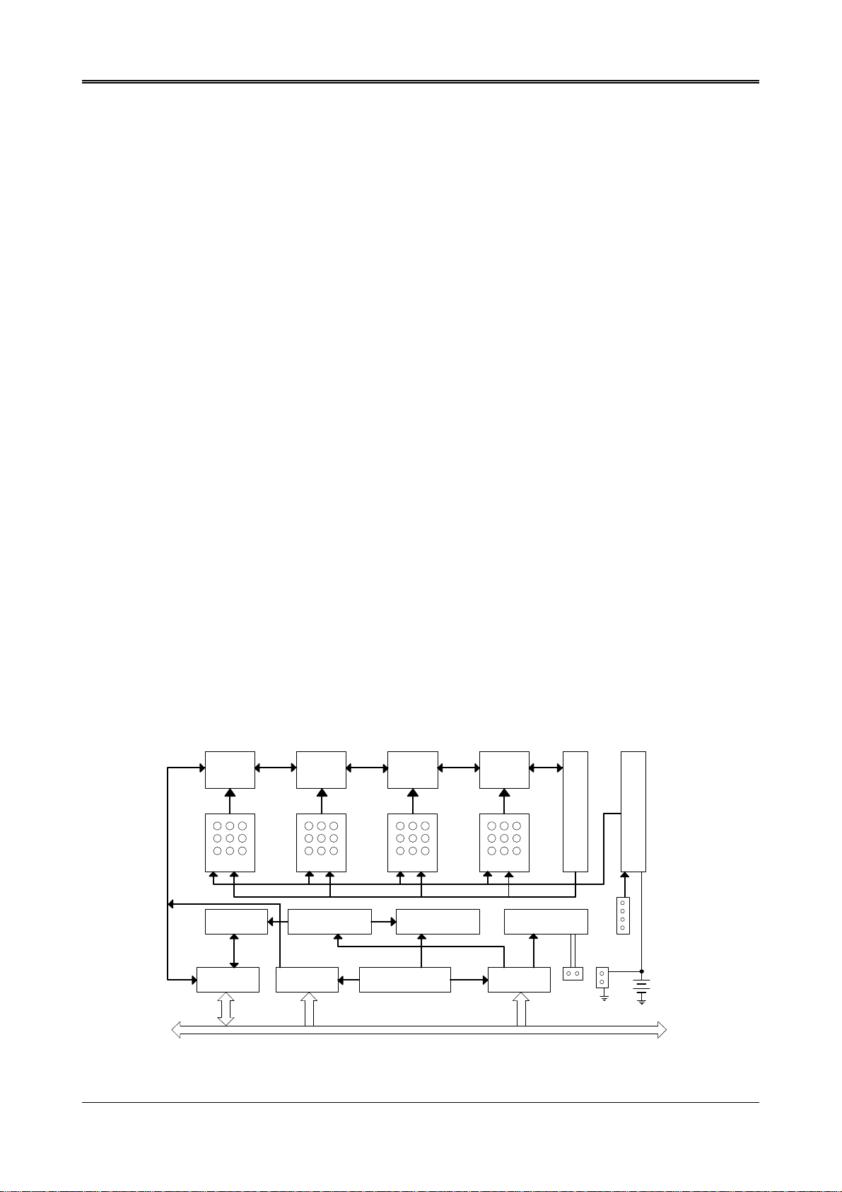
MEM1
MEM2
M1 M2 M3 M4
ROM DISK
BIOS
ADDRESS AND
DATA BUFFER
MEM3
MEM4
I/O BUFFER
AND LATCH
MEMORY
DECODER
MEM5
MEM6
FLASH EPROM
VPP GENERATOR
1 2 3 4 5 6 7 8 9 10
SW1
MEM7
MEM8
WATCHDOG TIMER
I/O DECODER
CN1
J1
J5
J4
BAT1
ISA BUS
Figure 1-1 AR-B7041 Functional Block Diagram
1-1
Page 8

AR-B7041 User¡¦s Guide
1.2 PACKING LIST
The accessories are included with the system. Before you begin installing your AR-B7041 board, take a moment
to make sure that the following items have been included inside the AR-B7041 package.
l The quick setup manual
l 1 AR-B7041 solid state disk card
l 1 Software utility
If you purchased an AR-B7017, please check that the following items have been included in the AR-B7017
package.
l 1 AR-B7017 ROM/RAM disk card
l 6 Mounting screws (2 for spare)
l 3 Mounting standoffs (1 for spare)
l 1 2-wired battery cable
NOTE: If there are any discrepancies, please contact your Acrosser distributor immediately.
1.3 FEATURES
The system provides a number of special features that enhance its reliability, ensure its availability, and improve its
expansion capabilities, as well as its hardware structure.
l ISA bus add-on card designed for PC/XT, PC/AT systems.
l Fully compatible with standard floppy disk drive
l Eight 32-pin JEDEC DIP sockets
l Maximum capacity of 8MB EPROM, 4MB FLASH/SRAM or combinations
l One AR-B7017 piggy back modules can be carried by AR-B7041 and have a maximum of 12MB
disk capacity
l Accepts 128Kx8 to 1Mx8 EPROM
l Accepts 64Kx8 to 512Kx8 5V FLASH EPROM
l Accepts 128Kx8 to 512Kx8 SRAM
l Software and hardware write protect functions
l 850mAH Lithium battery for SRAM data retention. External battery connector also included
l Supports on-board FLASH EPROM programmer and programming utility
l Switch selectable drive unit (8 combinations of A:, B:, C: or D:)
l Switch selectable of I/O and memory address. Occupies only 4 I/O address and 16KB memory
address
l Programmable watchdog timer
l LED indicator for disk data access and watchdog timer status
1-2
Page 9

AR-B7041 User¡¦s Guide
2. INSTALLATION
This chapter describes the procedure of the utility diskette installation. The following topics are covered:
l Overview
l Utility Diskette
l Write Protect Function
l Watchdog Timer
2.1 OVERVIEW
This chapter provides information for you to set up a working system based on the AR-B7041 card. Please read
the details of the card’ s hardware descriptions before installation carefully, especially jumpers’ setting, switch
settings and cable connections.
When you install the card please notice the following item:
1. Make sure the base I/O address does not conflict with other I/O cards.
2. Make sure the memory address not conflict with other memory cards.
3. Make sure the jumper settings for the memory are all installed properly.
4. Don’ t use the invalid shadow RAM address.
5. Prevent to use the same range of memory address as the AR-B7041 used, if you have install EMS driver.
6. If you are using the MS-DOS 6.2 to format SRAM or 5V FLASH EPROM disk, you might get some bad
sectors in your ROM/RAM disk. This will reduce the capacity of your FLASH/SRAM disk. To solve this
problem, please type:
C:\>FORMAT [drive number] /U/C
or
C:\>FORMAT [drive number] /U/C/S
2.2 UTILITY DISKETTE – SSD UTILITY
To support the AR-B7041 solid state disk’ s operations, the following files have been provided on the enclosed
diskette.
(A) PGM7041.EXE
PGM7041.EXE PGM7041.EXE is used to program the 12V FLASH EPROM after the ROM pattern files are
generated by RFG.EXE The PGM7041.EXE can also program the correctness of the ROM
pattern files onto 5V FLASH EPROM (start from MEM1) or SRAM for testing the ROM pattern
files.
To execute PGM7041.EXE, the main menu will be displayed on your screen. There are 8 options on the main
menu.
Quit to DOS
Quits and exits to the DOS.
OS Shell
Exits from PGM7041 temporarily to the DOS prompt. Type EXIT to return to PGM7041 main menu.
Load ROM File
If this option is used, the PGM7041 will prompt you for the ROM pattern file name. This option is useful if
you have not previously entered a ROM pattern file name or if you wish to use a different ROM pattern file.
The PGM7041 will check and display the ROM file name, ROM file size, (FLASH) memory capacity and the
number of ROM pattern files that will be loaded and copied onto the (FLASH) memory chips.
2-1
Page 10

AR-B7041 User¡¦s Guide
Verify Memory
If ROM pattern files were loaded without error, this option instructs PGM7041 to verify the contents of
(FLASH) memory chips with the current ROM pattern files.
Program Memory
If there are no mistakes in your ROM pattern file, then this menu option will erase (FLASH) memory, write
the current ROM pattern files onto (FLASH) memory and verify data that was just written to (FLASH)
memory, using the ROM pattern files.
Memory Type/Mfr.
Before you program the (FLASH) memory chips, make sure that the FLASH’ s type and manufactory match
the one shown on the main menu. Otherwise, you can use this option to select the proper type and
manufacture and instruct the program to use a right programming algorithm.
Select PGM Chips
Normally the PGM7041 will program all ROM pattern files onto the FLASH memories with the ROM pattern
files just loaded. But you can use this option to select which memory chips that you want to program and
which memory chips need to be skipped. The PGM7041 will only program the selected chips when writing
data to the FLASH memory. This is very useful when some of the memory chip were verified and
programmed previously.
Select FLASH PLSCNTs
If the 12V FLASHs have been programmed several times, please select the <Slowest> FLASH PLSCNT
mode instead of <Standard> mode. In the <Slower> or <Slowest> mode, PGM7041.EXE will retry more
times to program data onto the 12V FLASHs correctly. The default setting is <Slowest> mode.
Move the reverse video bar to the “Program Memory” option then press ENTER. PGM7041 will write the ROM
pattern files onto the (FLASH) memories. Ensure that data is verified by the PGM7041 correctly.
(B) SWAP41.EXE
SWAP41.EXE This program demonstrates how to reassigns your AR-B7041 card to the drive unit set by
SW1-5, SW1-6 and SW1-7. This file should be executed in the first line of your
<AUTOEXEC.BAT> file.
(C) AUTOEXEC.BAT
AUTOEXEC.BAT This is a sample batch file to illustrate how to create an <AUTOEXECT.BAT> file, if you are
planning to use the AR-B7041 as a boot drive.
(D) RFG.EXE
RFG.EXE This program is used to generate ROM pattern files in a binary format. Each ROM pattern file
has the same size as the FLASH or EPROM and can be easily programmed on to the FLASH
with on-board programmer or on to EPROM with any EPROM programmer. If you have
specified a DOS drive in the *.PGF file, RFG will generate bootable ROM pattern files for the
EPROM or FLASH disk. The RFG supports the following DOS: MS-DOS, PC-DOS, DR-DOS,
and X-DOS.
NOTE: If you want to use AR-B7041 with any DOS which is not supported by RFG, please send your requirement
to Acrosser Technology Co., Ltd. or contract with your local sales representative.
The RFG.EXE provided in the utility diskette is a program that converts the files you list in the PGF and convert
them into ROM pattern file. The RFG will determine how many EPROMs are needed and generate the same
number of ROM pattern files. These ROM pattern files are named with the name assigned by the ROM_NAME in
the PGF and the extension names are *.R01, *.R02….etc. To generate ROM pattern files.
The ROM File Generator main menu will be displayed on the screen. There are 7 options on the main menu. They
serve the following functions:
2-2
Page 11

AR-B7041 User¡¦s Guide
Quit to DOS
Quits and exits to the DOS
OS Shell
Exits from the RFG temporarily to the DOS prompt. Type <EXIT> to return to the RFG main menu.
Load PFG File
If this option is used, the RFG will prompt you for the PGF file name. This option is useful if you have not
previously entered a PGF name or you wish to use a different PGF file. The RFG will check and display the
PGF filename, ROM pattern file name, EPROM capacity, DOS version and the number of ROM pattern files
that will be generated.
Type Current PGF File
This option instructs the RFG to use the DOS type command to display the contents of the current PGF file.
Generate ROM File(s)
If there is no mistake in your *.PGF file, then this menu option will generate ROM pattern files. The number
of ROM pattern file generated by the RFG will depend on the total capacity needed by your files. For
instance, if 3 files are generated, then you will need to use 3 EPROMs (The size depends upon the number
stated in your PGF). The ROM pattern files will have the same file names, but will have different extension
names. For example:
TEST.R01, TEST.R02, TEST.R03…etc.
Display Error in PGF File
This option displays errors that were detected in your PGF.
Help to PGF File
This option gives information on how to write a PGF file and how to generate ROM pattern files. An
example PGF is also included.
Move the reverse video bar to <Generate ROM File(s)> then press [ENTER]. The ROM pattern file is a binary file.
The file size will be the same size as the EPROM that you assigned in the PGF. For example, if you are using
128KX8 EPROM memory chips, then the size of ROM patterns file will be 131072 bytes. For other chips the file
size will be:
64KX8 EPROM----65536 bytes
256KX8 EPROM—262144 bytes
512KX8 EPROM---524288 bytes
1MX8 EPROM -----1048576 bytes
(E) RFGDEMO.PGF
RFGDEMO.PGF This file provides a sample PROGRAM GROUP FILE which illustrates how to create ROM
pattern files correctly.
The PGF is an ASCII text file that can be created by using any text editor, word processor or DOS <COPY CON>
command. The PGF lists what files will be copied and if DOS is going to be copied. This file can have any DOS
filename, but the extension name must be *.PGF. For example, followings are valid filenames.
RFGDEMO.PGF
MYRFG.PGF
MSDOS.PGF
….
2-3
Page 12

AR-B7041 User¡¦s Guide
An examples of the *.PGF file is as follow.
ROM_NAME=TEST1 ; ROM pattern file name is TEST1
; The output file names will be TEST1.R01, TEST1.R02..etc.
DOS_DRIVE=C: ; DOS system drive unit is drive C:
; If user does not want to copy DOS system files onto the ROM disk
; write as DOS_DRIVE=NONE
ROM_SIZE=128 ; 128 means 128KX8 (27C/29F010) EPROM size used
; 256 means 512KX8 (27C/29F020) EPROM size used
; 512 means 512KX8 (27C/29F040) EPROM size used
; 1024 means 1MX8 (27C080) EPROM size used
The following 3 files are options which depend on whether the ROM disk is to be bootable or not.
CONFIG.SYS
AUTOEXEC.BAT
SWAP41.EXE
; Below are user’ s files
A:\USER1.COM ; File USER1.COM on root of drive A:
USER2.EXE ; File USER2.EXE on current directory & drive
C:\TTT\USER3.TXT ; File USER3.TXT on sub-directory TTT of drive C:
(F) WD7041.EXE
WD7041.EXE This program demonstrates how to enable and trigger the watchdog timer. It allows you to
test the <TIMES-OUT & RESET> function when the watchdog timer is enabled.
(G) WP7041.EXE
WP7041.EXE This program demonstrates how to enable and disable software write protected function. It
also shows the current protect mode of write or read only memory.
2.3 WRITE PROTECT FUNCTION
The AR-B7041 provides hardware and software write protect functions for small page 5V FLASH disk and only
software write protected function for SRAM disk. This is to prevent your data on 5V FLASH or SRAM disk from
accidental deletion or overwrite. If your FLASH/SRAM disk is write protected, any write operation to the protected
FLASH/SRAM disk will get a write protect error:
Write protect error writing drive A
About, Retry, Fail?
2.3.1 Hardware Write Protect
To enable the hardware protect function for small page 5V FLASH disk set the SW1-8 and SW1-9 to the ON and
OFF position, please refer to the “Switch Setting”.
2.3.2 Software Write Protect
If you need the write protect function and sometimes you have to write or update data on your FLASH/SRAM disk,
you can use the software write protect instead of hardware write protect. The software write protect function is
enabled or disabled by writing a data to an I/O port.
2-4
Page 13
2.3.3 Enable the Software Write Protect
Write 80h to the base port+0 address
Example 1: (in assembly language)
MOV DX, 220H ; If the AR-B7041’ s base I/O address is 220H
MOV AL, 80H ; Enable byte = 80h
OUT DX, AL
Example 2: (in BASICA language)
OUT &H220, &H80; REM If the AR-B7041’ s base I/O address is 220h
Example 3: (in Turbo C language)
outportb(0x220,0x80); /*If the AR-B7041’ s base I/O address is 220h*/
2.3.4 Disable the Software Write Protect
Write 0 to the base port+0 address
Example 1: (in assembly language)
MOV DX, 220H ; If the AR-B7041’ s base I/O address is 220h
MOV AL, 00H ; Disable byte=00h
OUT DX, AL
AR-B7041 User¡¦s Guide
Example 2: (in BASICA language)
OUT &H220, &H00; REM If the AR-B7041’ s base I/O address is 220h
Example 3: (in Turbo C language)
outportb(0x220,0x00); /*If the AR-B7041’ s base I/O address is 220h*/
2.4 WATCHDOG TIMER
This section describes how to use the Watchdog Timer, disabled, enabled, and trigger.
The AR-B7041 is equipped with a programmable time-out period watchdog timer. User can use the program to
enable the watchdog timer. Once you have enabled the watchdog timer, the program should trigger it every time
before it times out. If your program fails to trigger or disable this timer before it times out because of system hangup, it will generate a reset signal to reset the system. The time-out period can be programmed to be 3 to 42
seconds.
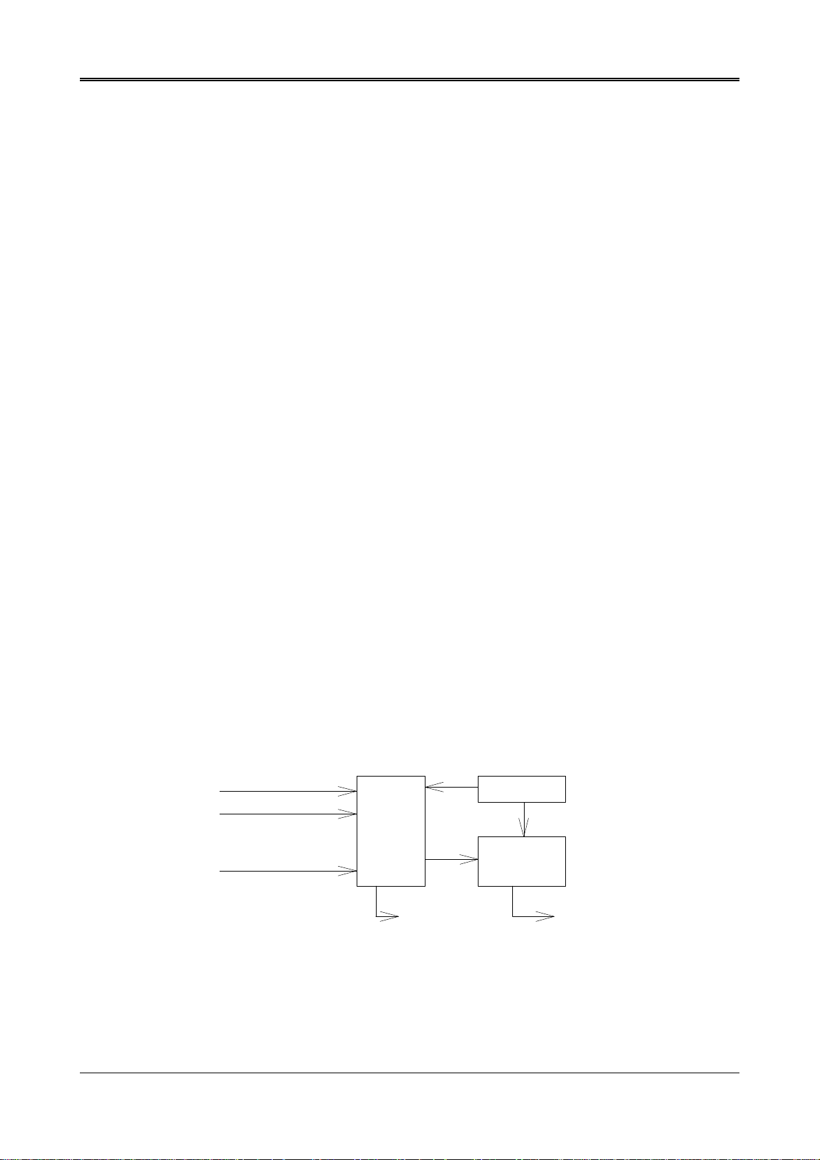
Enable (D7)
Time Factor (D0-D2)
Watchdog
Register
Write and Trigger
Watchdog
LED
Figure 2-1 Watchdog Block Diagram
Time Base
Counter
and
Compartor
RESET
2-5
Page 14
AR-B7041 User¡¦s Guide
2.4.1 Watchdog Timer Setting
The watchdog timer is a circuit that may be used from your program software to detect crashes or hang-ups.
Whenever the watchdog timer is enabled, the LED will blink to indicate that the timer is counting. The watchdog
timer is automatically disabled after reset.
Once you have enabled the watchdog timer, your program must trigger the watchdog timer every time before it
times-out. After you trigger the watchdog timer, it will be set to zero and start to count again. If your program fails
to trigger the watchdog timer before time-out, it will generate a reset pulse to reset the system.
The factor of the watchdog timer time-out constant is approximately 6 seconds. The period for the watchdog timer
time-out period is between 1 to 7 timer factors.
If you want to reset your system when watchdog times out, the following table listed the relation of timer factors
between time-out period.
Time Factor Time-Out Period (Seconds)
80H 3
81H 6
82H 12
83H 18
84H 24
85H 30
86H 36
87H 42
Table 2-1 Time-Out Setting
2.4.2 Watchdog Setting
(1) Reset Signal Output of Watchdog Timer (J1)
J1 is used to connect to reset header of main board or CPU card.
J1
1 2
Figure 2-2 J1: Reset Signal Output of Watchdog Timer
1 -WDRST
2 -WDRST
(2) Watchdog LED Header (J2)
J2
1 2
Figure 2-3 J2: Watchdog LED Header
1 LED+
2 LED-
2.4.3 Watchdog Timer Enabled
To enable the watchdog timer, you have to output a byte of timer factor to the watchdog register whose address is
base port+3m 76h or 77h. The following is a BASICA program which demonstrates how to enable the watchdog
timer and set the time-out period at 24 seconds.
1000 REM Points to command register
1010 WD_REG% = BASE_PORT% + 3
1020 REM Timer factor = 84H
1030 TIMER_FACTOR% = %H84
1040 REM Output factor to watchdog register
1050 OUT WD_REG%, TIMER_FACTOR%
.,etc.
2-6
Page 15

AR-B7041 User¡¦s Guide
2.4.4 Watchdog Timer Trigger
After you enable the watchdog timer, your program must write the same factor as enabling to the watchdog register
at least once every time-out period to its previous setting. You can change the time-out period by writing another
timer factor to the watchdog register at any time, and you must trigger the watchdog before the new time-out period
in next trigger. Below is a BASICA program which demonstrates how to trigger the watchdog timer:
2000 REM Points to command register
2010 WD_REG% = BASE_PORT% + 3
2020 REM Timer factor = 84H
2030 TIMER_FACTOR% = &H84
2040 REM Output factor to watchdog register
2050 OUT WD_REG%, TIMER_FACTOR%
.,etc.
2.4.5 Watchdog Timer Disabled
To disable the watchdog timer, simply write a 00H to the watchdog register.
3000 REM Points to command register
3010 WD_REG% = BASE_PORT% + 3
3020 REM Timer factor = 0
3030 TIMER_FACTOR% = 0
3040 REM Output factor to watchdog register
3050 OUT WD_REG%, TIMER_FACTOR%
., etc.
2-7
Page 16

Page 17

AR-B7041 User¡¦s Guide
3. SOLID STATE DISK
The section describes the various type SSDs’ installation steps as follows. This chapter describes the procedure of
the installation. The following topics are covered:
l Overview
l Switch Setting
l Jumper Setting
l ROM Disk Installation
l AR-B7017
3.1 OVERVIEW
Eight 32-pin JEDEC memory sockets on the AR-B7041 can be populated with up to 8MB of EPROM, 4MB of
FLASH, 4MB of SRAM or combinations the EPROM/SRAM or FLASH/SRAM. Each socket accepts the following
memory chips:
EPROM: 27C080 (1Mx8), 27C040 (512Kx8), 27C020
(256Kx8) and 27C010 (128Kx8)
Small Page 5V FLASH: 29C040A (512Kx8), 29C040 (512Kx8),
29C020 (256Kx8), 29C010 (128Kx8),
29C512 (64Kx8), 28EE010 (128Kx8),
28EE011 (128Kx8), 29EE010 (128Kx8),
29EE011 (128Kx8) and 28SF040 (512Kx8)
Large Page 5V FLASH: 29F040 (512Kx8), 29F020 (256Kx8),
29F010 (128Kx8) and 29F512 (64Kx8)
SRAM: 584000 (512Kx8), 581000(128Kx8)
The AR-B7041 uses a 3.6volt Lithium non-chargeable battery to backup stored data in the SRAM memory when
the power is off. Please use low power SRAM chips for a longer data retention period. (These SRAM chips are
usually designated with a <L> in the chip model code.)
3-1
Page 18

AR-B7041 User¡¦s Guide
3.2 SWITCH SETTING
We will show the locations of the AR-B7041 switch, and the factory-default setting.
CAUTION: The switch setting needs to adjust with the jumpers setting, make sure the jumper settings and the
switch setting are correct.
WD
+
U11
SW1
J2
1
++-
J3
J4
LED2LED1
JP2
1
EC
BAT-OUT
1
J5
1
2
M2
3
A B C
U4 U5 U6
MEM2MEM3MEM4
1
2
3
A
B C
M1
P1
P3P4
P2
1
JP1
J1
RST
U10
U7
MEM1
U8
U9
U12
EN
NC
+
+
-
J6
U17
U21
CN1
U13 U14 U15
MEM8 MEM7
MEM6 MEM5
U16
U19
U24
U26
M4
A B C
1
2
3
M3
A
CB
P6
1
2
3
P5
H9H2
P8
P7
H8
H7H6H5
H3
Figure 3-1 AR-B7041 Jumper & Connector Location
3.2.1 Overview
There is 1 DIP Switch located on the AR-B7041. It performs the following functions:
ON
OFF
1 2 3 4 5 6
Figure 3-2 SW1: Switch Select
7 8 9 10
U18
U22
U25
U27
BAT1
BUS1
3-2
SW1-1 & SW1-2 Set the base I/O port address
SW1-3 & SW1-4 Set the starting memory address
SW1-5, SW1-6 &
SW1-7
Set the drive number of solid state
disk
SW1-8 & SW1-9 Set the used ROM memory chips
SW1-10 ROM disk write protected function
Page 19

AR-B7041 User¡¦s Guide
3.2.2 I/O Port Address Select (SW1-1 & SW1-2)
SW1-1 and SW1-2 are provided to select one of the four base port addresses for the watchdog timer and the solid
state disk. The AR-B7041 occupies 4 I/O port addresses. The following state selections of base port address.
SW1-1 SW1-2 Base Port Solid State Disk Watchdog
OFF (*) OFF 220h 220h-222h 223h & 76h-77h
ON OFF 2A0h 2A0h-2A2h 2A3h & 76h-77h
OFF ON 320h 320h-322h 323h
ON ON 3A0h 3A0h-3A2h 3A3h
Table 3-1 I/O Port Address Select
3.2.3 SSD Firmware Address Select (SW1-3 & SW1-4)
The AR-B7041’ s SSD firmware occupies 16KB of memory. SW1-3 and SW1-4 are used to select the memory
base address. You must select an appropriate address so that the AR-B7041 will not conflict with memory
installed on other add-on cards. Do not to use the shadow RAM area or EMM driver page frame in this area.
SW1-3 SW1-4 Firmware Address Bank Memory Address
OFF (*) OFF CC00:0 (8KB) CE00:0 (8KB)
ON OFF D000:0 (8KB) D200:0 (8KB)
OFF ON D400:0 (8KB) D600:0 (8KB)
ON ON D800:0 (8KB) DA00:0 (8KB)
Table 3-2 SSD Firmware Address Select
If you are going to install the EMM386.EXE driver, please use the [X] option to prevent EMM386.EXE from using
the particular range of segment address as an EMS page which is used by AR-B7041. For example, write a
statement in the CONFIG.SYS file as follow: (If the memory configuration of AR-B7041 is CC00:0)
DEVICE=C:\DOS\EMM386.EXE X=CC00-CFFF
3.2.4 SSD Drive Number (SW1-5, SW1-6 & SW1-7)
The AR-B7041 can simulate one or two disk drives. You can assign the drive number of AR-B7041 by configure
SW1-5, SW1-6 & SW1-7.
If you have copied DOS to the ROM/RAM disk, the computer will always boot from the ROM/RAM disk. After the
DOS is booted, the first disk number will be A: until the program SWAP41.EXE is executed. The SWAP41.EXE
changes the drive number according to the setting of SW1-5, SW1-6 & SW1-7.
If your AR-B7041 does not have DOS and is not assigned as drive A, the computer will boot from your hard disk or
floppy disk. In this case, the BIOS of AR-B7041 will set the drive number of ROM/RAM disk to desired drive
number automatically without having to run SWAP41.EXE after system booting. Do not assign the AR-B7041 with
drive 0 (drive A: ) when the ROM/RAM disk does not have DOS. This is just like that you put a non-DOS disk in
the floppy disk.
If you install only one kind of memory chip on the ROM/RAM disk, the AR-B7041 will simulate one disk drive.
SW1-5 SW1-6 SW1-7 Occupies floppy disk number (SSD)
OFF OFF OFF 0 (Note 1)
ON OFF OFF 1
OFF ON OFF 2
ON ON OFF 3
OFF OFF ON 0
ON OFF ON 0
OFF ON ON 0 or 1 (Note 2)
ON ON ON 0 or 2 (Note 3)
Table 3-3 SSD Drive Number
3-3
Page 20

AR-B7041 User¡¦s Guide
NOTE: 1. Factory preset
2. If there is no DOS on this ROM/RAM disk, the disk number will be 1. If any DOS is found by the ARB7041 BIOS, the disk number will be 0. But, you can change the disk number from 0 to 1 by pressing
<ESC> key during system boot-up.
3. If there is no DOS on this SSD, the disk number will be 2 (C: or D: or…). If any DOS is found by ARB7041 SSD BIOS, the disk number will be 0 (A:). But, you can change the disk number from 0 to 2 by
pressing the <ESC> key during system bootup.
(1) Simulate 2 Disk Drive
When (FLASH) EPROM and SRAM are used on the AR-B7041, or you only have installed SRAM that does not
start from MEM1 socket, the AR-B7041 will simulate two disk drives. The drive numbers respect to those switch
settings when AR-B7041 simulates two disk drives.
SW1-5 SW1-6 SW1-7
OFF OFF OFF 0 1
OFF ON OFF 2 3
OFF OFF ON 0 2
OFF ON ON 0 or 1 (Note 2) 1
Table 3-4 SSD Drive Number for Simulate 2 Disk Drive
NOTE: 1. Factory preset
2. If there is no DOS on this ROM/RAM disk, the disk number will be 1. If any DOS is found by the ARB7041 BIOS, the disk number will be 0. But, you can change the disk number from 0 to 1 by pressing
<ESC> key during system boot-up.
3. If there is no DOS on this SSD, the disk number will be 2 (C: or D: or…). If any DOS is found by ARB7041 SSD BIOS, the disk number will be 0 (A:). But, you can change the disk number from 0 to 2 by
pressing the <ESC> key during system bootup.
Occupies floppy disk number
FLASH (EPROM) SRAM
ON OFF OFF 1 2
ON ON OFF 3 Disable (Note 4)
ON OFF ON 0 3
ON ON ON 0 or 2 (Note 3) 2
3-4
4. ROM and RAM disks can not exist simultaneously if the disk number starts from 3.
Page 21

AR-B7041 User¡¦s Guide
(2) Disk Drive Name Arrangement
If any logical hard disk drives exist in your system, there will also be a different disk number depending on which
version DOS you are using.
The solid state disk drive number with there respective DOS drive designation are listed in table as follows. The
solid state disk drive number is changeable as the DOS version. The following table expresses the variety.
Condition
No Logical hard disk A: B: C: D: -- -- -- --
1 Logical hard disk A: B: C: D: E: -- -- -2 Logical hard disk A: B: C: D: E: F: -- -3 Logical hard disk A: B: C: D: E: F: G: -4 Logical hard disk A: B: C: D: E: F: G: H:
Table 3-5 SSD Drive Number for DOS Version before 5.0
Condition
No Logical hard disk A: B: C: D: -- -- -- --
1 Logical hard disk A: B: D: E: C: -- -- -2 Logical hard disk A: B: E: F: C: D: -- -3 Logical hard disk A: B: F: G: C: D: E: -4 Logical hard disk A: B: G: H: C: D: E: F:
Table 3-6 SSD Drive Number for DOS Version 5.0 and Newer
Floppy disk No. Logical hard disk
0 1 2 3 1 2 3 4
Floppy disk No. Logical hard disk
0 1 2 3 1 2 3 4
3.2.5 ROM Type Select (SW1-8 & SW1-9)
SW1-8 & SW1-9 are used to select the memory type of ROM disk which is going to be used on the AR-B7041.
SW1-8 SW1-9 EPROM Type
OFF OFF UV EPROM (27Cxxx)
ON OFF 5V FLASH 29Fxxx
OFF ON 5V FLASH (29Cxxx & 28Eexxx)
ON ON 12V FLASH (28Fxxx)
Table 3-7 ROM Type Select
NOTE: It is also used to perform the hardware write protection of small page 5V FLASH (29Cxxx…etc.) disk.
3.2.6 Write Protected Select (SW1-10)
SW1-10 is used to enable or disable the write protect function of the SRAM disk or small page 5V FLASH disk. If
SW1-10 is set to the <ON> position, the FLASH/SRAM disk will operate in the same manner as a write protected
floppy disk. A write protect floppy disk is a <read only> disk. This function will protect your important file(s) from
accidental deletion.
SW1-10 Disk Access
OFF Read/Write
ON Read Only
Table 3-8 Write Protected Select
3-5
Page 22

AR-B7041 User¡¦s Guide
3.3 JUMPER SETTING
Jumper pins allow you to set specific system parameters. Set them by changing the pin location of jumper blocks.
(A jumper block is a small plastic-encased conductor [shorting plug] that slips over the pins.) To change a jumper
setting, remove the jumper from its current location with your fingers or small needle-nosed pliers. Place the
jumper over the two pins designated for the desired setting. Press the jumper evenly onto the pins. Be careful not
to bend the pins.
We will show the locations of the AR-B7041 jumper pins, and the factory-default setting.
CAUTION: Do not touch any electronic component unless you are safely grounded. Wear a grounded wrist strap
or touch an exposed metal part of the system unit chassis. The static discharges from your fingers can
permanently damage electronic components.
3.3.1 Memory Type Setting (M1 ~ M4 & JP1)
Before installing the memory into memory sockets MEM1 through MEM8 you have to configure the memory type
which will be used (ROM/RAM) on the AR-B7041 card. Each jumper selects the memory type of four continuous
sockets.
You can configure the AR-B7041 as a (FLASH) EPROM disk (ROM only), a SRAM disk (SRAM only) or a
combination of (FLASH) EPROM and SRAM disk.
It is not necessary to insert memory chips into all of the sockets. The number of SRAM chips required depends on
your RAM disk capacity. The number of EPROM chips required depends on the total size of files that you plan to
copy onto the ROM disk and whether or not it will be bootable.
Insert the first memory chip into MEM1 if you are going to configure it as a ROM or SRAM disk. If you use a
combination of ROM and RAM, then insert the (FLASH) EPROM chip starting with the MEM1, and insert the
SRAM chips starting from the first socket which is configured as SRAM.
l M1: is used to configure the memory type of MEM1 to MEM2
l M2: is used to configure the memory type of MEM3 to MEM4
l M3: is used to configure the memory type of MEM5 to MEM6
l M4: is used to configure the memory type of MEM7 to MEM8
CAUTION: When the power is turned off, please note the following precautions.
1. If your data has been stored in the SRAM disk, do not change the jumper position or data will be
lost.
2. Make sure jumpers are set properly. If you mistakenly set the jumpers for SRAM and you have
EPROM or FLASH installed, the EPROM or FLASH will drain the battery’ s power.
3-6
Page 23

EPROM (128KX8, 256KX8 and 512KX8)
5V FLASH (64KX8, 128KX8 and 256KX8)
A B C
1
2
3
M1, M2, M3, & M4
A B C
1
2
3
M1, M2, M3, & M4
A B C
1
2
3
M1, M2, M3, & M4
AR-B7041 User¡¦s Guide
JP1
1 2 3
1MX8 EPROM (Only)
JP1
1 2 3
(Factory Preset)
JP1
1 2 3
5V FLASH (512KX8 Only)
A B C
1
2
3
M1, M2, M3, & M4
Figure 3-3 M1~M4 & JP1: Memory Type Setting
JP1
1 2 3
SRAM
3-7
Page 24

AR-B7041 User¡¦s Guide
3.3.2 Bus Connector
(1) XT-Bus (BUS1)
A1
Not Used --- 1
SD7 --- 2
SD6 --- 3
SD5 --- 4
SD4 --- 5
SD3 --- 6
SD2 --- 7
SD1 --- 8
SD0 --- 9
Not Used --- 10
AEN --- 11
SA19 --- 12
SA18 --- 13
SA17 --- 14
SA16 --- 15
SA15 --- 16
SA14 --- 17
SA13 --- 18
SA12 --- 19
SA11 --- 20
SA10 --- 21
SA9 --- 22
SA8 --- 23
SA7 --- 24
SA6 --- 25
SA5 --- 26
SA4 --- 27
SA3 --- 28
SA2 --- 29
SA1 --- 30
SA0 --- 31
A2
A3
A4
A5
A6
A7
A8
A9
A10
A11
A12
A13
A14
A15
A16
A17
A18
A19
A20
A21
A22
A23
A24
A25
A26
A27
A28
A29
A30
A31
B1
B2
B3
B4
B5
B6
B7
B8
B9
B10
B11
B12
B13
B14
B15
B16
B17
B18
B19
B20
B21
B22
B23
B24
B25
B26
B27
B28
B29
B30
B31
BUS1
Figure 3-4 BUS1: XT-Bus
32 --- GND
33 --- RSTDRV
34 --- VCC
35 --- Not Used
36 --- Not Used
37 --- Not Used
38 --- Not Used
39 --- Not Used
40 --- Not Used
41 --- GND
42 --- -MEMW
43 --- -MEMR
44 --- -IOW
45 --- -IOR
46 --- Not Used
47 --- Not Used
48 --- Not Used
49 --- Not Used
50 --- Not Used
51 --- Not Used
52 --- Not Used
53 --- Not Used
54 --- Not Used
55 --- Not Used
56 --- Not Used
57 --- Not Used
58 --- Not Used
59 --- Not Used
60 --- VCC
61 --- Not Used
62 --- GND
(2) Piggy-Back Connector (CN1)
CN1 is used to connect with the AR-B7017.
CN1
VHIGH 1
BKS3 3
-PGBK 5
Not Used 7
BA12 9
BA7 11
BA6 13
BA5 15
BA4 17
BA3 19
BA2 21
BA1 23
BA0 25
BD0 27
BD1 29
BD2 31
Not Used 33
CHS0 35
CHS2 37
GND 39
BKS1 41
BKS4 43
TEST 45
-FMEM 47
GND 49
Figure 3-5 CN1: Piggy-Back Connector
2 VHIGH
4 VCC
6 GND
8 Not Used
10 BKS6
12 BKS0
14 BA8
16 BA9
18 BA11
20 -BMEMR
22 BA10
24 Not Used
26 BD7
28 BD6
30 BD5
32 BD4
34 BD3
36 CHS1
38 -7017
40 -PWDN
42 BKS2
44 BKS5
46 -WRPT
48 -BMEMW
50 VBATT
3-8
Page 25

AR-B7041 User¡¦s Guide
3.3.3 Battery Setting
(1) Battery Charge Enable/Disable (JP2)
If the AR-B7041 uses a 3.6V Ni-Cd rechargeable battery for SRAM data retention, the on-board charge circuit can
be enabled by set the JP2 jumper. The battery will be charged when the power is on.
JP2
1 2 3
Rechargeable
Battery
Figure 3-6 JP2: Battery Charge Enable/Disable
1 2 3
Non-chargeable
Battery
(Factory Preset)
(2) Battery Output Connector (J4)
The J4 is used to connect the battery to the AR-B7017 when the AR-B7017 is going to be removed from the ARB7041. A two wired cable provided with the AR-B7017 is used to do this job. This would be very convenient if you
are using the SRAM on the AR-B7017 and you want to remove the AR-B7017 temporarily.
J4
1 Battery+
1 2
Figure 3-7 J4: Battery Output Connector
2 Battery-
(3) External Battery Connector (J3 & J5)
J3 and J5 allow users to connect an external 3.6 to 6 VDC battery to the AR-B7041 if the on-board battery is
empty. Only the SRAM disk will sink the battery current. If no SRAM chips are used, no battery is needed. The
battery charger on AR-B7041 does not source charge current to the external battery which connected to J3 or J5.
J5
1 Battery+
2 Battery-
Figure 3-8 J3 & J5: External Battery Connector
J3
1 2
1 Battery+
2 Battery3 Battery+
4 Battery-
3.4 ROM DISK INSTALLATION
The section describes the various type SSDs’ installation steps as follows. The jumper and switch adjust as SSD’ s
different type to set.
3.4.1 UV EPROM (27Cxxx)
(1) Switch and Jumper Setting
Step 1: Use jumper block to set the memory type as ROM (FLASH).
Step 2: Select the proper I/O base port, firmware address, disk drive number and EPROM type on SW1.
Step 3: Insert programmed EPROM(s) or FLASH(s) chips into sockets starting at MEM1.
3-9
Page 26

AR-B7041 User¡¦s Guide
ON
OFF
1 2 3 4 5 6
Figure 3-9 UV EPROM (27CXXX) Switch Setting
A B C
1
2
3
M1, M2, M3, & M4
A B C
1
2
3
M1, M2, M3, & M4
JP1
1 2 3
JP1
1 2 3
7 8 9 10
1MX8 EPROM (Only)
EPROM (128KX8, 256KX8 and 512KX8)
Figure 3-10 UV EPROM Jumper Setting
(2) Software Programming
Use the UV EPROM, please refer to the follow steps:
Step 1: Turn on the power and boot DOS from hard disk drive or floppy disk drive.
Step 2: Making a Program Group File (*.PGF file)
Step 3: Using the RFG.EXE to generate ROM pattern files, and counting the ROM numbers as the pattern
files.
Step 4: In the DOS prompt type the command as follows.
C:\>RFG [file name of PGF]
Step 5: In the RFG.EXE main menu, choose the <Load PGF File> item, that is user editing *.PGF file.
Step 6: Choose the <Generate ROM File(s)>, the tools program will generate the ROM files, for programming
the EPROMs.
Step 7: Program the EPROMs
Using the instruments of the EPROM writer to load and write the ROM pattern files into the EPROM
chips. Make sure that the EPROMs are verified by the program without any error.
Step 8: Install EPROM chips
Be sure to place the programmed EPROMs (R01, R02….) into socket starting from MEM1 and ensure
that the chips are installed in the sockets in the proper orientation.
3-10
Page 27

AR-B7041 User¡¦s Guide
3.4.2 Large Page 5V FLASH Disk
If you are using large page 5V FLASH as ROM disk, it is the same procedure as step 1 to step 4 of using the UV
EPROM.
(1) Switch and Jumper Setting
Step 1: Use jumper block to set the memory type as ROM (FLASH).
Step 2: Select the proper I/O base port, firmware address, disk drive number and large page 5V FLASH type
on SW1.
Step 3: Insert programmed EPROM(s) or FLASH(s) chips into sockets starting at MEM1.
ON
OFF
1 2 3 4 5 6
Figure 3-11 5V Large FLASH (29FXXX) Switch Setting
7 8 9 10
A B C
1
2
3
M1, M2, M3, & M4
5V FLASH (64KX8, 128KX8 and 256KX8)
(Factory Preset)
A B C
1
2
3
M1, M2, M3, & M4
Figure 3-12 Large Page 5V FLASH Jumper Setting
JP1
1 2 3
JP1
1 2 3
5V FLASH (512KX8 Only)
(2) Software Programming
And then, you should create a PGF and generate ROM pattern files by using the RFG.EXE.
Step 1: Making a Program Group File (*.PGF file)
Step 2: Generate ROM pattern files
Turn off your system, and then install FLASH EPROMs into the sockets.Step 3:
NOTE: Place the appropriate number of FLASH EPROM chips (the numbers depends on the ROM
pattern files generated by RFG.EXE) into the socket starting from MEM1 and ensure that the
chips are installed in the sockets in the proper orientation. Line up and insert the AR-B7041
board into any free slot of your computer.
Step 4: Turn on your system, and Program FLASH EPROMs.
3-11
Page 28

AR-B7041 User¡¦s Guide
NOTE: The FLASH EPROM program is built-in the AR-B7041 board. The FLASH EPROMs can be
programmed on the AR-B7041. Before programming the FLASH EPROMs, please insert at
least the same number of FLASH EPROMs, please insert at least the same number of FLASH
EPROMs, please insert at least the same number of FLASH chips as the ROM pattern files
generated.
Step 5: The PGM7041.EXE file is a program that loads and writes the ROM pattern files onto the (FLASH)
memory chips. To program the FLASH EPROM.
Step 6: In the DOS prompt type the command as follows.
C:\>PGM7041 [ROM pattern file name]
Step 7: In the main menu, choose the <Load ROM File> item, that is the ROM_NAME=[file name] in the *.PGF
file.
Choose the <Program Memory> item, this item program will program the EPROMs.Step 8:
NOTE: Move the reverse video bar to the <Program memory> option then press <ENTER>. PGM7041 will
write the ROM pattern files onto the (FLASH) memories. Ensure that data is verified by the
PGM7041 correctly.
Reboot the systemStep 9:
NOTE: Reboot your computer by making a software or hardware reset.
3.4.3 Small Page 5V FLASH ROM Disk
(1) Switch and Jumper Setting
Step 1: Use jumper block to set the memory type as ROM (FLASH).
Step 2: Select the proper I/O base port, firmware address, disk drive number and EPROM type on SW1.
Step 3: Insert programmed EPROM(s) or FLASH(s) chips into sockets starting at MEM1.
ON
OFF
1 2 3 4 5 6
7 8 9 10
3-12
Figure 3-13 5V FLASH (29CXXX & 28EEXXX) Switch Setting
Page 29

AR-B7041 User¡¦s Guide
5V/12V FLASH (64KX8M 128KX8, 256KX8)
A B C
1
2
3
1 2 3
Factory Preset
JP1
M1~M4
A B C
1
2
3
1 2 3
5V FLASH (512KX8 only)
JP1
M1~M4
Figure 3-14 5V FLASH (29CXXX & 28EEXXX) Jumper Setting
(2) Using Tool Program
If small page 5V FLASH EPROMs are used, it is the same procedure as step 1 to step 4 of using the UV EPROM:
Step 1: Making a Program Group File (*.PGF file)
Step 2: Generating ROM pattern files
Step 3: Installing FLASH EPROMs
Step 4: Programming FLASH EPROMs
Step 5: Reboot system
(3) Typing DOS Command
You can use another way to format and copy files to the 5V FLASH EPROM. This method provides the
convenience of using a RAM disk. You can use the DOS <FORMAT> and <COPY> command to format and copy
files. Follow the following steps to format and copy files to the FLASH disk. it is the same procedure as step 1 to
step 4 of using the UV EPROM.
Step 1: Turn on your computer, when the screen shows the SSD BIOS menu, please hit the [F1] key during the
system boot-up, this enables you to enter the FLASH setup program. If the program does not show up,
check the switch setting of SW1.
Step 2: Use <Page-Up>, <Page-Down>, <Right>, and <Left> arrow keys to select the correct FLASH memory
type and how many memory chips are going to be used.
Step 3: Press the [F4] key to save the current settings.
Step 4: After the DOS is loaded, use the DOS [FORMAT] command to format the FLASH disk.
To format the disk and copy DOS system files to the disk.
C:\>FORMAT [ROM disk letter] /S /U
To format the disk without copying DOS system files.
C:\>FORMAT [ROM disk letter] /U
Step 5: Copy your program or files to the FLASH disk by using DOS [COPY] command.
3-13
Page 30

AR-B7041 User¡¦s Guide
CAUTION: It is not recommended that the user formatted the disk and copy files to the FLASH disk very often.
Since the FLASH EPROM’ s write cycle life time is about 10,000 or 100,000 times, writing data to the
FLASH too often will reduce the life time of the FLASH EPROM chips, especially the FLASH EPROM
chip in the MEM1 socket.
3.4.4 RAM Disk
(1) Switch and Jumper Setting
Step 1: Use jumper block to set the memory type as ROM (FLASH).
Step 2: Select the proper I/O base port, firmware address, disk drive number on SW1.
Step 3: Insert programmed SRAM chips into sockets starting at MEM1.
NOTE: If you use the SRAM, please skip the SW1-8 & SW1-9 setting.
A B C
1
2
3
1 2 3
SRAM
JP1
M1~M4
Figure 3-15 SRAM Jumper Setting
(2) Software Programming
It is very easy to use the RAM disk. The RAM disk operates just like a normal floppy disk. A newly installed RAM
disk needs to be formatted before files can be copied to it. Use the DOS command [FORMAT] to format the RAM
disk.
Step 1: Use jumper block to select the memory type as SRAM refer.
Step 2: Select the proper I/O base port, firmware address and disk drive number on SW1.
Step 3: Insert SRAM chips into sockets starting from MEM1
Step 4: Turn on power and boot DOS from hard disk drive or floppy disk drive.
Step 5: Use the DOS command [FORMAT] to format the RAM disk. If you are installing SRAM for the first
time.
To format the RAM disk and copy DOS system files onto the RAM disk.
C:\>FORMAT [RAM disk letter] /S /U
To format the RAM disk without copying DOS system files into the RAM disk.
C:\>FORMAT [RAM disk letter] /U
Step 6: Use the DOS command [COPY] to copy files onto the RAM disk. For example, if you want to copy file
<EDIT.EXE> to the RAM disk from drive C: and the RAM disk is assigned as drive A:.
COPY C:EDIT.EXE A:
NOTE: In addition, you can use any other DOS command to operate the RAM disk.
3-14
Page 31

AR-B7041 User¡¦s Guide
3.4.5 Combination of ROM and RAM Disk
The AR-B7041 can be configured as a combination of one ROM disk and one RAM disk. Each disk occupies a
drive unit.
Step 1: Use jumper block to select the proper ROM/RAM configuration you are going to use.
Step 2: Insert the first programmed EPROM into the socket mem1, the second into the socket MEM2, etc.
Step 3: Insert the SRAM chips starting from the first socket assigned as SRAM.
Step 4: Select the proper I/O base port, firmware address and disk drive number on SW1.
Step 5: Turn on power and boot DOS from hard disk drive or floppy disk drive.
Step 6: Use the DOS command [FORMAT] to format the RAM disk.
C:\>FORMAT [RAM disk letter] /U
Step 7: If 5V FLASH (small page) is being used for the first time.
And then use the DOS command [FORMAT] to format the FLASH disk.
Step 8: If large page 5V FLASH is being installed for the first time, please use the FLASH programming utility
RFG.EXE to program ROM pattern files.
NOTE: Users can only boot DOS from the ROM disk drive if the AR-B7041 is configured as a ROM and a RAM
disk. You don’ t need to copy DOS onto the RAM disk.
3.5 AR-B7017
MEM2
1
2
3
H1
JP1JP2
HJ2HJ4
HJ3
HJ1
U3U4U5U6
MEM1
MEM5MEM6MEM7MEM8
1
JP3
2
3
HJ7
HJ5
HJ8
HJ6
H2
CN1
+
-
+
-
+
1
RAM
2
ROM
3
MEM3MEM4
U10 U9 U8 U7
-
JP5
JP7
1
RAM
JP6
2
3
ROM
JP4
Figure 3-16 AR-B7017 Jumper & Connector Location
3-15
Page 32

AR-B7041 User¡¦s Guide
3.5.1 Memory Type Setting (JP1 ~ JP4)
The AR-B7017 provides 4 sockets for memory chips.
l JP1: is used to configure the memory type of MEM1 & MEM2
l JP2: is used to configure the memory type of MEM3 & MEM4
l JP3: is used to configure the memory type of MEM5 & MEM6
l JP4: is used to configure the memory type of MEM7 & MEM8
CAUTION: When the power is turned off, please note the following precautions.
1. If your data has been stored in the SRAM disk, do not change the jumper position or data will be
lost.
2. Make sure jumpers are set properly. If you mistakenly set the jumpers for SRAM and you have
EPROM or FLASH installed, the EPROM or FLASH will drain the battery’ s power.
A B C
1
2
3
JP1~JP4
A B C
1
2
3
JP1~JP4
A B C
1
2
3
JP1~JP4
Figure 3-17 JP1~JP4: Memory Type Setting
EPROM (128KX8, 256KX8, 512KX8)
5V/12V FLASH (64KX8M 128KX8, 256KX8)
Factory Preset
5V FLASH (512KX8 only)
SRAM
3.5.2 Battery Setting
(A) Battery Output Connector (JP5)
JP5
1 Battery+
1 2
Figure 3-18 JP5: Battery Output Connector
(B) External Battery Connector (JP6)
There are two external battery connectors (JP5 and Jp6) on the AR-B7017. JP5 is used to supply power to the
SRAM chips when system power is turned off and you want to remove the AR-B7017 module from AR-B7041
temporarily. JP6 is a 4-pin external battery connector and is designed to supply the power of SRAM when the ARB7017 is going to be removed from the AR-B7041 for a long time. The voltage range of the external battery should
be 3.6VDC to 6 VDC. The pin assignments of the JP6 are defined as follows:
JP6
1 432
Figure 3-19 JP6: External Battery Connector
2 Battery-
1 Battery+
2 Battery3 Battery+
4 Battery-
3-16
Page 33

(C) External Battery Supplied for SRAM Data Storage (JP7)
JP7
AR-B7041 User¡¦s Guide
1 32
External Battery
Figure 3-20 JP7: External Battery Supplied for SRAM Data Storage
3.5.3 Piggy-Back Connector (CN1)
CN1 is used to connect with the AR-B7041.
Not Used 7
Not Used 33
-MEMS 39
-FMEM 47
Figure 3-21 CN1: Piggy-Back Connector
VPP 1
BKS3 3
GND 5
BA12 9
BA7 11
BA6 13
BA5 15
BA4 17
BA3 19
BA2 21
BA1 23
BA0 25
BD0 27
BD1 29
BD2 31
CHS0 35
CHS2 37
BKS1 41
BKS4 43
TEST 45
GND 49
1 32
Internal Battery
CN1
2 VPP
4 VCC
6 GND
8 Not Used
10 Not Used
12 BKS0
14 BA8
16 BA9
18 BA11
20 -BMEMR
22 BA10
24 Not Used
26 BD7
28 BD6
30 BD5
32 BD4
34 BD3
36 CHS1
38 -BLK1
40 -PWDN
42 BKS2
44 BKS5
46 -WRPT
48 -BMEMW
50 VBATT
3-17
Page 34

Page 35

AR-B7041 User¡¦s Guide
4. SPECIFICATIONS & SSD TYPES SUPPORTED
4.1 AR-B7041
Memory Socket: 8
Disk Capacity: EPROM – 8MB maximum
FLASH – 4MB maximum
SRAM – 4MB maximum
Piggyback Connector: 1
Total Cards in One
System:
Expansion Capacity: 24MB maximum
Accepts EPROMs: 27C010 (128Kx8), 27C020 (256Kx8), 27C040 (512Kx8), or 27C080 (1Mx8)
Accepts 5V FLASHs: 64Kx8 to 512Kx8 (28EExxx, 28SFxxx, 29Cxxx, 29Fxxx or 29EExxx)
Accepts SRAMs: 581000 (128Kx8) or 584000 (512Kx8)
Bus Interface: 8 bit ISA bus
Watchdog Timer: Programmable time-out interval from 6 to 42 seconds
Onboard Battery: 850mAH Lithium battery
External Battery: Provides connector for external battery
Power Supply: +5V only
Power Consumption: +5V DC +/- 5%, 0.5A maximum
SRAM Data Retention
Current:
LED Indicator: Access LED and watchdog LED
Operating
Temperature:
Humidity: 0 to 95% (non-condensing)
Storage Temperature: -25 to 85 degree C
PCB: 2 layers
Dimensions: 11.4 cm x 17.5 cm (4.49” x 6.89”)
Weight: 180g (w/o FLASHs, EPROMs and SRAMs)
2 maximum
2uA for every SONY CXK581000P-10L SRAM + 4uA
0 to 60 degrees C (140 degree F)
4-1
Page 36

AR-B7041 User¡¦s Guide
4.2 AR-B7017
Memory Socket: 8
Disk Capacity: EPROM – 4MB maximum
FLASH – 4MB maximum
SRAM – 4MB maximum
Installation: Piggyback
Accepts EPROM: 27C010 (128Kx8), 27C020 (256Kx8) and 27C040 (512Kx8)
Accepts 5V FLASH: 64Kx8 to 512Kx8 (28EExxx, 28SFxxx, 29Cxxx, 29Fxxx or 29EExxx)
Accepts SRAM: 581000 (128Kx8) and 584000 (512Kx8)
External Battery: Provides connector for external battery
Power Supply: +5V only
Power Consumption: +5V DC+/- 5%, 0.1mA maximum
SRAM Data Retention
Current:
Operating
Temperature:
Humidity: 0 to 95% (non-condensing)
Storage Temperature: -25 to 85 degree C
PCB: 2 layers
Dimensions: 10.4cm x 8.1cm (4.09” x 3.19”)
Weight: 60g (w/o FLASHs, EPROMs and SRAMs)
2uA for every SONY CXK581000P-10L SRAM + 4uA
0 to 60 degree C (140 degree F)
4-2
Page 37

4.3 SSD TYPES SUPPORTED
The following list contains SRAMs supported by the AR-B7041:
AKM AKM628128 (128Kx8, 1M bits)
HITACHI HM628128 (128Kx8, 1M bits)
NEC UPD431000A (128Kx8, 1M bits)
SONY CXK581000P/M (128Kx8, 1M bits)
HITACHI HM628512 (512Kx8, 4M bits)
NEC UPD434000 (512Kx8, 4M bits)
SONY CXK584000P/M (512Kx8, 4M bits)
The following list contains small page 5V FLASHs supported by the AR-B7041:
ATMEL AT29C512 (64Kx8, 512K bits)
SST PH29EE512 (64Kx8, 512K bits)
ATMEL AT29C010 (128Kx8, 1M bits)
AMD Am29F010 (128Kx8, 1M bits)
SST 28EE010 (128Kx8, 1M bits)
SST 28EE011 (128Kx8, 1M bits)
SST PH29EE010 (128Kx8, 1M bits)
WINBOND W29EE011 (128Kx8, 1M bits)
AR-B7041 User¡¦s Guide
ATMEL AT29C020 (256Kx8, 2M bits)
ATMEL AT29C040 (512Kx8, 4M bits)
ATMEL AT29C040A (512Kx8, 4M bits)
SST PH28SF040 (512Kx8, 4M bits)
The following list contains large page 5V FLASHs supported by the AR-B7041:
AMD Am29F512 (64Kx8, 512K bits)
AMD Am29F010 (128Kx8, 1M bits)
AMD Am29F020 (256Kx8, 2M bits)
AMD Am29F040 (512Kx8, 4M bits)
The following list contains EPROMs supported by the AR-B7041:
AMD Am27C010 (128Kx8, 1M bits)
ATMEL AT27C010 (128Kx8, 1M bits)
FUJITSHU MBM27C1001 (128Kx8, 1M bits)
HITACHI HN27C101 (128Kx8, 1M bits)
INTEL D27C010 (128Kx8, 1M bits)
MITSHUBISHI M5M27C101 (128Kx8, 1M bits)
NEC D27C1001 (128Kx8, 1M bits)
NS NM27C010 (128Kx8, 1M bits)
SGS-THOMSON M27C1001 (128Kx8, 1M bits)
TI TMS27C010 (128Kx8, 1M bits)
TOSHIBA TCS711000 (128Kx8, 1M bits)
AMD Am27C020 (256Kx8, 2M bits)
ATMEL AT27C020 (256Kx8, 2M bits)
FUJITSU MBM27C2001 (256Kx8, 2M bits)
HITACHI HN27C201 (256Kx8, 2M bits)
INTEL D27C020 (256Kx8, 2M bits)
MITSHUBISHI M5M27C201 (256Kx8, 2M bits)
NEC D27C2001 (256Kx8, 2M bits)
4-3
Page 38

AR-B7041 User¡¦s Guide
NS NM27C020 (256Kx8, 2M bits)
SGS-THOMSON M27C2001 (256Kx8, 2M bits)
TI TMS27C020 (256Kx8, 2M bits)
TOSHIBA TCS712000 (256Kx8, 2M bits)
AMD Am27C040 (512Kx8, 4M bits)
ATMEL AT27C040 (512Kx8, 4M bits)
FUJITSU MBM27C4001 (512Kx8, 4M bits)
HITACHI HN27C401 (512Kx8, 4M bits)
INTEL D27C040 (512Kx8, 4M bits)
MITSUBISHI M5M27C401 (512Kx8, 4M bits)
NEC D27C4001 (512Kx8, 4M bits)
NS NM27C040 (512Kx8, 4M bits)
SGS-THOMSON M27C4001 (512Kx8, 4M bits)
TI TMS27C040 (512Kx8, 4M bits)
TOSHIBA TCS714000 (512Kx8, 4M bits)
ATMEL AT27C080 (1Mx8, 8M bits)
SGS-THOMSON M27C8001 (1Mx8, 8M bits)
4-4
Page 39

AR-B7041 User¡¦s Guide
5. MEMORY BANKS & INDEX
5.1 USING MEMORY BANKS
This chapter provides the information about how to access the memory on the AR-B7041 without using the ARB7041 SSD BIOS. The AR-B7041 hardware cut every 8K bytes of memory into a memory bank. To access the
data in memory, you have to assign the chip number and the bank number. On every chip, the memory bank
number starts from the number zero. The last memory bank number depends on the size of the memory chip used
on the AR-7041. For example, if you use the 256K bytes memory chip, the bank number on every chip would be in
the range of 0 to 31. The chip number and the bank number are determined by the bank selected register and the
chip selected register on the AR-B7041.
The I/O addresses of these registers are determined by of SW1-1 and SW1-2. The memory address of the
memory bank is located on the range selected by SW1-3 and SW1-4.
The I/O port address of the bank select register is base port+0, and the I/O port address of the chip select register
is base port +1. The following is the format of the bank select register and bank enable register.
Register I/O Port D7 D6 D5 D4 D3 D2 D1 D0
Bank Select
Register
Chip Select
Register
Base + 0 WPE A6 A5 A4 A3 A2 A1 A0
Base + 1 0 0 0 1 CS3 CS2 CS1 CS0
Where:
WPE Write protect enable bit
A6 – A0 Bank select bits, A0 is the LSB.
CS2 – CS0 Chip select bits of MEM1 to MEM8, CS0 is the LSB
CS3 0 for AR-B7041, 1 for AR-B7017
For different types of memory, A0 to A6 have different explanations. These bits are used to select the bank
number of specific memory located by CS0 to CS3.
Memory A6 A5 A4 A3 A2 A1 A0
64KB EPROM/FLASH 0 0 1 0 BS2 BS1 BS0
128KB EPROM/FLASH 0 0 1 BS3 BS2 BS1 BS0
256KB EPROM/FLASH 0 BS4 1 BS3 BS2 BS1 BS0
512KB EPROM/FLASH 0 BS4 BS5 BS3 BS2 BS1 BS0
1MB EPROM BS6 BS4 BS5 BS3 BS2 BS1 BS0
128KB SRAM 0 1 0 BS3 BS2 BS1 BS0
512KB SRAM 0 BS5 BS4 BS3 BS2 BS1 BS0
5-1
Page 40

AR-B7041 User¡¦s Guide
CAUTION: BS0 to BS6 are the memory bank select bits. For example, 128KB memory has sixteen 8K-byte
banks, so 4 bits (BS0 to BS3) are needed.
Example 1: Select the 10th bank of the MEM4 on the AR-B7041. The AR-B7041 is using 27C020 (256K*8),
and the base port is &H220.
100 base_port=&H220
110 OUT base_port+0,&H19
120 OUT base_port=1,&H13
Example 2: Select the last bank of MEM5 on the second AR-B7017 piggyback module. The AR-B7017 is using
27C040 (512K*8), and the base port is &H3A0.
200 base_port=&H3A0
210 OUT base_port+0,&H3F
220 OUT base_port+1,&H1C
5.2 EXPANDING THE AR-B7041’ S MEMORY CAPACITY
There are 2 ways to expand the AR-B7041’ s memory capacity. One is installing 2 AR-B7041 cards in one system
and other is using the AR-B7017 memory expansion module.
Up to two AR-B7041 cards can be installed simultaneously. The AR-B7041 firmware will automatically link all of
the AR-B7041 cards. In order to use multiple cards, be sure that the AR-B7041 firmware address and base I/O
ports meet the following requirements:
l All of the AR-B7041 cards must have contiguous I/O base port
l Each AR-B7041 firmware address must be set to occupy a contiguous area of memory.
The following table illustrates all of valid settings:
Valid
Combination
Item
1 220h CC00h 2A0h D000h
2 220h D000h 2A0h D400h
3 220h D400h 2A0h D800h
4 2A0h CC00h 320h D000h
5 2A0h D000h 320h D400h
6 2A0h D400h 320h D800h
7 320h CC00h 3A0h D000h
8 320h D000h 3A0h D400h
9 320h D400h 3A0h D800h
Base I/O
First Second
Port
AR-B7041
Memory
Address
Base I/O
Port
Memory
Address
5-2
Page 41

AR-B7041 User¡¦s Guide
The AR-B7041 provides 8 sockets for memory chips. Each AR-B7041 card also could be piggy-backed 1 ARB7017 to have more sockets for more memory capacity. Five combinations of AR-B7041 and AR-B7017 are valid,
they are as following:
First Second
AR-B7041 AR-B7017 AR-B7041 AR-B7017
Installed None None None
Installed None Installed None
Installed Installed None None
Installed Installed Installed None
Installed Installed Installed Installed
The AR-B7017 accepts the same kinds of memory chips that the AR-B7041 uses. Every AR-B7017 provides eight
32-pin JEDEC DIP sockets for a maximum of 4MB FLASHs, EPROMs or SRAMs. The AR-B7017 is installed on
the AR-B7041 through the piggyback connector CN1. When you create the ROM pattern files with extensions
exceeding .R08, the files with extensions .R01 to R08 are placed in the first AR-B7041 card from MEM1 to MEM8,
and the files with extensions .R09 to .R16 go into the AR-B7017 installed on the first AR-B7041 or the second card
from MEM1 to MEM8 if no AR-B7017 module, etc.
If no AR-B7017 is used, the locations and sequence of memory chips are listed on the following table:
Pattern
Number
R01 MEM 1
R02 MEM 2
R03 MEM 3
R04 MEM 4
R05 MEM 5
R06 MEM 6
R07 MEM 7
R08 MEM 8
R09 MEM 1
R10 MEM 2
R11 MEM 3
R12 MEM 4
R13 MEM 5
R14 MEM 6
R15 MEM 7
R16 MEM 8
Socket Name Card of Sockets Located
First AR-B7041
Second AR-B7041
5-3
Page 42

AR-B7041 User¡¦s Guide
If you need to expand the memory capacity, you should install one AR-B7017 on the CN1 piggy-back connector of
the first AR-B7041. The following table shows the locations and sequence of all AR-B7041 and AR-B7017
sockets.
Chip Number Socket Name Card of Sockets Located
R01 MEM 1
R02 MEM 2
R03 MEM 3
R04 MEM 4
R05 MEM 5
R06 MEM 6
R07 MEM 7
R08 MEM 8
R09 MEM 1
R10 MEM 2
R11 MEM 3
R12 MEM 4
R13 MEM 5
R14 MEM 6
R15 MEM 7
R16 MEM 8
R17 MEM 1
R18 MEM 2
R19 MEM 3
R20 MEM 4
R21 MEM 5
R22 MEM 6
R23 MEM 7
R24 MEM 8
R25 MEM 1
R26 MEM 2
R27 MEM 3
R28 MEM 4
R29 MEM 5
R30 MEM 6
R31 MEM 7
R32 MEM 8
First AR-B7041
Second AR-B7017
Second AR-B7041
Second AR-B7017
5-4
Page 43

5.3 INDEX
(1) AR-B7041
(2) AR-B7017
Name Function Page
CN1 Piggyback connector for the AR-B7017 3-8
SW1 Switch Select 3-2
M1 ~ M4 Memory type setting 3-7
JP1 1Mx8 EPROM select 3-7
JP2 Battery charge select 3-9
J1 Reset signal output of watchdog timer 2-6
J2 Watchdog LED header 2-6
J3 2-pin external battery connector 3-9
J4 Battery output for AR-B7017 module 3-9
J5 4-pin external battery connector 3-9
Name Function Page
CN1 Piggy-back connector 3-17
JP1 ~ JP4 Memory type setting 3-16
JP5 Battery Output Connector 3-16
JP6 4-pin external battery connector 3-16
JP7 External battery supplied for SRAM data
storage
3-17
AR-B7041 User¡¦s Guide
5-5
Page 44

Page 45

6. PLACEMENT & DIMENSIONS
6.1 PLACEMENT
(1) AR-B7041
1
2
M2
3
A B C
U4 U5 U6
1
2
3
A
B C
M1
P1
P3P4
P2
1
JP1
U7
MEM2MEM3MEM4
MEM1
U8
U9
J1
U10
U12
RST
AR-B7041 User¡¦s Guide
WD
+
J2
1
J3
++-
U11
J4
SW1
LED2LED1
JP2
1
EC
BAT-OUT
1
J5
EN
NC
+
+
-
CN1
U13 U14 U15
MEM8 MEM7
A B C
M4
J6
U17
U21
MEM6 MEM5
U16
U19
U24
U26
A
CB
P6
1
2
3
M3
1
2
3
P5
P8
H9H2
P7
H8
H7H6H5
H3
U18
U22
U25
U27
BAT1
BUS1
6-1
Page 46

AR-B7041 User¡¦s Guide
(2) AR-B7017
CN1
+
-
JP5
1
2
3
RAM
ROM
1
2
3
JP1JP2
U3U4U5U6
MEM3MEM4
MEM2
MEM1
U10 U9 U8 U7
MEM5MEM6MEM7MEM8
H1
HJ2HJ4
HJ3
HJ1
+
+
-
-
JP7
JP6
1
2
3
RAM
ROM
JP4
1
2
3
JP3
HJ7
HJ5
HJ8
HJ6
H2
6-2
Page 47

6.2 DIMENSIONS FOR AR-B7041
4100
AR-B7041 User¡¦s Guide
6895
6750
3850
210
1890
Unit: mil (1 inch = 25.4 mm = 1000 mil)
3190
95
905
940
6-3
 Loading...