


CAN / RS485
Interface Adapter
For SHP Series
Total Power: < 1 Watts
Input Voltage: 5V Internal
Outputs: CAN, RS485,
USB, I
2
C
Technical Reference Note
Special Features
• Input Protocols:
1) RS485 using Modbus
2) CAN using modified Modbus
• Output Protocol:
2
C with SMBus Support
I
Product Description
The new SHP Extension adapter enables both USB and Controller Area Network
(CAN) or RS485 Bus connectivity, providing a complete interface between the
SHP device and the I
highest levels of configuration flexibility.
The CAN/RS485 to I
architectures through CaseRx/CaseTx interfaces found on the SHP case. The
modules communicate with on-board I
Bus and modified MODbus for CANbus.
The new adapters now enable the SHP to be used in a host of new ruggedized
applications including automotive networks, industrial networks, medical
equipment and building automation systems.
The RS485/CAN-to-I
Protocols used are: RS485 using Modbus (Command Index: 0x01), and CAN
using modified Modus (Command Index: 0x02). The Output Protocol use is: I
with SMBus support (Command Index: 0x80).
2
C bus with a simple command set which enables the
2
C interface adapter modules connect with CAN Bus
2
C Bus via MODbus Protocol for RS485
2
C uses 2 Input Protocols and 1 Output Protocol. The Input
2
C
www.solahd.com solahd.technicalservices@emerson.com

Technical Reference Note
Table of Contents
1. Model Number ………………………….………………………………………………………………. 4
2. General Description ……………………………………………………………………………………. 5
3. Electrical Specifications ……………………………………………………………………………..… 6
4. Mechanical Specification …………………………………………………….….…………………….. 9
5. Hardware Interfaces ………………………………………………………….……………………..... 12
6. Software Interfaces ……………………………………………………………................................ 13
6.1 Adapter Protocol Overview ……………………………………………………………………… 13
6.2 Protocol Transaction …………………………………………………………………………….. 13
6.3 Adapter Command and Response Packets …………………………………………….…..… 14
6.4 Adapter Control Commands ……………………………………………………………..……... 17
6.5 Active Input Protocol ………………………………………………………………………..…… 21
6.6 Input Protocol – RS485 using Modbus (0x01) …………………………………………...…… 21
6.7 Input Protocol – CAN using Modified Modbus (0x02) …………………………………...…… 29
6.8 Active Output Protocol …………………………………………………………………………... 34
6.9 Output Protocol – I²C with SMBus Support (0x80) ………….………………………………... 34
7. Interface Protocol – Controller Area Network (CAN) ……………………………………………… 44
7.1 Command / Response Packet ……………..………………………………………………….… 44
7.2 Adapter Control Commands ……………………………………………………………………. 45
Adapter Version (0x00)
7.3 Input Protocol Control Commands …………………………………………………………..…. 46
Input Protocol Description (0x00)
Get Baud Rate (0x01)
7.4 Output Protocol Control Commands ………………………………………………….…..…… 48
Output Protocol Description (0x00)
Get I²C Frequency (x01)
I²C Write (0x10) and Read (0x11)
www.solahd.com solahd.technicalservices@emerson.com

Technical Reference Note
Table of Contents
8. Interface Protocol – RS485 ………………………………………………….……………………..… 52
8.1 Command / Response Packet …………………………………………………………………….… 52
8.2 Adapter Control Commands ………………………………………………………………….… 53
Adapter Version (0x00)
8.3 Input Protocol Control Commands ……………………………………………………..….…… 54
Input Protocol Description (0x00)
Get Baud Rate (0x01)
8.4 Output Protocol Control Commands …………………………………………………………… 56
Output Protocol Description (0x00)
Get I²C Frequency (x01)
I²C Write (0x10) and Read (0x11)
9. Interface Protocol – PMBus (For SHP Series Power Supplies) ……………………………...……
60
9.1 Introduction ……………………………………………………………………………………….. 60
9.2 SMBus Compliance ……………………………………………………………………………… 60
9.3 PMBus Compliance ……………………………………………………………………………… 65
9.4 Supported PMBus Standard Registers ………………………………………………………... 68
9.5 Manufacturer Specific Register ………………………………………………………………… 71
9.6 Command / Response Packet ………………………………………………………………..... 77
9.7 Supported Standard PMBus Commands …………………………………….……………..… 78
9.8 Supported Manufacturer Specific Commands ……………………..……………………...… 105
Appendix A – List of Supported Standard PMBus Commands ……………………………………….. 131
Appendix B – Supported Manufacturer Specific Commands ……………………………………….… 132
Appendix C – Output Voltage Adjustability Range …………………………………………………….. 133
www.solahd.com solahd.technicalservices@emerson.com
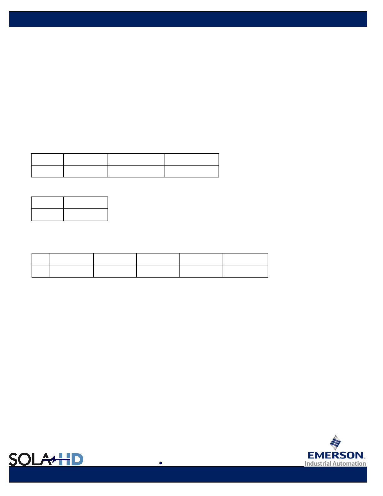
1. Model Number
Model No. Model Supported Interface Bus Description
73-546-001 SHP Series USB USB to I²C Module for SHP Case
Technical Reference Note
73-544-001 SHP Series CAN/RS485 CAN/RS485 to I²C Module for SHP Case
73-544-002 SHP Series CAN/RS485 CAN/RS485 to I²C Module for SHP Case
Options
None
www.solahd.com solahd.technicalservices@emerson.com

Technical Reference Note
2. General Description
73-546-001
This module is for SHP USB to I²C adapter module that connects to a standard USB port (see Figure 4) found on most
compatible for any IBM PCs and provides bi-directional communication with I²C devices using the I²C protocol. The
adapter is powered directly from the SHP case internal power supply 5VSB and PC’s USB port. The on-board LED
illuminates after the USB host has successfully enumerated it.
Figure 1. SHP USB to I²C Adapter
73-544-001
This module is for SHP CAN/RS485 to I²C adapter module that connects to CAN bus through CaseRx/CaseTx found on
SHP cases output connector (see Figure 5) and communicates to I²C Bus using Modbus Protocol for RS485 Bus and
Modified Modbus for CANbus. The adapter is powered directly from the SHP case internal power supply 5VSB. The onboard LED illuminates after the CAN/RS485 host has successfully enumerated it.
Figure 2. SHP CAN/RS485 to I²C Adapter
73-544-002
This module is for SHP CAN/RS485 to I²C adapter that connects to CAN bus through CaseRx/CaseTx found on SHP
cases output connector (see Figure 6) and communicates to I²C Bus using Modbus Protocol for RS485 Bus and Modified
Modbus for CAN bus. The adapter is powered directly from the SHP case internal power supply 5VSB.
Figure 3. SHP CAN/RS485 to I²C Adapter
www.solahd.com solahd.technicalservices@emerson.com

Technical Reference Note
3. Electrical Specifications
Absolute Maximum Ratings
Stress in excess of those listed in the “Absolute Maximum Ratings” may cause permanent damage to the power supply.
These are stress ratings only and functional operation of the unit is not implied at these or any other conditions above
those given in the operational sections of this TRN. Exposure to any absolute maximum rated condition for extended
periods may adversely affect the power supply’s reliability.
Parameter
Model Symbol Min Typ Max Unit
Input Voltage
Internal Supply +5Vsb Standby
Maximum Output Power
Ambient Operating Temperature
Storage Temperature
Humidity (non-condensing)
Non-operating
Altitude
Non-operating
Operating
Operating
All models V
All models P
All models T
All models T
4.75 - 5.25 Vdc
CC
O,max
0 - +40
A
STG
-20 - +50 ºC
All models
All models
20
10
All models
All models
Table 1. Absolute Maximum Ratings
- - 2.5 W
-
-
-
-
-
-
90
95
10,000
30,000
ºC
%
%
feet
feet
www.solahd.com solahd.technicalservices@emerson.com

Technical Reference Note
Hardware Signal Definition
Name of Signal: A0, A1, A2
Description: Pins that determine the address of the adapter.
Source of Input or
Destination of output:
Physical Implementation: A0, A1, A2 is connected to RA0, RA1, RA2 of the microcontroller and is connected to
Valid Range, Accuracy,
and/or Tolerance:
Timing: N/A
Name of Signal: SCL, SDA
Description: These pins are the clock and data pins of the I²C.
Source of Input or
Destination of output:
Physical Implementation: Connected to the header.
Valid Range, Accuracy,
and/or Tolerance:
Timing: I²C Frequency: 10 to 100kHz
By default the adapter address is 111, but if connected to the PSU, the address could
be changed through the header.
Vcc and to the header.
High or Low
PSU I²C (when connected to the header).
High or Low
Name of Signal: UART_TX, UART_RX
Description: transmit and receive pins of UART
Source of Input or
Destination of output:
Physical Implementation: RC6 and RC7 connected to DI, and RO pins of the RS485 transceiver.
Valid Range, Accuracy,
and/or Tolerance:
Timing: 1.2kbps to 115.2 kbps
www.solahd.com solahd.technicalservices@emerson.com
Other systems connected to the header.
High or Low

Technical Reference Note
Name of Signal: CAN_TX, CAN_RX
Description: Transmit and receive pins of CAN
Source of Input or
Destination of output:
Physical Implementation: RB2 and RB3 connected to RXD and TXD pins of the CAN transceiver.
Valid Range, Accuracy,
and/or Tolerance:
Timing: 125kbps to 500kbps
Name of Signal: LED
Description: pin that controls the LED output
Source of Input or
Destination of output:
Physical Implementation: RB5 connected to transistor.
Valid Range, Accuracy,
and/or Tolerance:
Timing: N/A
Function Summary
Function Description Sub-Function
CAN communication CAN transmit CAN_TX Refer to software requirements
Other systems connected to the header.
High or Low
output controlled by microcontroller.
High or Low
Referenced Signals Remarks
Description
CAN receive CAN_RX Refer to software requirements
UART communication UART transmit UART_TX Refer to software requirements
UART receive UART_RX Refer to software requirements
I²C communication I²C send SDA, SCL Refer to software requirements
I²C receive SDA, SCL Refer to software requirements
Control LED
(for 73-546-001 only)
N/A LED Should be ON when the unit is powered on.
Blinking fast when an error is received.
www.solahd.com solahd.technicalservices@emerson.com

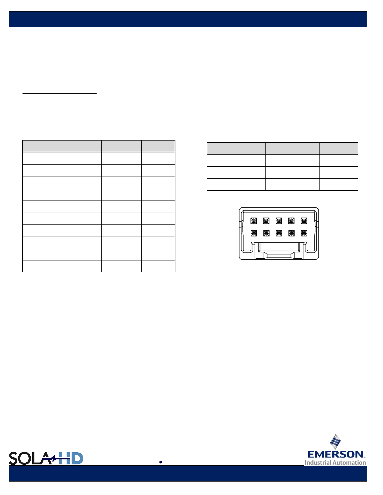
4. Mechanical Specificat io n
Connector Definition
73-546-001
Standard Mini-B USB to I²C Interface.
Description Pin Name Pin No.
Bus Supply Voltage VBUS 1
USB Data Low DATA - 2
USB Data High DATA + 3
USB ID ID 4
Bus Supply Return GND 5
Technical Reference Note
Connector Type Part No. Vendor
Output 54819-0572 Molex
Mate 88732-8600 Molex
73-544-001
SHP CAN/RS485 to I²C Interface.
Description Pin Name Pin No.
No Connection N/C 1
CAN Bus L / RS485 A CASE RX 2
CAN Bus H / RS485 B CASE TX 3
Serial Clock Signal SCL 4
Serial Data Signal SDA 5
Address Bit 0 A0 6
Address Bit 1 A1 7
Address Bit 2 A2 8
Bus Supply Return COMMON 9
5V System Bus 5VCC 10
Figure 4. Connector Mini-USB
Connector Type Part No. Vendor
Output CI4405M1HR0 Molex
Mate CI4405S0000 Molex
10 6
5 1
Figure 5. Connector J2
www.solahd.com solahd.technicalservices@emerson.com
Connector Definition
73-544-002
SHP CAN/RS485 to I²C Interface.
Technical Reference Note
Description Pin Name Pin No.
No Connection N/C 1
CAN Bus L / RS485 A CASE RX 3
CAN Bus H / RS485 B CASE TX 5
Serial Clock Signal SCL 7
Serial Data Signal SDA 9
Address Bit 0 A0 2
Address Bit 1 A1 4
Address Bit 2 A2 6
Bus Supply Return COMMON 8
5V System Bus 5VCC 10
Connector Type Part No. Vendor
Output 5016451020 Molex
Mate 5016461000 Molex
Terminal Pin 5016471000 Molex
1 9
2 10
Figure 6. Connector J2
www.solahd.com solahd.technicalservices@emerson.com

Weight
The 73-544-001 weight is 4.2 grams maximum.
The 73-544-002 weight is 3.8 grams maximum.
The 73-546-001 weight is 5.1 grams maximum.
Technical Reference Note
www.solahd.com solahd.technicalservices@emerson.com
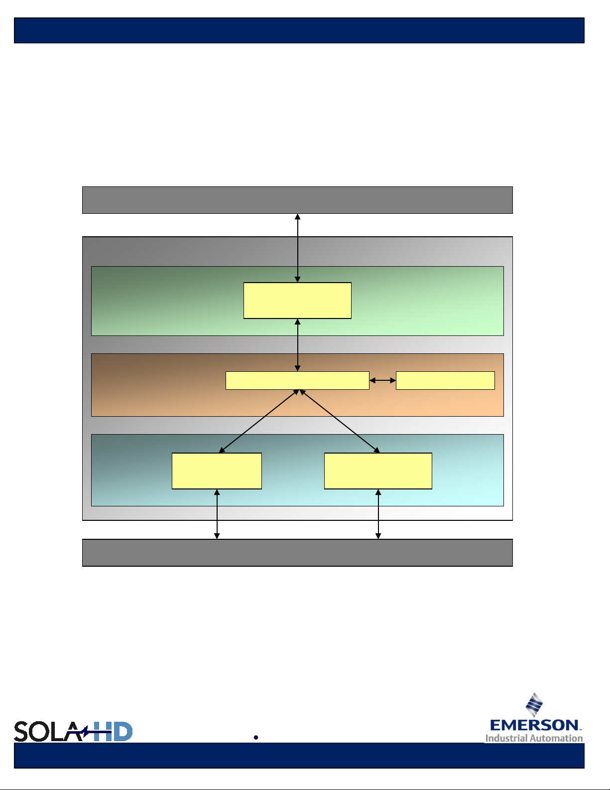
5. Hardware Interfaces
See below system overview for 73-544-001/73-544-002.
Slave/Server Device(s)
Technical Reference Note
Adapter
Output Protocols
Adapter Protocol
I²C with SMBus
Support
Adapter Command
Adapter Controls
Input Protocols
RS485 using
Modbus
CAN using
Modified Modbus
Master/Client Device(s)
Figure 7. RS485/CAN-to-I²C Over view
www.solahd.com solahd.technicalservices@emerson.com
Technical Reference Note
6. Software Interfaces
This specification defines the software design specification for the extension board adapter – for interfacing the SHP and
SHP Series to CAN Bus and RS485 Bus. The extension board has microcontroller to convert I²C data lines to CAN Bus
and RS485 Bus data lines.
6.1 Adapter Protocol Overview
The RS485/CAN-to-I²C uses 2 Input Protocols and 1 Output Protocol.
Protocol Type Command Index
The Master/Client Device(s) initiate communication to the target Slave/Server Device(s) by choosing an available and
supported Input Protocol of the Adapter (RS485 or CAN). The Master/Client sends an Adapter Command Packet to the
Adapter Command Control using the chosen Input Protocol.
The Adapter Command Packet contains the Command Code needed for the Adapter to know which command the
Master/Client requests. The Adapter Command Control decodes the requested command and performs it. If the
command requested requires data transfer to a target Slave/Server through I²C, the Adapter Command Decoder passes
the parameter to the Output Protocol. The Output Protocol then performs the transaction, and if successful – it transfers
the resulting Output, if any, to the Adapter Command Control.
After performing the requested command, the Adapter Command Control then creates an Adapter Response Packet. The
Adapter Response Packet contains Error Codes in determining the success of the command execution, and resulting
output, if any. The Adapter Command Control then sends the Adapter Response Packet to the Master/Client through the
same Input Protocol used in transferring the Adapter Command Packet.
If the Master/Client sends another transaction while the adapter is still processing the previous command, it will send a
busy signal reply to the Master/Client.
Input RS485 using Modbus 0x01
Input CAN using modified Modbus 0x02
Output I²C with SMBus support 0x80
Table 2. Adapter Protocol
6.2 Protocol Transaction
The Adapter Protocol defines the data packet sent by the Master/Client Device(s) to make the Adapter send data to the
target Slave/Server Device(s) or control adapter functions. Master/Client Device(s) to Adapter transaction starts with the
Master/Client Device(s) sending the Adapter an Adapter Command Packet, which is composed of the Command Code
and its Parameters. If the Adapter successfully receives the Adapter Command Packet, the Adapter will perform the
command requested. Upon completion of the command, the Adapter will respond by sending an Adapter Response
Packet to the Master/Client Device(s) containing the Command Code, Error Code (to determine a successful completion
or not), and other parameters requested. Figure 8 illustrates this transaction.
www.solahd.com solahd.technicalservices@emerson.com

Technical Reference Note
Figure 8. Adapter Protocol
6.3 Adapter Command and Response Packets
The Command Packet, as shown in Table 3, is composed of 2 Bytes of Command Code and optional 64 Bytes Parameter.
The 1st Byte of the Command Code is the Command Index, which serves as grouping for the Adapter Commands, and
the 2nd Byte is the Command Function, which specifies the function needed under the group indicated in the 1st Byte.
The 2 Byte Command Code is then followed by optional Parameter Bytes. The length and content of the Parameter
Bytes (if any) depends on the command requested and is included in the definition of the Command. The Command
Parameters can have a size of up to 64 Bytes.
The Response Packet data frame, as shown in Table 4, is composed of 2 Bytes of Command Code, a 1 Byte Error Code,
and optional 64 Bytes Output. The 2 Bytes of Command Code is the same Command Code received by the Adapter in
the Adapter Command Packet. The 3rd Byte is the Error Code, which is used to determine if the command execution
succeeds, or what type of error occurred. The Error Code is then followed by optional Command Output Bytes, provided
that the Error Code returns no error. Depending on the error that occurred, there may be no Command Output. The
length and content of the Command Output Bytes (if any) depends on the command requested and is included in the
definition of the Command. The Command Output can have a size of up to 64 Bytes.
Byte 1
Command Index
Byte 2
Command Function
Table 3. Command Packet
Byte 3 to 66
Command Parameters
Byte 1
Command Index
www.solahd.com solahd.technicalservices@emerson.com
Byte 2
Command Function
Table 4. Response Packet
Byte 3
Error Code
Byte 4 to 67
Command Output

Technical Reference Note
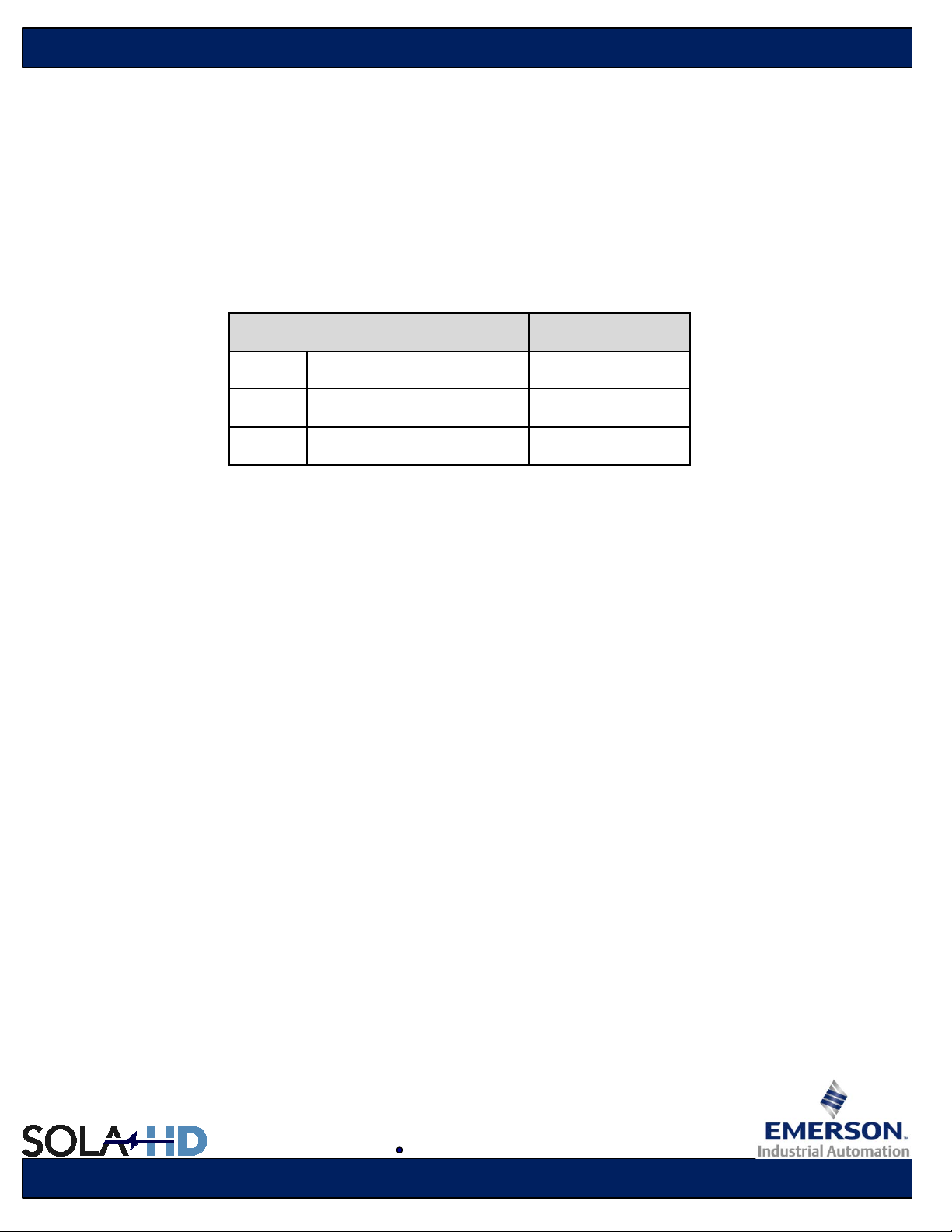
6.3.1 Command Index
The Command Index is used to group together the available functions into Command Types. Table 5 below shows the
summary and description of the Command Index grouped in each Command Type.
Adapter Control handles Functions for general Adapter Control. This includes: Adapter reset, Digital Output control
(such as LED), Digital Input reading, etc. Adapter Control also contains functions in controlling the Active Input and
Output Protocol, such as current Active Protocol reporting and switching. Command Index 0x00 is reserved for Adapter
Control Command Type.
Input Protocol Control handles Functions for controlling the available Input Protocols. This includes: Baud/Clock rate
control, Input Protocol Reset, etc. Command Index 0x01–0x7F is reserved for Input Protocol Control Command Type.
Output Protocol Control handles Functions for controlling the available Output Protocols. This includes: Baud/Clock rate
control, Output Protocol Enabling/Disabling, Output Protocol Reset, etc. This also contains the specific commands to be
able to send data using the specific Output Protocol, such as Reading and Writing data. Command Index 0x80–0xFF is
reserved for Output Protocol Control Command Type.
Command Index Command Type Description
0x00 Adapter Control Control adapter specific functions and
active input protocol control functions.
0x01 to 0x7F Input Protocol Control Controls input protocol specific functions.
0x01 – for RS485 using Modbus
0x02 – for CAN using modified Modbus
0x80 to 0xFF Output Protocol Control Controls output protocol specific functions
and sending data through the output
protocol.
0x80 - I²C with SMBus support
Table 5. Command Index Grouping
www.solahd.com solahd.technicalservices@emerson.com

Technical Reference Note
6.3.2 Error Code
The Error Code is returned in the Adapter Response Packet to determine if the Command requested from the Adapter
Command Packet is successful, or not. If not successful, the Error Code returned will help determine what error occurred.
For most Adapter Commands, Error Codes 0x00 to 0x04 are used. For these Error Codes, the Adapter Response Packet
will always return no Command Output. Error Codes 0x05 to 0xFF are reserved to be define by the specific Adapter
Command Function. Depending on the Command Function, Error Codes for this range may or may not return a
Command Output in the Adapter Response Packet (see specific Command Function description). Table 6 below
summarizes the Error Codes.
Error Code Error Type
The order by which Error Code are determined are as follows:
1. Checks if the Adapter Command Packet is received from the currently active Input Protocol. If the Adapter Command
Packet is received from and Inactive Input Protocol, Error Code 0x01 is returned.
2. Check if the Command Index is valid and supported. If the Command Index is not supported or invalid, then Error
Code 0x02 is returned.
3. Check if the Command Function is valid and supported. If the Command Function is not supported or invalid, then
Error Code 0x03 is returned.
4. Check if the Command Parameter if valid and enough for the Command Function to execute. This includes too
many/less Command Parameter Bytes, Command Parameter given if none is needed, invalid format, and invalid range. If
the Command Parameter is not valid enough for the Command Function to execute, then Error Code 0x04 is returned.
Note that some invalid Command Parameter may still allow the Command Function to execute. During this case, an
Error Code of 0x05–0xFF is to be used. The Command Function definition is to clarify which cases of Invalid Command
Parameter will return an Error Code 0x04, as well as when will a different Error Code (if any) will be returned and the
corresponding response and Output.
0x00 No Error
0x01 Inactive Input Protocol
0x02 Inval id Command Index
0x03 Inval id Command Function
0x04 Inval id Command Parameter
0x05 Inactive Output Protocol
0x06-0xFF Command Function Defined
Table 6. Error Code Summary
5. The Command Function will then execute, and detect Function specific Errors (including some Invalid Command
Parameter described above). If any error is found, the corresponding 0x05–0xFF will be returned, along with the
corresponding Command Output (if any), as defined in the Command Function description. If no error is found after
Command Function execution, Error Code 0x00 is returned, along with the corresponding Command Output (if any), as
defined in the Command Function description.
www.solahd.com solahd.technicalservices@emerson.com
6.4 Adapter Control Commands
Table 7 shows the supported Adapter Control Functions.
Function Code Function Name Parameter Length
0x00 Adapter Version 0 3
0x02-0x0F Reserved --- --0x10 Get Active Input Protocol 0 1
0x11 Set Active Input Protocol 1 1
0x12-0x1F Reserved --- --0x20 Get Active Output Protocol 0 1
0x21 Set Active Output Protocol 1 1
0x22-0x1F Reserved --- --0xF0 Go into Bootloader Mode 0 --0xFF A dapter Reset 0 See Description
(Bytes)
Technical Reference Note
Output Length
(Bytes)
0x00 - Adapter Version
Parameter None
Description Returns current Adapter Firmware Version. The 3 Bytes returned are
Output Byte 1 – Adapter Firmware Major Version.
Additional Error Codes 0x05 – Not Applicable, None Output Protocol Function.
Table 7. Adapter Control Commands
the Adapter Firmware Major, Minor and Test Version in decimal format.
i.e. An Adapter Firmware with version 01.02.56 will return the following
(in hex):
Byte 1 – 0x01
Byte 2 – 0x02
Byte 3 – 0x38
Byte 2 – Adapter Firmware Minor Version.
Byte 3 – Adapter Firmware Test Version.
www.solahd.com solahd.technicalservices@emerson.com

Active Input Protocol Collision. Current Active Input Protocol will
0x10 – Get Acti ve Input Protocol
Technical Reference Note
0x11 – Set Active Input Protocol
Parameter None
Description Returns 1 Byte of data containing the Command Index of the currently
Output Byte 1 – Current Active Input Protocol (0x01–0x7F).
Additional Error Codes 0x01 – Not applicable, see Description.
Parameter Byte 1 – Command Index of Input Protocol to set as Active
Description Sets the Active Input Protocol to the Input Protocol of the Command
Active Input Protocol. If there is no Active Input Protocol, a 0x00 will be
returned as Output.
This Function should be available even on an Inactive Input Protocol,
but should not cause that Input Protocol to be Active. Thus, Error Code
0x01 is ignored for this Function.
See Section 6.5 for details on how Active Input Protocol is determined.
0x05 – Not Applicable, None Output Protocol Function.
(0x00, 0x01–0x7F).
Index provided in the Parameter. Command Index provided must be
within valid range and supported, or a 0x00 (None) for the function to
execute, or an Invalid Command Parameter will occur. The current
Active Input Protocol must also be Idle (i.e. not in the middle of a
transaction) for it to be changed, otherwise, an Active Input Protocol
Collision Error (0x06) will occur. On an Active Input Protocol Collision,
the current Active Input Protocol will not be changed and will be
returned as the Output.
This Function should be available even on Inactive Input Protocol; thus,
Error Code 0x01 is ignored on this Function.
See Section 6.5 for details on how Active Input Protocol is determined.
Output Byte 1 – Actual Active Input Protocol set (0x00, 0x01–0x7F).
Additional Error Codes 0x01 – Not applicable, see Description.
0x04 – Will not respond if Input Protocol given is outside of valid range
(0x00, 0x01–0x7F), or not supported.
0x05 – Not Applicable, None Output Protocol Function.
www.solahd.com solahd.technicalservices@emerson.com
0x06 –
not change, and will be returned as Output.

0x20 – Get Acti ve Output Protocol
Technical Reference Note
0x21 – Set Active Output Protocol
Parameter None
Description Returns 1 Byte of data containing the Command Index of the currently
Output Byte 1 – Current Active Output Protocol (0x80–0xFF).
Additional Error Codes 0x05 – Not Applicable, None Output Protocol Function.
Parameter Byte 1 – Command Index of Output Protocol to set as Active
Description Sets the Active Output Protocol to the Output Protocol of the Command
Output Byte 1 – Actual Active Output Protocol set (0x00, 0x80–0xFF).
Additional Error Codes 0x04 – Will not respond if Output Protocol given is outside of valid
Active Output Protocol. If there is no Active Output Protocol, a 0x00 will
be returned as Output.
See Section 6.8 for details on how Active Output Protocol is
determined.
(0x00, 0x80–0xFF).
Index provided in the Parameter. Command Index provided must be
within valid range and supported, or a 0x00 (None) for the function to
execute, or an Invalid Command Parameter will occur. The current
Active Output Protocol must also be Idle (i.e. not in the middle of a
transaction) for it to be changed, otherwise, an Active Output Protocol
Collision Error (0x06) will occur. On an Active Output Protocol
Collision, the current Active Output Protocol will not be changed and
will be returned as the Output.
See Section 6.8 for details on how Active Output Protocol is
determined.
range (0x00, 0x80–0xFF), or not supported.
0x05 – Not Applicable, None Output Protocol Function.
0x06 – Active Output Protocol Collision. Current Active Output Protocol
will not change, and will be returned as Output.
0xF0 – Go into Bootloader Mode
Parameter None
Description It writes to the jump key that the adapter needs to go to bootloader
Output None
Additional Error Codes None
www.solahd.com solahd.technicalservices@emerson.com
mode. And resets the microcontroller. It then restarts and goes into
bootloader mode.

0xFF – Adapter Reset
Technical Reference Note
Parameter None
Description Performs software reset for the Adapter. This resets buffers and
settings to default used by all Input, Adapter and Output Protocols.
Since performing reset will not make returning of the Adapter Response
Packet possible, the Master/Client should not request for Adapter
Response Packet. The Master/Client should perform necessary
profile/configuration clearing on its side if needed.
Output See Description
Additional Error Codes See Description
www.solahd.com solahd.technicalservices@emerson.com

Technical Reference Note
6.5 Active Input Protocol
Only one Input Protocol at a given instance can perform transfer of Adapter Command/Response Packets to the Adapter
Protocol. The Input Protocol allowed for transfer is called the Active Input Protocol.
Upon initialization of the Adapter, the Active Input Protocol is set to None, flagged as 0x00 when checked using the Get
Active Input Protocol function. Each Input Protocol that is available and ready for will then continuously listen/wait for
transfer from the Master/Client. Once any of the Input Protocol received a successful transaction from the Master/Client
(as defined on particular Input Parameter), the Adapter Protocol will then set that Input Protocol as the Active Input
protocol. Once an Input Protocol becomes Active, any successful transaction from the other present Input Protocol will
return an Inactive Input Protocol Error with few exceptions. The Active Input Protocol will remain as the Active Input
Protocol until any of the following happens:
• No successful transaction occurs (idle) on the Active Input Protocol for at least 10 seconds. In this case, the Active
Input Protocol will be go to None (0x00).
• An Adapter Reset function is commanded. In this case, the Active Input Protocol will be re–initialized and returned to
None (0x00).
• A Set Active Input Protocol command was commanded and successfully (No Error, 0x00) performed. In this case, the
Active Input Protocol is set to the new Input Protocol set in the Parameter.
A specific Function under the Command Index of the Input Protocol causes change in Active Input Protocol. New Active
Input Protocol will depend on the definition of the Function.
6.6 Input Protocol – RS485 using Modbus (0x01)
Input Protocol 0x01 is assigned to the RS485 bus using the Modbus protocol. RTU (Remote Terminal Unit) mode is used
for Modbus.
• Data are sent per byte and should not have more than 1.5 characters between each byte.
• If more than 3.5 characters spacing between next byte is achieved, the next byte is considered the next packet.
6.6.1 Server Address
Adapter Server Address when using this Input Protocol is determined by 3 Address Bits to set the Server Address. Table
8 below shows the summary of the Address Bit Logic vs. Adapter Server Address.
Server Address A2 A1 A0
0x30 (0b00110000) 0 0 0
0x32 (0b00110010) 0 0 1
0x34 (0b00110100) 0 1 0
0x36 (0b00110110) 0 1 1
0x38 (0b00111000) 1 0 0
0x3A (0b00111010) 1 0 1
0x3C (0b00111100) 1 1 0
0x3E (0b00111110) 1 1 1
Table 8. Modbus Server Address Summary
www.solahd.com solahd.technicalservices@emerson.com

Technical Reference Note
6.6.2 Adapter Command/Response Packet Holding Registers
Holding registers 0x0000–0x003F are assigned to the Adapter Command Packets, and 0x0040–0x007F stores is
assigned for the Adapter Response Packet. Note that each holding register holds 2 Bytes. In counting the Byte order, the
MSB comes first, followed by the LSB. The mapping will then be: in 0x0000 of the holding register MSB will be Byte 1 of
the Adapter Command Packet, 0x0000 LSB will be Byte 2, 0x0001 MSB will be Byte 3, 0x0001 LSB will be Byte 4 and so
on; 0x0030 of the holding register MSB will be Byte 1 of the Adapter Response Packet, 0x0030 LSB will be Byte 2,
0x0031 MSB will be Byte 3, 0x0031 LSB will be Byte 4 and so on. Figure 9 below shows an illustration of the holding
register mapping.
This Input Protocol will use the Modbus functions Read Holding Registers (0x03), Write Multiple Registers (0x10), and
Read/Write Multiple Registers (0x17) to transfer the Adapter Command/Response Packet. The Write Multiple Registers
is used to write the Adapter Command Packet (0x0000–0x002F). The Read Holding Registers is used to read the
Adapter Response Packet (0x0030–0x005F). The Read/Write Multiple Registers can be used to perform a Write of the
Adapter Command Packet followed by a Read of the Adapter Response Packet sequence. Writing and reading to the
Holding Register always starts in the first byte.
0x0000
0x0001
…
0x002F
0x0030
0x0031
…
0x005F
Byte 1 Byte 2
Byte 3 Byte 4
… …
Adapter Command
Packet Bytes
Byte 95 Byte 96
Byte 1 Byte 2
Byte 3 Byte 4
… …
Adapter Response
Packet Bytes
Byte 95 Byte 96
Figure 9. Modbus Holding Register Mapping
www.solahd.com solahd.technicalservices@emerson.com

6.6.2.1 Supported Modbus Functions
0x03 Read Holding Register:
Request
Function Code 1 Byte 0x03
Starting Address 2 Bytes 0x0030–0x005F
Quantity of Registers 2 Bytes 1–64
Response
Function Code 1 Byte 0x03
Byte Count 1 Byte 1–128
Register Value 1–128 Bytes
Adapter Response Packet
Technical Reference Note
0x10 Write Multiple Registers:
Request
Function Code 1 Byte 0x10
Starting Address 2 Bytes 0x0000–0x002F
Quantity of Registers 2 Bytes 1–64
Byte Count 1 Bytes 1–128
Register Value 1–128 Bytes
Response
Function Code 1 Byte 0x10
Starting Address 2 Bytes 0x0030–0x005F
Quantity of Registers 2 Bytes 1–64
Address Command Packet
www.solahd.com solahd.technicalservices@emerson.com

0x17 Read/Write Multiple Registers:
Request
Function Code 1 Byte 0x17
Read Starting Address
Quantity to Read 2 Bytes 1–64
Write Starting Address
Quantity of Write 2 Bytes 1–64
Write Byte Count 1 Bytes 1–128
Write Registers Value
2 Bytes 0x0030–0x005F
2 Bytes 0x0000–0x002F
1–128 Bytes
Address Command Packet
Technical Reference Note
Response
Function Code 1 Byte 0x17
Byte Count 1 Byte 1–128
Read Registers Value
1–128 Bytes
Adapter Response Packet
www.solahd.com solahd.technicalservices@emerson.com

Technical Reference Note
6.6.3 Input Protocol Control Functions
Table 10 below shows the supported Functions for Input Protocol RS485 using Modbus.
0x00 – Input Protocol Description
Function
Code
0x00
0x01 Get EUSART Baud Rate 0 1
0x02 Set EUSART Baud Rate 1 1
0x09 Get Read/Write Timeout 0 1
0x0A Set Read/Write Timeout 1 1
0xFF Input Protocol Reset 0 See Description
Parameter None
Description Returns a string of characters that will describe the Input
Output Byte 1–0x52 (R)
Input Protocol Description
Table 10. Supported RS485 using Modbus Functions
Protocol assigned in the Command Index. The data will be
in ASCII format, with a New Line character (‘\n’, 0x0A) at
the end. Bytes beyond the New Line will be padded with
0xFF.
Byte 2–0x53 (S)
Byte 3–0x34 (4)
Byte 4–0x38 (8)
Byte 5–0x35 (5)
Byte 6–0x20 ( )
Byte 7–0x75 (u)
Byte 8–0x73 (s)
Byte 9–0x69 (i)
Byte 10–0x6E (n)
Byte 11–0x67 (g)
Byte 12–0x20 ( )
Byte 13–0x4D (M)
Byte 14–0x6F (o)
Byte 15–0x64 (d)
Byte 16–0x62 (b)
Byte 17–0x75 (u)
Byte 18–0x73 (s)
Byte 19–0x0A (\n)
Byte 20–64–0xFF (pad)
Function Name
Parameter
Length (Bytes)
0 64
Output Length
(Bytes)
Additional
Error Codes
www.solahd.com solahd.technicalservices@emerson.com
0x05 – Not Applicable, None Output Protocol Function.

0x01 – Get EUSART Baud Rate
Technical Reference Note
0x02 – Set EUSART Baud Rate
Parameter None
Description Returns the current 1 Byte code for EUSART Baud.
Possible Outputs will be:
0x01–0.3 Kbps
0x02–1.2 Kbps
0x03–2.4 Kbps
0x04–9.6 Kbps
0x05–19.2 Kbps
0x06–57.6 Kbps
0x07–115.2 Kbps
Output Byte 1 – Code for current EUSART Baud Rate.
Additional
Error Codes
Parameter Byte 1 – Code for desired EUSART Baud Rate.
Description Sets current EUSART Baud Rate to the Desired EUSART Baud Rate in
Output Byte 1 – Code for current EUSART Baud Rate.
Additional
Error Codes
None.
the parameter.
Sending 0x00 will enable the Auto-Baud Detection.
Possible Parameters will be:
0x00–Auto-detect
0x01–0.3 Kbps
0x02–1.2 Kbps
0x03–2.4 Kbps
0x04–9.6 Kbps
0x05–19.2 Kbps
0x06–57.6 Kbps
0x07–115.2 Kbps
Other values will return an Invalid Parameter error (0x04).
Output will return the code of EUSART Baud Rate set.
0x04 – Will not respond if EUSART Baud Rate given is not of valid value
(see Description).
www.solahd.com solahd.technicalservices@emerson.com

0x09 – Get Read/Write Timeout
Technical Reference Note
0x0A – Set Read/Write Timeout
Parameter None
Description Returns the read timeout of RS485. (currently not used)
Possible Outputs will be:
0x01–100ms
0x02–200ms
:
:
0xFF–25.5s
Output Byte 1 – Actual Read Timeout set.
Additional
Error Codes
Parameter Byte 1 – time of read timeout before error (0x01 – 0xFF)
Description Sets the read timeout of RS485. It is defaulted to 1 second if not set. It is
Output Byte 1 – Actual Read Timeout set.
Additional
Error Codes
None.
incremented per 100ms. (currently not used) i.e. If the desired read
timeout is 500ms, A value of 5 should be written in the parameter.
0x04 – Will not respond if Read timeout given is not of valid value
(see Description).
0xFF – Input Protocol Reset
Parameter None.
Description Performs software reset for the Input Protocol. This resets buffers and
settings to default used by all Input Protocol. Since performing reset will
not make returning of the Adapter Response Packet possible, the
Master/Client should not request for Adapter Response Packet. The
Master/Client should perform necessary profile/configuration clearing on
its side if needed.
Output See Description.
Additional
Error Codes
See Description.
www.solahd.com solahd.technicalservices@emerson.com
Technical Reference Note
6.6.4 RS485 Transaction Error
Defined here are the Error Codes that will be used by functions in this Input Protocol that involves RS485 transfer
(functions that refer in this in definition). See Table 11 below for Error Codes and description.
Error Code
0x50
Error Code
Read Timeout Error
Table 11. RS485 Transfer Error Code Summary
Commands
A timeout occurred when reading in the CAN bus.
www.solahd.com solahd.technicalservices@emerson.com

Technical Reference Note
6.7 Input Protocol – CAN using Modified Modbus (0x02)
Input Protocol 0x02 is assigned to the CAN bus using the as Modbus frame format, with modifications to take advantage
of CAN higher layer features. RTU (Remote Terminal Unit) format is also for Modbus. Changes are as follows:
• The Server Address will be placed in the Identifier, instead as the 1st Byte of the Modbus Frame. A Standard (11-bit)
Identifier will be used. Since Server Address is 8-bit, the last 3 bits (bits 8-10) of the Standard Identifier will be padded
with 0’s, and bits 0-7 will be the Server Address. Hence, the Modbus Frame will start with the Function Code.
• No Error Check Byte at the end of the Modbus Frame. The CRC checking in the CAN Frames will be used for data
integrity checking.
• Since CAN Data Frames can have a maximum of 8 Bytes, and Modbus Frames can exceed 8 Bytes, the Client is to
keep on sending the Modbus Frames in 8-Byte chunks. The CAN Input Protocol is to collect this chunk until a Data
Frame with 0 Bytes in the Control Field Data Length Code (DLC) is received from the Client. Once the 0 Byte DLC Data
Frame is received, the Modbus Frame will then be process and its function executed. The Client will then send a Remote
Frame (assuming Data Frame is received by Server successfully) to request receipt of the Modbus Response Frame
(which contains the Adapter Response Frame).
• The CAN Output Protocol will also send a Data Frame with 0 Bytes in the Control Field Data Length Code (DLC) to
signal the Client that the transmission is complete.
6.7.1 Server Address
Adapter Server Address when using this Input Protocol is determined by 3 Address Bits to set the Server Address. The
Address Bits is to be shared with that used by RS485 using Modbus Input Protocol. Hence, Modbus Server Address for
both RS485 and CAN will be the same. Table 12 below shows the summary of the Address Bit Logic vs. Adapter Server
Address. Note the 3-bit 0's pad on bits 8-10, as discussed in Section 6.7 above.
Server Address A2 A1 A0
0x30 (0b00000110000) 0 0 0
0x32 (0b00000110010) 0 0 1
0x34 (0b00000110100) 0 1 0
0x36 (0b00000110110) 0 1 1
0x38 (0b00000111000) 1 0 0
0x3A (0b00000111010) 1 0 1
0x3C (0b00000111100) 1 1 0
0x3E (0b00000111110) 1 1 1
Table 12. Modbus Server Address Summary
www.solahd.com solahd.technicalservices@emerson.com

Technical Reference Note
6.7.2 Adapter Command/Response Packet Holding Registers
Holding Register mapping for CAN using modified Modbus Input Protocol is the same that used for RS485 using Modbus
Input Protocol. Note that in MCU memory, the Holding Registers for CAN using modified Modbus Input Protocol is
separate with that used by RS485 using Modbus Input Protocol. Refer to section 6.6.2 for Holding Register mapping
details.
6.7.2.1 Supported Modbus Functions
CAN using modified Modbus Input Protocol supports the same Modbus Functions used for RS485 using Modbus Input
Protocol. Refer to section 6.6.2.1 for supported Modbus function details.
6.7.3 Input Protocol Control Functions
Table 13 below shows the supported Functions for Input Protocol CAN using modified Modbus.
Function
Function Name
Code
0x00 Input Protocol Description 0 64
0x01 Get CAN Baud Rate 0 1
0x02 Set CAN Baud Rate 1 1
0x09 Get Read Timeout 1 1
0x0A Set Read Timeout 1 1
0xFF Input Protocol Reset 0 See Description
Table 13. Supported CAN using modified Modbus
Parameter
Length (Bytes)
Output Length
(Bytes)
www.solahd.com solahd.technicalservices@emerson.com

0x00 – Input Protocol Description
Technical Reference Note
Parameter None
Returns a string of characters that will describe the Input Protocol
Description
Output
Additional
Error Codes
assigned in the Command Index. The data will be in ASCII format, with
a New Line character (‘\n’, 0x0A) at the end. Bytes beyond the New
Line will be padded with 0xFF.
Byte 1 - 0x43 (C)
Byte 2 - 0x41 (A)
Byte 3 - 0x4E (N)
Byte 4 - 0x20 ( )
Byte 5 - 0x75 (u)
Byte 6 - 0x73 (s)
Byte 7 - 0x69 (i)
Byte 8 - 0x6E (n)
Byte 9 - 0x67 (g)
Byte 10 - 0x20 ( )
Byte 11 - 0x6D (m)
Byte 12 - 0x6F (o)
Byte 13 - 0x64 (d)
Byte 14 - 0x69 (i)
Byte 15 - 0x66 (f)
Byte 16 - 0x69 (i)
Byte 17 - 0x65 (e)
Byte 18 - 0x64 (d)
Byte 19 - 0x20 ( )
Byte 20 - 0x4D (M)
Byte 21 - 0x6F (o)
Byte 22 - 0x64 (d)
Byte 23 - 0x62 (b)
Byte 24 - 0x75 (u)
Byte 25 - 0x73 (s)
Byte 26–0x0A (\n)
Byte 27–64–0xFF (pad)
0x05–Not Applicable, None Output Protocol Function.
www.solahd.com solahd.technicalservices@emerson.com

0x01 – Get CAN Baud Rate
Technical Reference Note
0x02 – Set CAN Baud Rate
Parameter None
Description
Output Byte 1 – Code for current CAN Baud Rate.
Additional
Error Codes
Parameter Byte 1 – Code for desired CAN Baud Rate.
Description
Output Byte 1 – Code for current CAN Baud Rate.
Additional
Error Codes
Returns the current 1 Byte code for CAN Baud.
Possible Outputs will be:
0x01 – 10 Kbps
0x02 – 20 Kbps
0x03 – 50 Kbps
0x04 – 125 Kbps
0x05 – 250 Kbps
0x06 – 500 Kbps
0x07 – 800 Kbps
0x08 – 1 Mbps
None.
Sets current CAN Baud Rate to the Desired CAN Baud Rate in the
parameter.
Possible Parameters will be:
0x01 – 10 Kbps
0x02 – 20 Kbps
0x03 – 50 Kbps
0x04 – 125 Kbps
0x05 – 250 Kbps
0x06 – 500 Kbps
0x07 – 800 Kbps
0x08 – 1 Mbps
Other values will return an Invalid Parameter error (0x04).
Output will return the code of CAN Baud Rate set.
0x04 – Will not respond if CAN Baud Rate given is not of valid value
(see Description).
0x09 – Get Read Timeout
Parameter None
Description Returns the read timeout of CAN.
Output Byte 1 – Actual Read Timeout set.
Additional
Error Codes
Possible Outputs will be:
0x01 – 100ms
0x02 – 200ms
:
:
0xFF – 25.5s
None.
www.solahd.com solahd.technicalservices@emerson.com
0x0A – Set Read Timeout
Technical Reference Note
0xFF – Input Protocol Reset
Parameter Byte 1 – time of read timeout before error (0x01 – 0xFF)
Description
Output Byte 1 – Actual Read Timeout set.
Additional
Error Codes
Parameter None.
Description
Output See Description.
Additional
Error Codes
Sets the read timeout of CAN. It is defaulted to 1 second if not set. It is
incremented per 100ms.
I.e. If the desired read timeout is 500ms, a value of 5 should be written in
the parameter.
0x04 – Will not respond if Read timeout given is not of valid value
(see Description).
Performs software reset for the Input Protocol. This resets buffers and
settings to default used by all Input Protocol. Since performing reset will
not make returning of the Adapter Response Packet possible, the
Master/Client should not request for Adapter Response Packet. The
Master/Client should perform necessary profile/configuration clearing on
its side if needed.
See Description.
6.7.4 CAN Transaction Error
Defined here are the Error Codes that will be used by functions in this Input Protocol that involves CAN transfer (functions
that refer in this in definition). See Table 14 below for Error Codes and description.
Error Code
0x60
Error Type Commands
Read Timeout
Error
Table 14. CAN Transfer Error Code Summary
A timeout occurred when reading in the CAN bus.
(DLC zero is not sent after read timeout is reached)
www.solahd.com solahd.technicalservices@emerson.com

Technical Reference Note
6.8 Active Output Protocol
For cases of multiple Output Protocols defined in the Adapter, only one Output Protocol at a given instance, can perform
transfer of Adapter Command/Response Packets to the Adapter Protocol. The Output Protocol allowed for transfer is
called the Active Output Protocol. Upon initialization of the Adapter, the Active Output Protocol is set to None, flagged as
0x00 when checked using the Get Active Output Protocol function (see Section 6.4). Once any of the Output Protocol has
performed a successful transaction to the Slave/Server (as defined on particular Output Parameter), the Adapter Protocol
will then set that Output Protocol as the Active Output protocol. Once an Output Protocol becomes Active, any
transaction request for Slave/Server using other present Output Protocol will return an Inactive Output Protocol Error (see
Section 6.3.2). The Active Output Protocol will remain as the Active Output Protocol until any of the following happens:
•No successful transaction occurs (idle) on the Active Output Protocol for at least 10 secs. In this case, the Active Output
Protocol will be go to None (0x00).
•An Adapter Reset function is commanded. In this case, the Active Output Protocol will be re–initialized and returned to
None (0x00).
•A Set Active Output Protocol command was commanded and successfully (No Error, 0x00) performed. In this case, the
Active Output Protocol is set to the new Output Protocol set in the Parameter. See Section 6.4.
A specific Function under the Command Index of the Output Protocol causes change in Active Output Protocol. New
Active Output Protocol will depend on the definition of the Function.
6.9 Output Protocol – I²C with SMBus Support (0x80)
Table 15 below shows the supported Functions for Output Protocol I²C with SMBus Support.
Function Code Function Name
0x00 Output Protocol Description 0 64
0x01 Get I²C Frequency 0 2
0x02 Set I²C Frequency 2 2
0x10 I²C Write Variable, 3–64 0
0x11 I²C Read 3 Variable, 1–64
0x20 SMBus Quick Command 1 0
0x21 SMBus Send Byte 3 0
0x22 SMBus Receive Byte 2 1
0x23 SMBus Write Byte/Word Variable, 5–6 0
0x24 SMBus Read Byte/Word 4 Variable, 1–2
0x25 SMBus Block Write Variable, 5–36 0
0x26 SMBus Block Read 3 Variable, 2–33
Parameter
Length
(Bytes)
Output
Length
(Bytes)
0x27 SMBus Process Call Variable, 5–36 Variable, 2–33
0xFF Output Protocol Reset 0 0
TABLE 15. Supported I²C with SMBus Output Protocol Functions
www.solahd.com solahd.technicalservices@emerson.com

0x00 – Output Protocol Description
Technical Reference Note
Parameter None
Returns a string of characters that will describe the Output Protocol
Description
Output
Additional Error
Codes
assigned in the Command Index. The data will be in ASCII format, with
a New Line character (‘\n’, 0x0A) at the end. Bytes beyond the New Line
will be padded with 0xFF.
Byte 1 – 0x49 (I)
Byte 2 – 0x32 (2)
Byte 3 – 0x43 (C)
Byte 4 – 0x20 ( )
Byte 5 – 0x75 (u)
Byte 6 – 0x73 (s)
Byte 7 – 0x69 (i)
Byte 8 – 0x6E (n)
Byte 9 – 0x67 (g)
Byte 10 – 0x20 ( )
Byte 11 – 0x53 (S)
Byte 12 – 0x4D (M)
Byte 13 – 0x42 (B)
Byte 15 – 0x75 (u)
Byte 16 – 0x73 (s)
Byte 17 – 0x0A (\n)
Byte 18 – 64–0xFF (pad)
None.
0x01 – Get I²C Frequency
Parameter None
Description
Output
Additional Error
Codes
Returns the current 2 Bytes for I²C SCL frequency in KHz set in the
configuration.
Possible Output is from 10 KHz to 400 KHz. Default value is 100 KHz.
Returned frequency accuracy is guaranteed only for frequencies from
10 KHz–100 KHz to be within 2%. Accuracy above 100 KHz is not
guaranteed.
I.e. I²C SCL frequency of 100 KHz will return:
Byte 1–0x64.
Byte 2–0x00.
Byte 1 – I²C SCL frequency LSB.
Byte 2 – I²C SCL frequency MSB.
I²C SCL frequency is in KHz and is of Unsigned data format.
None.
www.solahd.com solahd.technicalservices@emerson.com

0x02 – Set I²C Frequency
Technical Reference Note
0x10 – I²C Write
Byte 1 – Desired I²C SCL frequency LSB.
Parameter
Description
Output
Additional Error
Codes
Parameter
Description
Output None.
Additional Error
Codes
Byte 2 – Desired I²C SCL frequency MSB.
Desired I²C SCL frequency is in KHz and is of Unsigned data format.
Sets current I²C SCL frequency to the Desired I²C SCL frequency in the
parameter. Accepted Parameter is from 10 KHz to 400 KHz. Values
outside if this range will result in and Invalid Parameter Error (0x04).
While I²C SCL frequency of up to 400 KHz is accepted, actual I²C SCL
frequency accuracy is only guaranteed up to 2% at 10 KHz–400 KHz.
Accuracy at I²C SCL frequency of above 100 KHz is no guaranteed. I²C
communication at I²C SCL frequency of above 100 KHz is also not
guaranteed.
Output will return the I²C SCL frequency set.
Byte 1 – I²C SCL frequency (in KHz) LSB.
Byte 2 – I²C SCL frequency (in KHz) MSB.
0x04 – Will not respond if I²C SCL frequency given is outside of valid
range (10 KHz–400 KHz).
Byte 1 – I²C Address.
Byte 2 – Include Stop Bit.
Byte 3 – Number of Data Bytes to write.
Byte 4 – 64-Data Bytes to write.
I²C Address uses 7-bit Addressing.
Include Stop Bit is of Boolean data type.
Number of Data Bytes is of Unsigned data format.
Sends a Number of Data Bytes as stated in the parameter to the
provided I²C Address. The I²C Address uses 7-bit addressing. In the I²C
addressing, the 8th bit is not included in the addressing (masked).
Number of Data Bytes accepted is from 0–61. Requesting to send a
Number of Data Bytes outside of this range will result in an Invalid
Parameter (0x04) error. The number of Data Bytes provided must also
match the value of the Number of Data Bytes, or an Invalid Parameter
(0x04) error will occur. Number of Data Bytes can be 0, in this case,
there must be no data after Byte 3.
The Data Bytes to be written (if any) will be taken from Bytes 4-64. Byte
4 will be sent 1
written.
Byte 2 will be interpreted as a Boolean data type, and will be used to
determine if a Stop Bit is sent at the end of writing. A Boolean value of
TRUE will cause the Stop Bit to be sent, and a value of FALSE will not.
0x04 – Will not respond if the Number of Data Bytes given is outside of
valid range (0-64); or number of Data Bytes provided does match with
the provided Number of Data Bytes to write.
Refer to Section 6.9.2 for I²C Transaction Errors.
st
, followed by Byte 5, and so forth, until all Data Bytes is
www.solahd.com solahd.technicalservices@emerson.com

0x11 – I²C Read
Technical Reference Note
Parameter
Description
Output Byte 1-64 – Data Bytes read.
Additional Error
Codes
Byte 1 – I²C Address.
Byte 2 – Include Stop Bit.
Byte 3 – Number of Data Bytes to read.
I²C Address uses 7-bit Addressing.
Include Stop Bit is of Boolean data type.
Number of Data Bytes is of Unsigned data format.
Reads a Number of Data Bytes as stated in the parameter to the
provided I²C Address. In the I²C addressing, the 8th bit is not included
in the addressing (masked).
Number of Data Bytes accepted is from 1–64. Requesting to read data
outside of this range will result in an Invalid Parameter (0x04) error.
The Data Bytes received will be placed at Bytes 1–64 of the Output. 1
nd
Data Byte read is placed to Byte 1, 2
Data Byte received to Byte 2,
and so forth, until a number of Data Byte equal to the Number of Data
Bytes is read.
Byte 2 will be interpreted as a Boolean data type, and will be used to
determine if a Stop Bit is sent send at the end of writing. A Boolean
value of TRUE will cause the Stop Bit to be sent, and a value of
FALSE will not.
0x04 – Will not respond if the Number of Data Bytes given is outside of
valid range (1–64).
Refer to Section 6.9.2 for I²C Transaction Errors.
st
0x20 – SMBus Quick Command
Parameter Byte 1 – I²C Address.
Description Performs a Quick Command, as defined in the SMBus protocol, to the
Output None.
Additional Error
Codes
I²C Address uses 7-bit Addressing.
provided I²C Address. In the I²C addressing, the 8th bit is not included
in the addressing (masked).
Refer to Section 6.9.2 for I²C Transaction Errors.
www.solahd.com solahd.technicalservices@emerson.com

0x21 – SMBus Send Byte
Technical Reference Note
0x22 – SMBus Receive Byte
Parameter Byte 1 – I²C Address.
Description Performs a Send Byte, as defined in the SMBus protocol, to the
Output None.
Additional Error
Codes
Parameter Byte 1 – I²C Address.
Description Performs a Receive Byte, as defined in the SMBus protocol, to the
Output Byte 1 – Data Byte Received.
Additional Error
Codes
Byte 2 – Data Byte to send.
Byte 3 – PEC Enable.
I²C Address uses 7-bit Addressing.
PEC Enable is of Boolean data type.
provided I²C Address. In the I²C addressing, the 8th bit is not included
in the addressing (masked). The Data Byte to send is in Byte 2.
Byte 3 flags if PEC will be placed at the end of the packet (TRUE) or not
(FALSE).
Refer to Section 6.9.2 for I²C Transaction Errors.
Byte 2 – PEC Enable.
I²C Address uses 7-bit Addressing.
PEC Enable is of Boolean data type.
provided I²C Address. In the I²C addressing, the 8th bit is not included
in the addressing (masked).
Byte 3 flags if PEC of the received packet will be checked (TRUE) or not
(FALSE).
The Data Byte read is placed at Byte 1 of the Output.
Refer to Section 6.9.2 for I²C Transaction Errors.
www.solahd.com solahd.technicalservices@emerson.com

0x23 – SMBus Write Byte/Word
Technical Reference Note
Parameter Byte 1 – I²C Address.
Byte 2 – Command Code.
Byte 3 – Number of Data Bytes to write.
Byte 4 – PEC Enable.
For Write Byte:
Byte 5 – Data Byte to write.
For Write Word:
Byte 5 – Data Word to write LSB.
Byte 6 – Data Word to write MSB.
I²C Address uses 7-bit Addressing.
Number of Data Bytes is of Unsigned data format.
PEC Enable is of Boolean data type.
Description
Output None.
Additional Error
Codes
Performs a Write Byte/Word, as defined in the SMBus protocol, to the
provided I²C Address. In the I²C addressing, the 8th bit is not included in
the addressing (masked).
Byte 2 contains Command Code to be used. Byte 3 defines the Number of
Data Bytes to be written. Number of Data Bytes to be written can only be a
value of 1 (for Write Byte) or 2 (for Write Word), otherwise an Invalid
Parameter (0x04) error will occur.
The Data Bytes to be written will be taken from Bytes 5–6. For Write Byte,
Byte 5 will contain the Data Byte, and there must be no Byte 6. For Write
Word, Byte 5 will contain the LSB of the Data Word, and Byte 6 will
contain the MSB. Non–conformance will result in an Invalid Parameter
(0x04) error.
Byte 4 flags if PEC will be placed at the end of the packet (TRUE) or not
(FALSE).
0x04 – Will not respond if the Number of Data Bytes given is outside of
valid range (1–2); or number of Data Bytes provided does match with the
provided Number of Data Bytes to write.
Refer to Section 6.9.2 for I²C Transaction Errors.
www.solahd.com solahd.technicalservices@emerson.com

0x24 – SMBus Read Byte/Word
Technical Reference Note
Parameter Byte 1 – I²C Address.
Byte 2 – Command Code.
Byte 3 – Number of Data Bytes to read.
Byte 4 – PEC Enable.
I²C Address uses 7-bit Addressing.
Number of Data Bytes is of Unsigned data format.
PEC Enable is of Boolean data type.
Description Performs a Read Byte/Word, as defined in the SMBus protocol, to the
provided I²C Address. In the I²C addressing, the 8th bit is not included in
the addressing (masked).
Byte 2 contains Command Code to be used. Byte 3 defines the Number of
Data Bytes to be read. Number of Data Bytes to be read can only be a
value of 1 (for Read Byte) or 2 (for Read Word), otherwise an Invalid
Parameter (0x04) error will occur.
Byte 4 flags if the PEC of the read packet will be checked (TRUE) or not
(FALSE).
The Data Bytes read will be placed to Bytes 5–6. For Read Byte, the
Data Byte will be placed to Byte 5 and there will be no Byte 6. For Write
Word, the LSB of the Data Word will be placed to Byte 5, and the MSB
will be placed to Byte 6.
Output For Read Byte:
Byte 1 – Data Byte read.
For Read Word:
Byte 1 – Data Word read LSB.
Byte 2 – Data Word read MSB.
Additional Error
Codes
0x04 – Will not respond if the Number of Data Bytes given is outside of
valid range (1–2).
Refer to Section 6.9.2 for I²C Transaction Errors.
www.solahd.com solahd.technicalservices@emerson.com

0x25 – SMBus Block Write
Technical Reference Note
Parameter Byte 1 – I²C Address.
Description Performs a Block Write, as defined in the SMBus protocol, to the provided I²C Address. In
Output None.
Additional Error
Codes
0x26 – SMBus Block Read
Byte 2 – Command Code.
Byte 3 – Number of Data Bytes to write.
Byte 4 – PEC Enable.
Byte 5 – 36–Data Bytes to be written.
I²C Address uses 7-bit Addressing.
Number of Data Bytes is of Unsigned data format.
PEC Enable is of Boolean data type.
the I²C addressing, the 8th bit is not included in the addressing (masked).
Byte 2 contains Command Code to be used. Byte 3 defines the Number of Data Bytes to be
written. Number of Data Bytes to be written can be a value from 1–32, otherwise an Invalid
Parameter (0x04) error will occur. The number of the Data Bytes provided must also match
the value of the Number of Data Bytes, or an Invalid Parameter (0x04) error will occur.
st
The Data Bytes to be written will be taken from Bytes 5–36. Byte 5 will be sent 1
, followed
by Byte 6, and so forth, until all Data Bytes is written.
Byte 4 flags if PEC will be placed at the end of the packet (TRUE) or not (FALSE).
0x04 – Will not respond if the Number of Data Bytes given is outside of valid range (1–32);
or number of Data Bytes provided does match with the provided Number of Data Bytes to
write.
Refer to Section 6.9.2 for I²C Transaction Errors.
Parameter Byte 1 – I²C Address.
Byte 2 – Command Code.
Byte 3 – Data bytes to read
Byte 4 – PEC Enable.
I²C Address uses 7-bit Addressing.
Number of Data Bytes is of Unsigned data format.
Description Performs a Block Read, as defined in the SMBus protocol, to the provided I²C Address. In
PEC Enable is of Boolean data type.
the I²C addressing, the 8th bit is not included in the addressing (masked).
Byte 2 contains Command Code to be used.
Byte 3 flags if the PEC of the read packet will be checked (TRUE) or not (FALSE).
The Number of Data Bytes read will be placed to Byte 1 of the Output. The Data Bytes read
st
will be placed at Bytes 2–33 of the Output. 1
Data Byte read is placed to Byte 1, 2nd Data
Byte received to Byte 2, and so forth, until a number of Data Byte equal to the Number of
Data Bytes is read.
Output Byte 1 – Number of Data Bytes read.
Byte 2 – 33 Data Bytes read.
Additional Error
Refer to Section 6.9.2 for I²C Transaction Errors.
Codes
www.solahd.com solahd.technicalservices@emerson.com

0x27 – SMBus Process Call
Technical Reference Note
Parameter Byte 1 – I²C Address.
Byte 2 – Command Code.
Byte 3 – Number of Data Bytes to write.
Byte 4 – PEC Enable.
Byte 5 – 36 Data Bytes to write.
I²C Address uses 7-bit Addressing.
Number of Data Bytes is of Unsigned data format.
PEC Enable is of Boolean data type.
Description
Output Byte 1 – Number of Data Bytes read.
Additional Error
Codes
Performs a Process Call, as defined in the SMBus protocol, to the provided I²C
Address. In the I²C addressing, the 8th bit is not included in the addressing
(masked).
Byte 2 contains Command Code to be used. Byte 3 defines the Number of Data
Bytes to be written. Number of Data Bytes to be written can be a value from 1–
31, otherwise an Invalid Parameter (0x04) error will occur. The number of the
Data Bytes provided must also match the value of the Number of Data Bytes, or
an Invalid Parameter (0x04) error will occur.
The Data Bytes to be written will be taken from Bytes 5–36. Byte 5 will be sent
1st, followed by Byte 6, and so forth, until all Data Bytes is written.
Byte 4 flags if PEC will be placed at the end of the sent packet (TRUE) or not
(FALSE). It also flags if the PEC of the read packet will be checked (TRUE) or not
(FALSE).
The Number of Data Bytes read will be placed to Byte 1 of the Output. The Data
Bytes read will be placed at Bytes 2–33 of the Output. 1st Data Byte read is
placed to Byte 1, 2nd Data Byte received to Byte 2, and so forth, until a number of
Data Byte equal to the Number of Data Bytes is read.
Byte 2 – 33 Data Bytes read.
0x04 – Will not respond if the Number of Data Bytes given is outside of valid
range (1–31); or number of Data Bytes provided does match with the provided
Number of Data Bytes to write.
Refer to Section 6.9.2 for I²C Transaction Errors.
www.solahd.com solahd.technicalservices@emerson.com

0xFF – Output Protocol Reset
Technical Reference Note
Parameter None.
Description Performs software reset for the I²C Module. Clears all TX and RX
buffers, and resets I²C SCL clock to 100 KHz.
Output None.
Additional
Error Codes
None.
6.9.2 I²C Transaction Error
Defined here are the Error Codes that will be used by functions in this Output Protocol that involves I²C transfer (functions
that refer in this in definition). See Table 16 below for Error Codes and description.
Error Code Error Type Commands
0x10 Address NACK NACK occurred when Slave Address was Written to I²C bus.
0x11 Data NACK NACK occurred when Slave Address was Written to I²C bus.
0x20
0x21
Bus Collision
Write Collision
I²C Bus in use when Start or Stop bit was being sent.
I²C Bus in use when doing I²C Write.
0x31
0x32 Start Timeout Timeout occurred when waiting for sending of Start bit to finish
0x33 Restart Timeout Timeout occurred when waiting for sending of Restart bit to finish
0x34 Stop Timeout Timeout occurred when waiting for sending of Stop bit to finish
0x35 Read Timeout Timeout occurred when waiting for Read to I²C bus to finish
0x36
0x40
0x41
Idle Timeout Timeout occurred when waiting for I²C bus to be idle.
ACK Timeout Timeout occurred when waiting for sending of ACK to finish
Buffer Limit (Hardware buffer)
CRC Error CRC computation is not equal to the PEC sent
Table 16. I²C Transfer Error Code Summary
MCU Hardware Buffer flags overflow
www.solahd.com solahd.technicalservices@emerson.com

Technical Reference Note
7. Interface Protocol – Controller Area Network (CAN)
7.1 Command / Response Packet
Byte 1
Command Index
Byte 1
Command Index
Byte 2
Command Function
Command Packet
Byte 2
Command Function
Response Packet
Byte 3
Error Code
Byte 3 to 66
Command Parameters
Byte 4 to 67
Command Output
www.solahd.com solahd.technicalservices@emerson.com
Technical Reference Note
7.2 Adapter Protocol Commands
Using Command Index – Adapter Control (0x00).
ADAPTER VERSION (0x00)
This command returns current Adapter Firmware Version. The 3 bytes returned are the Adapter Firmware Major, Minor,
and Test Version in decimal format.
Example for CAN:
Send command (in Hex):
CAN ID Data Length Command Index Command code
Then, send command:
3E 2 00 00
CAN ID Data Length
Since CAN is 8-bytes data transmission, data length 0 must be send to indicate end of transmission.
Reply (in Decimal):
Output:
The data is interpreted in hexadecimal as version “01.00.00”
Byte 4 – 0x01
Byte 5 – 0x00
Byte 6 – 0x00
In reply, Data Byte 1 and Data Byte 2 returned the command index and command code in decimal form while Data
Byte 3 indicate error code and it should return 0 which pertains “No Error”, or else a transaction error occurred.
3E 0
ID Data Length Data Byte 1 Data Byte 2 Data Byte 3 Data Byte 4 Data Byte 5 Data Byte 6
6 2 0 0 0 1 0 0
www.solahd.com solahd.technicalservices@emerson.com
Technical Reference Note
7.3 Input Protocol Control Commands
Using Command Index - CAN Modified Modbus (0x02).
INPUT PROTOCOL DESCRIPTION (0x00)
This command returns a string of characters that will describe the Input Protocol assigned in the command index.
The data will be in ASCII format, with a new line character (‘\n’, 0x0A) at the end. Bytes beyond the new line
will be padded with 0xFF.
Example for CAN:
Send command (in Hex):
CAN ID Data Length Command Index Command code
Then, send command:
3E 2 02 00
CAN ID Data Length
Since CAN is 8-bytes data transmission, data length 0 must be send to indicate end of transmission.
Reply (in Decimal):
1
2nd 8-data byte
3
3E 0
ID Data Length Data
Byte 1
1 8 2 0 0 67 65 78 32 117
st
8-data byte
ID Data Length Data
Byte 1
1 8 115 105 110 103 32 109 111 100
ID Data Length Data
Byte 1
1 8 105 102 105 101 100 32 77 111
rd
8-data byte
Data
Byte 2
Data
Byte 2
Data
Byte 2
Data
Byte 3
Data
Byte 3
Data
Byte 3
Data
Byte 4
Data
Byte 4
Data
Byte 4
Data
Byte 5
Data
Byte 5
Data
Byte 5
Data
Byte 6
Data
Byte 6
Data
Byte 6
Data
Byte 7
Data
Byte 7
Data
Byte 7
Data
Byte 8
Data
Byte 8
Data
Byte 8
ID Data Length Data
1 8 100 98 117 115 10 255 255 255
th
4
8-data byte
Byte 1
www.solahd.com solahd.technicalservices@emerson.com
Data
Byte 2
Data
Byte 3
Data
Byte 4
Data
Byte 5
Data
Byte 6
Data
Byte 7
Data
Byte 8
Technical Reference Note
Output:
Converting Data Byte 4 (67d) of 1st set of 8 data byte up to Data Byte 4 of the 4th set of 8 data byte to its ASCII
equivalent, the result will be a string of “CAN using modified Modbus”. Succeeding byte will be 255d (FFh).
GET CAN BAUD RATE (0x01)
This command will return the current 1 byte code for CAN Baud rate. The command code for Adapter version for CAN
and RS485 Adapter is 0x01.
Example for CAN:
Send command (in Hex):
CAN ID Data Length Command Index Command code
Then, send command:
3E 2 02 01
CAN ID Data Length
3E 0
Since CAN is 8-bytes data transmission, data length 0 must be send to indicate end of transmission.
Reply (in Decimal):
ID Data Length Data Byte 1 Data Byte 2 Data Byte 3 Data Byte 4
1 4 2 1 0 4
Output:
CAN Adapter Baud rate is 125 Kbps.
Possible Outputs are: (in hex)
0x01 – 10 Kbps
0x02 – 20 Kbps
0x03 – 50 Kbps
0x04 – 125 Kbps
0x05 – 250 Kbps
0x06 – 500 Kbps
0x07 – 800 Kbps
0x08 – 1 Mbps
www.solahd.com solahd.technicalservices@emerson.com

Technical Reference Note
7.4 Output Protocol Control Commands
Using Command Index – I²C with SMBus support (0x80).
OUTPUT PROTOCOL DESCRIPTION (0x00)
This command returns a string of characters that will describe the Output Protocol assigned in the command index. The
data will be in ASCII format, with a new line character (‘\n’, 0x0A) at the end. Bytes beyond the new line will be padded
with 0xFF.
Example for CAN:
Send command (in Hex):
CAN ID Data Length Command Index Command code
Then, send command:
3E 2 80 00
CAN ID Data Length
3E 0
Since CAN is 8-bytes data transmission, data length 0 must be send to indicate end of transmission.
Reply (in Decimal):
ID Data Length Data
1 8 128 0 0 73 50 67 32 117
st
1
8-data byte
ID Data Length Data
1 8 115 105 110 103 32 83 77 66
2nd 8-data byte
ID Data Length Data
1 8 117 115 10 0 255 255 255 255
rd
3
8-data byte
Output:
Converting Data Byte 4 (73d) of 1st set of 8 data bytes up to Data Byte 2 of the 3rd set of 8 data byte to its ASCII
Byte 1
Byte 1
Byte 1
Data
Byte 2
Data
Byte 2
Data
Byte 2
Data
Byte 3
Data
Byte 3
Data
Byte 3
Data
Byte 4
Data
Byte 4
Data
Byte 4
Data
Byte 5
Data
Byte 5
Data
Byte 5
Data
Byte 6
Data
Byte 6
Data
Byte 6
Data
Byte 7
Data
Byte 7
Data
Byte 7
Data
Byte 8
Data
Byte 8
Data
Byte 8
equivalent, the result will be “I²C using SMBus”. Succeeding byte will be 255d (FFh).
www.solahd.com solahd.technicalservices@emerson.com

Technical Reference Note
GET I²C FREQUENCY (0x01)
This command will return the current 2 bytes I²C SCL frequency in kHz set in the configuration. Possible output is from
10kHz to 400kHz. Default value is 100kHz. Returned frequency accuracy is guaranteed only for frequencies from 10kHz100kHz to be within 2%. Accuracy above 100kHz is not guaranteed.
Example for CAN:
Send command (in Hex):
CAN ID Data Length Command Index Command code
Then, send command:
3E 2 80 01
CAN ID Data Length
3E 0
Since CAN is 8-bytes data transmission, data length 0 must be send to indicate end of transmission.
Reply (in Decimal):
ID Data Length Data
1 8 128 1 0 100 0
Output:
The default I²C frequency of the Adapter is 100kHz. Data Byte 4 is the I²C SCL frequency LSB and Data Byte 5 is the
I²C SCL frequency MSB. I²C SCL frequency is in kHz and is have unsigned data format.
Byte 1
Data
Byte 2
Data
Byte 3
Data
Byte 4
Data
Byte 5
www.solahd.com solahd.technicalservices@emerson.com

Technical Reference Note
I²C WRITE (0x10) AND READ (0x11)
Reads a Number of Data Bytes as stated in the parameter to the provided I²C Address. In the I²C addressing, the 8th bit
is not included in the addressing (masked). Number of Data Bytes accepted is from 1–64. Requesting to read data
outside of this range will result in an Invalid Parameter (0x04) error.
nd
The Data Bytes received will be placed at Bytes 1–64 of the Output. 1st Data Byte read is placed to Byte 1, 2
received to Byte 2, and so forth, until a number of Data Byte equal to the Number of Data Bytes is read.
Byte 2 will be interpreted as a Boolean data type, and will be used to determine if a Stop Bit is sent send at the end of
writing. A Boolean value of TRUE will cause the Stop Bit to be sent, and a value of FALSE will not. I²C Read involves I²C
write to determine which location on the memory map you are going to read.
READ MODEL NUMBER (From EEPROM of Power Supply)
Example for CAN:
Send I²C Write command (in Hex):
CAN ID Data Length Command Index Command code Data
Byte 1
Data
Byte 2
Data
Byte 3
Byte 4
Data Byte
Data
Command Index for Output Protocol is 0x80 and Command Code for I²C Write is 0x10. Data Byte 1 indicates the I²C
address or the external EEPROM address (0xA0, 0xA1, 0xA2 floating), Data Byte 2 tells to include stop bit and Data
Byte 3 is the number of data bytes to write. Model Number is located at EEPROM offset 0x19-0x24 (12 bytes).
Data bytes 4-64 are the data bytes to write.
Then, send command:
Since CAN is 8-bytes data transmission, data length 0 must be send to indicate end of transmission.
Reply (in Decimal):
Output:
3E 6 80 10 AE 01 01 19
CAN ID Data Length
3E 0
ID Data Length Data
Byte 1
1 3 128 16 0
Data
Byte 2
Data
Byte 3
Data Byte 1 and 2 returned the command index and command code respectively and Data Byte 3 gives a value of 0
that indicates No error or successful write.
www.solahd.com solahd.technicalservices@emerson.com

Technical Reference Note
Send I²C Read command (in Hex):
CAN ID Data Length Command Index Command Code Data
3E 5 80 11 AE 01 0C
Byte 1
Then, send command:
CAN ID Data Length
3E 0
Since CAN is 8-bytes data transmission, data length 0 must be send to indicate end of transmission.
Reply (in Decimal):
Data
Byte 2
Data
Byte 3
CAN ID Data Length Data
1
1 8 128 17 0 55 51 45 53 56
st
8 data byte
CAN ID Data Length Data
2
1 8 48 45 48 48 48 49 73
nd
8 data byte
Byte 1
Byte 1
Data
Byte 2
Data
Byte 2
Data
Byte 3
Data
Byte 3
Data
Byte 4
Data
Byte 4
Data
Byte 5
Data
Byte 5
Data
Byte 6
Data
Byte 6
Data
Byte 7
Data
Byte 7
Data
Byte 8
Output:
Converting Data Byte 4 (55d) of 1st set of 8 data byte up to Data Byte 5 of the 2nd set of 8 data byte to its ASCII
equivalent, the result will be “73-580-0001I”.
www.solahd.com solahd.technicalservices@emerson.com

8. Interface Protocol – RS485
8.1 Command / Response Packet
Technical Reference Note
Byte 1
Command Index
Byte 1
Command Index
Byte 2
Command Function
Command Packet
Byte 2
Command Function
Response Packet
Byte 3
Error Code
Byte 3 to 66
Command Parameters
Byte 4 to 67
Command Output
www.solahd.com solahd.technicalservices@emerson.com

Technical Reference Note
8.2 Adapter Control Commands
Using Command Index - Adapter Control (0x00).
ADAPTER VERSION (0x00)
This command returns current Adapter Firmware Version. The 3 bytes returned are the Adapter Firmware Major, Minor,
and Test Version in decimal format.
Example for RS485:
Send command (in Hex):
Address Command Index Command Code
Reply (in Decimal):
3E 00 00
Decimal: 62,0,0,
Command
Output:
The data is interpreted in hexadecimal as version “01.00.00”
Byte 4 – 0x01
Byte 5 – 0x00
Byte 6 – 0x00
In reply, Data Byte 1 and Data Byte 2 returned the command index and command code in decimal form while Data
Byte 3 indicate error code and it should return 0 which pertains “No Error”, or else a transaction error occurred.
Index
Data
Byte 1
0 0 0 1 0 0
Command
Code
Data
Byte 2
Error
Code
Data
Byte 3
Read
Data
Data
Byte 4
Read
Data
Data
Byte 5
Read
Data
Data
Byte 6
www.solahd.com solahd.technicalservices@emerson.com

Technical Reference Note
8.3 Input Protocol Control Commands
Using Command Index - RS485 using ModBus (0x01).
INPUT PROTOCOL DESCRIPTION (0x00)
This command returns a string of characters that will describe the Input Protocol assigned in the command index.
The data will be in ASCII format, with a new line character (‘\n’, 0x0A. 10d) at the end. Bytes beyond the new line
will be padded with 0xFF.
Example for RS485:
Send command (in Hex):
Address Command Index Command Code
3E 01 00
Decimal: 62,1,0,
Reply (in Decimal):
Data
Byte 1
1
2nd 8-data byte
3
4
1 0 0 82 83 52 56 53
st
8-data byte
Data
Byte 1
32 117 115 105 110 103 032 77
Data
Byte 1
111 100 98 117 115 10 255 255
rd
8-data byte
Data
Byte 1
255 255 255 255 255 255 255 255
th
8-data byte
Data
Byte 2
Data
Byte 2
Data
Byte 2
Data
Byte 2
Data
Byte 3
Data
Byte 3
Data
Byte 3
Data
Byte 3
Data
Byte 4
Data
Byte 4
Data
Byte 4
Data
Byte 4
Data
Byte 5
Data
Byte 5
Data
Byte 5
Data
Byte 5
Data
Byte 6
Data
Byte 6
Data
Byte 6
Data
Byte 6
Data
Byte 7
Data
Byte 7
Data
Byte 7
Data
Byte 7
Data
Byte 8
Data
Byte 8
Data
Byte 8
Data
Byte 8
Output:
Converting Data Byte 4 (82d) of 1st set of 8 data byte up to Data Byte 5 of the 3rd set of 8 data byte to its ASCII
equivalent, the result will be a string of “RS485 using Modbus”. Succeeding byte will be 255d (FFh).
www.solahd.com solahd.technicalservices@emerson.com
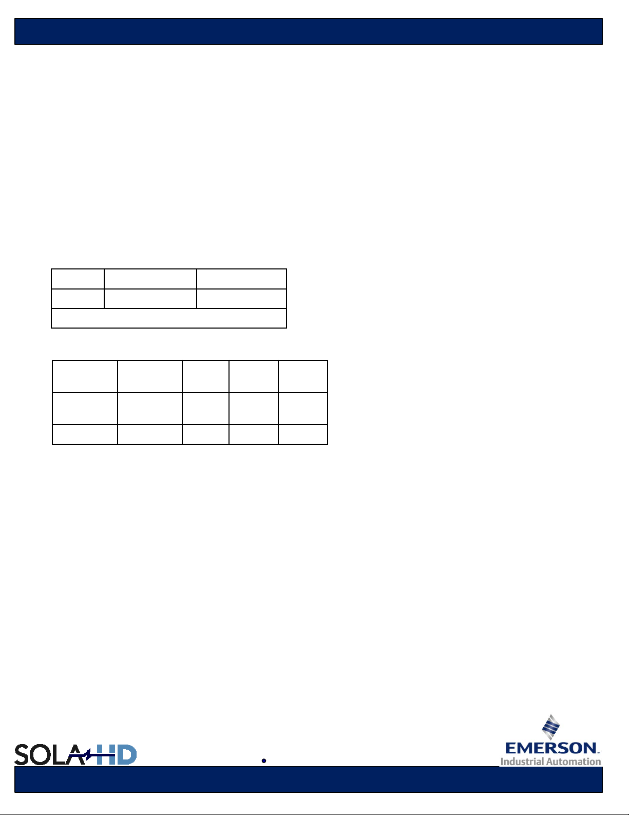
Technical Reference Note
GET CAN BAUD RATE (0x01)
This command will return the current 1 byte code for RS485 Baud rate. The command code for Adapter version for
RS485 Adapter is 0x01.
The Default RS485 Setting – Baud Rate: 9.6 kbps, Data: 8, Parity: None, Stop:1
Example for RS485:
Send command (in Hex):
Address Command Index Command Code
3E 01 01
Decimal: 62,1,1,
Reply (in Decimal):
Command
Output:
RS485 Adapter Baud rate is 9.6 Kbps.
Default Output is: (in hex)
0x04 – 9.6 Kbps
Index
Data
Byte 1
1 1 0 4 0
Command
Code
Data
Byte 2
Error
Code
Data
Byte 3
Read
Data
Data
Byte 4
Read
Data
Data
Byte 5
www.solahd.com solahd.technicalservices@emerson.com

Technical Reference Note
8.4 Output Protocol Control Commands
Using Command Index – I²C with SMBus Support (0x80).
OUTPUT PROTOCOL DESCRIPTION (0x00)
This command returns a string of characters that will describe the Output Protocol assigned in the command index. The
data will be in ASCII format, with a new line character (‘\n’, 0x0A, 10d) at the end. Bytes beyond the new line will be
padded with 0xFF.
Example for RS485:
Send command (in Hex):
Address Command Index Command Code
0x3E 0x80 0x00
Decimal: 62,128,0,
Reply (in Decimal):
Data
Byte 1
128 0 0 73 50 67 32 117
st
1
8-data byte
Data
Byte 1
115 105 110 103 32 83 77 66
2nd 8-data byte
Data
Byte 1
117 115 10 0 255 255 255 255
rd
3
8-data byte
Output:
Converting Data Byte 4 (73d) of 1st set of 8 data bytes up to Data Byte 2 of the 3rd set of 8 data byte to its ASCII
equivalent, the result will be “I²C using SMBus”. Succeeding byte will be 255d (FFh).
Data
Byte 2
Data
Byte 2
Data
Byte 2
Data
Byte 3
Data
Byte 3
Data
Byte 3
Data
Byte 4
Data
Byte 4
Data
Byte 4
Data
Byte 5
Data
Byte 5
Data
Byte 5
Data
Byte 6
Data
Byte 6
Data
Byte 6
Data
Byte 7
Data
Byte 7
Data
Byte 7
Data
Byte 8
Data
Byte 8
Data
Byte 8
www.solahd.com solahd.technicalservices@emerson.com

Technical Reference Note
GET I²C FREQUENCY (0x01)
This command will return the current 2 bytes I²C SCL frequency in kHz set in the configuration. Possible output is from
10kHz to 400kHz. Default value is 100kHz. Returned frequency accuracy is guaranteed only for frequencies from 10kHz100kHz to be within 2%. Accuracy above 100kHz is not guaranteed.
Example for RS485:
Send command (in Hex):
Address Command Index Command code
Reply (in Decimal):
3E 80 01
Decimal: 62,128,1
Data
Byte 1
128 1 0 100 0
Output:
The default I²C frequency of the Adapter is “100kHz”. Data Byte 4 is the I²C SCL frequency LSB and Data Byte 5 is
the I²C SCL frequency MSB. I²C SCL frequency is in kHz and is have unsigned data format.
Data
Byte 2
Data
Byte 3
Data
Byte 4
Data
Byte 5
www.solahd.com solahd.technicalservices@emerson.com

Technical Reference Note
I²C WRITE (0x10) AND READ (0x11)
Reads a Number of Data Bytes as stated in the parameter to the provided I²C Address. In the I²C addressing, the 8th bit
is not included in the addressing (masked). Number of Data Bytes accepted is from 1–64. Requesting to read data
outside of this range will result in an Invalid Parameter (0x04) error.
nd
The Data Bytes received will be placed at Bytes 1–64 of the Output. 1st Data Byte read is placed to Byte 1, 2
received to Byte 2, and so forth, until a number of Data Byte equal to the Number of Data Bytes is read.
Byte 2 will be interpreted as a Boolean data type, and will be used to determine if a Stop Bit is sent send at the end of
writing. A Boolean value of TRUE will cause the Stop Bit to be sent, and a value of FALSE will not. I²C Read involves I²C
write to determine which location on the memory map you are going to read.
READ MODEL NUMBER (From EEPROM of Power Supply)
Example for RS485:
Send I²C Write command (in Hex):
Address Command Index Command code Data
Byte 1
Data
Byte 2
Data
Byte 3
Data
Byte 4
Data Byte
Command Index for Output Protocol is 0x80 and Command Code for I²C Write is 0x10. Data Byte 1 indicates the I²C
address or the external EEPROM address (0xA0, 0xA1, 0xA2 floating), Data Byte 2 tells to include stop bit and Data
Byte 3 is the number of data bytes to write. Model Number is located at EEPROM offset 0x19-0x24 (12 bytes).
Data bytes 4-64 are the data bytes to write.
Reply (in Decimal):
Output:
Data Byte 1 and 2 returned the command index and command code respectively and Data Byte 3 gives a value of 0
that indicates No error or successful write.
3E 80 10 AE 1 1 19
62,128,16,174,1,1,25,
Data
Byte 1
128 16 0
Data
Byte 2
Data
Byte 3
www.solahd.com solahd.technicalservices@emerson.com

Send I²C Read command (in Hex):
Address Command Index Command Code Data
3E 80 11 AE 01 0C
62,128,17,174,1,12,
Byte 1
Data
Byte 2
Reply (in Decimal):
Data
Byte 1
128 17 0 51 55 45 53 56
st
1
8 data byte
Data
Byte 2
Data
Byte 3
Data
Byte 4
Data
Byte 5
Data
Byte 6
Byte 7
Data
Technical Reference Note
Data
Byte 3
Data
Byte 8
2
Data
Byte 1
48 45 48 48 48 49 73
nd
8 data byte
Data
Byte 2
Data
Byte 3
Data
Byte 4
Data
Byte 5
Data
Byte 6
Data
Byte 7
Output:
Converting Data Byte 4 (51d) of 1st set of 8 data byte up to Data Byte 7 of the 2nd set of 8 data byte to its ASCII
equivalent, the result will be “73-580-00001I”.
www.solahd.com solahd.technicalservices@emerson.com

Technical Reference Note
9. Interface Protocol – PMBus (For SHP Series Power Supplies)
9.1 Introduction
This SHP Protocol is compliant with the PMBus Power System Management Protocol Specification Part I Revision 1.0,
and the PMBus Power System Management Protocol Specification Part II Revision 1.0. Note that the PMBus is based on
the System Management Bus (SMBus) Specification. For supplementary information regarding the PMBus and SMBus
specifications, these documents will be referred to, and are considered part of this protocol:
Reference 1 PMBus™ Power System Management Protocol Specification, Part I
– General Requirements, Transport And Electrical Interface, Revision 1.0
www.powerSIG.org
Reference 2 PMBus™ Power System Management Protocol Specification, Part II
– Command Language, Revision 1.0
www.powerSIG.org
Reference 3 System Management Bus Specification, Revision 1.1
www.sbs-forum.org
Reference 4 System Management Bus (SMBus) Specification, Version 2.0
www.sbs-forum.org
9.2 SMBus Compliance
Packet Error Checking
Packet Error Checking (PEC) is optional in SMBus. The SHP secondary firmware version 2.06 or later supports PEC.
Ack/Nack
This version of the protocol does not issue a Nack in any case of errors above the data link layer. Communication
reliability can be achieved though read-back and/or through fault flags.
www.solahd.com solahd.technicalservices@emerson.com

Technical Reference Note
Bus Protocols
This protocol supports all SMBus bus protocols except the Quick Command and the Host Notify Protocol. Shown below
are excerpts from the System Management Bus (SMBus) Specification, Version 2.0 document for easy reference (figure
numbers are with reference to the said document).
www.solahd.com solahd.technicalservices@emerson.com

Technical Reference Note
www.solahd.com solahd.technicalservices@emerson.com

Technical Reference Note
www.solahd.com solahd.technicalservices@emerson.com
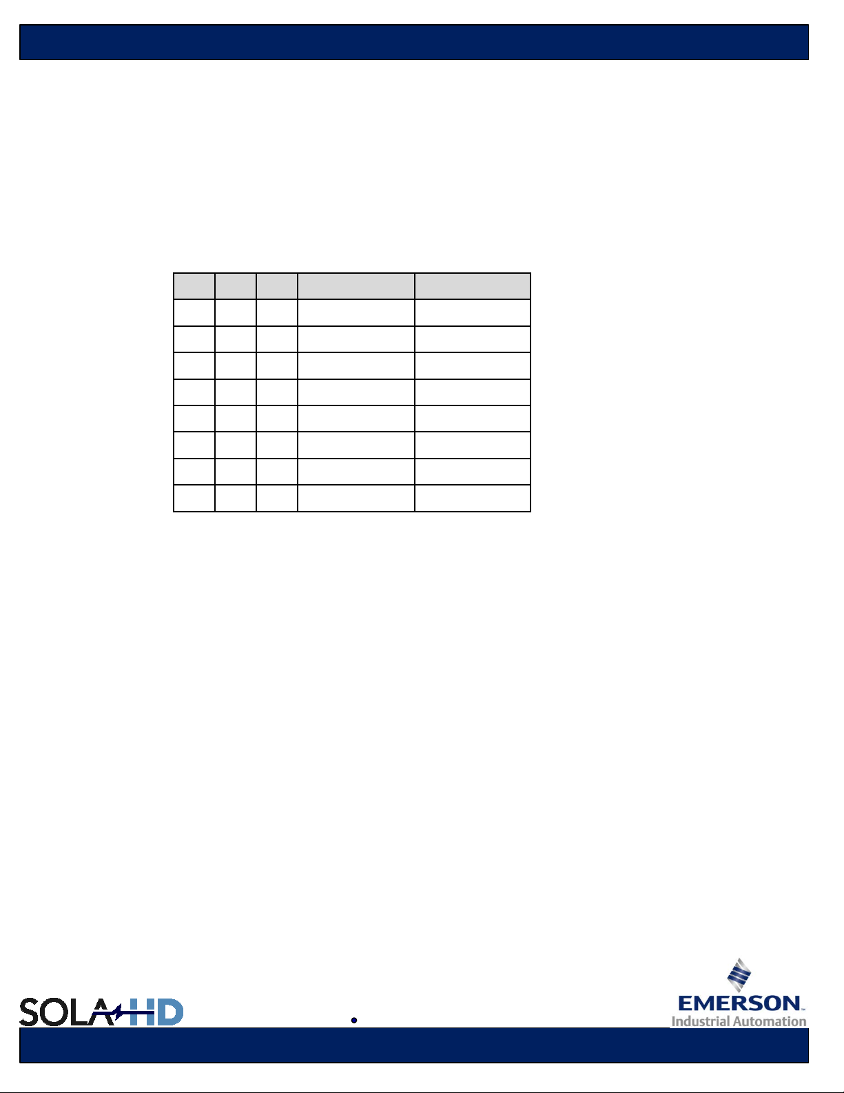
Technical Reference Note
Slave Device Addressing
This protocol’s addressing system is not dynamic, and is based only on the three input signals A0, A1, and A2.
The SHP valid addresses are:
A2 A1 A0 Write Address Read Address
0 0 0 30 31
0 0 1 32 33
This protocol also supports the General Call address (00h) for write operation only.
Optional SMBus Signals
This protocol does not use any of the Optional SMBus signals.
0 1 0 34 35
0 1 1 36 37
1 0 0 38 39
1 0 1 3A 3B
1 1 0 3C 3D
1 1 1 3E 3F
Table 22. SHP Device Addressing
www.solahd.com solahd.technicalservices@emerson.com
Technical Reference Note
INHIBIT_ENABLE_0
INHIBIT_ENABLE_1
9.3 PMBus Compliance
Command Error
This protocol does not support NACKing the command code or data bytes as they are being received. For any command
error, the CML fault bit in the STATUS_BYTE register is set. The STATUS_CML register is not supported however. To
see the detailed description of the fault, the CASE_FAULT_BYTE (Manufacturer Specific) register must be read. It
contains the Command Error and the Command Disabled flags which describes the kind of communication error
encountered.
Control Signal
The control signal in the SHP Power Supply unit is replaced by two signals, the INHIBIT_ENABLE_0 and the
INHIBIT_ENABLE_1 signals. The logic of these signals are controlled by the ON_OFF_CONFIG register bit1 (this bit is
originally the Control Pin Polarity flag, in this protocol however this is the Global Inhibit Flag). Depending on the value of
this bit, the logic of these signals are described below:
Parameter Reading
Due to the complexity of the internal communication system of the power supply, not all parameters that can be written is
readable. This is specially the case for commands targeted to an individual module, including the PMbus standard
commands TON_DELAY, VOUT_COMMAND, and IOUT_OC_FAULT_LIMIT. Since the Page register may change, the
previous parameter may not be applicable anymore.
Memory Model
There are four types of memory locations from which the configuration of the PSU can be defined. They are the
Operating Memory, the User Configuration Memory, the Factory Default Configuration Memory, and the Firmware Default
Configuration Memory locations.
0 0 Modules ON Modules OFF
0 1 Modules OFF Modules ON
1 0 Modules ON Modules OFF
1 1 Modules ON Modules OFF
Table 23. Control Signal
GLOBAL INHIBIT =
TRUE
GLOBAL INHIBIT =
FALSE
www.solahd.com solahd.technicalservices@emerson.com

Technical Reference Note
Operating Memory (R/W, Volatile)
The settings that are used by the PSU are stored in a volatile memory location called Operating Memory. This memory
location is the working memory of the PSU. Upon start-up, previously defined settings are loaded into the Operating
Memory from either of three nonvolatile memory locations (see succeeding items below). Configuration commands only
affect this memory area. Although the contents of this memory space are not saved at turnoff, they can be saved in either
the User or Factory Default Configuration Memory locations using the commands STORE_DEFAULT_ALL,
RESTORE_DEFAULT_ALL, STORE_USER_ALL, and RESTORE_USER_ALL.
User Configuration Memory (R/W, Non-volatile)
This memory location contains the main configuration setup that will be loaded at the Operating Memory every time the
PSU is powered. If any error is detected on this storage area, the User Configuration Error flag is set in the
CASE_FAULT_BYTE, and the CML fault bit in the STATUS_BYTE register is set. This memory location is non-volatile.
Factory Default Configuration Memory (R/W, Non-volatile)
This memory location contains the factory configuration setup that will only be loaded at the Operating Memory if an error
on the User Configuration Memory is detected upon power-up. If any error is detected on this storage area, the Default
Configuration Error flag is set in the CASE_FAULT_BYTE, and the CML fault bit in the STATUS_BYTE register is set.
This memory location is non-volatile.
Firmware Default Configuration Memory (Read-Only, Non-volatile)
This memory location is embedded on the firmware and is only loaded at the Operating Memory if both the User
Configuration Memory and the Default Configuration Memory encountered errors upon power-up. This memory location
is non-volatile.
Status Registers
This protocol will use only the STATUS_BYTE register. In conjunction with this, there is also a CASE_FAULT_BYTE
(Manufacturer Specific), a MODULE_COMMUNICATION_ERROR_BYTE (Manufacturer Specific), and a
CASE_STATUS_BYTE (Manufacturer Specific) register. Only the CASE_STATUS_BYTE register is real-time, since the
others requires the CLEAR_FAULTS command to reset the flags.
www.solahd.com solahd.technicalservices@emerson.com
Technical Reference Note
Data Formats
This protocol will use only the Direct Data Format for all parameters except for the Case Temperature related parameters,
which use a manufacturer-specific data format that has a resolution of 0.25 degrees Celsius. Refer to each parameter’s
associated commands for the details on the data format. Access to the coefficients is not supported as the data format is
fixed and already described in the specifications. This format is also applicable to the Output Voltage Related Parameters.
Shown below is an excerpt from the PMBus™ Power System Management Protocol Specification, Part II – Command
Language, Revision 1.0 document for easy reference (section numbers are with reference to the said document).
From Reference 2 - PMBus™ Power System Management Protocol Specification, Part II
Figure 9. Direct Data Format
www.solahd.com solahd.technicalservices@emerson.com

Technical Reference Note
9.4 Supported PMBus Standard Register
Listed below are the PMBus standard registers that are supported by the PSU. Details are described in the PMBus™
Power System Management Protocol Specification, Part II – Command Language, Revision 1.0 document, but excerpts
are shown for easy reference (table numbers are with reference to the said document).
STATUS_BYTE
This device uses the PMBus standard STATUS_BYTE register and all applicable flags. This register reflects all the
other faults such that:
a. Any Module Over Voltage Protection fault sets the STATUS_BYTE VOUT_OV Flag
b. Any Module Over Current Protection fault sets the STATUS_BYTE IOUT_OC Flag
c. Any Module Over Temperature Protection fault, Case Over Temperature Protection fault, Case Over
Temperature Protection warning, or Primary Over Temperature Protection warning, sets the STATUS_BYTE
TEMPERATURE Flag
d. Calling a Disabled Command, Command Errors, Fault in the Default or User Memory Locations, or errors in
any of the smart module internal UART communication buses, sets the STATUS_BYTE CML Flag
e. Any module UVP condition, module system fault, or an Over Power Limit Protection fault sets the
STATUS_BYTE OTHER Flag
f. The following commands will set the BUSY flag while the command operation is ongoing:
VOUT_COMMAND UVP_LIMIT_PERCENT
IOUT_OC_FAULT_LIMIT MODULE_OTP_LIMIT
TON_DELAY MODULE_CONFIG_FLAGS
EXTRACT_MODULE_VERSION LOAD_PREDEFINED_SETTING
EXTRACT_MODULE_CONFIG_BYTES MODULE_VSCALE_CALIBRATION
IOUT_SENSOR_CALIBRATION DIRECT_MODULE_ACCESS
OVP_LIMIT_PERCENT
g. The same commands in item f above will be temporarily disabled while the BUSY flag is set, along with these
commands:
READ_MODULE_VERSION
READ_MODULE_CONFIG_BYTES
READ_DIRECT_MODULE_ACCESS_REPLY
BIT STATUS BIT NAME DESCRIPTION
7 BUSY A fault was declared because the device was busy and unable to response.
6 OFF This bit is asserted if the unit is not providing power to the output, regardless of
the reason, including simply not being enabled.
5 VOUT_OV An output overvoltage fault has occurred.
4 IOUT_OC An output overcurrent fault has occurred.
3 VIN_UV An input undervoltage fault has occurred
2 TEMPERATURE A temperature fault or warning has occurred.
1 CML A communications, memory, or logic fault has occurred.
0 OTHER A fault or warning not listed in bits [7:1] has occurred.
Table 24. STATUS_BYTE Register
www.solahd.com solahd.technicalservices@emerson.com

Technical Reference Note
WRITE_PROTECT
This device uses the PMBus standard WRITE_PROTECT register and all applicable flags.
DATA BYTE VALUE DESCRIPTION
1000 0000 Disable all writes except to the WRITE_PROTECT command.
0100 0000 Disable all writes except to the WRITE_PROTECT, OPERATION, and PAGE commands.
0010 0000 Disable all writes except to the WRITE_PROTECT, OPERATION, and PAGE,
ON_OFF_CONFIG and VOUT_COMMAND commands.
0000 0000 Enable writes to all commands.
Table 25. WRITE_PROTECT Register
OPERATION
This device uses only bit 7 of the PMBus standard OPERATION register. The other flags are disregarded.
BITS [7:6] BITS [5:4] BITS [3:2] BITS [1:0]
00 XX XX XX Immediate Off
01 XX XX XX Soft Off
(With Sequencing)
10 00 XX XX On Off
10 01 01 XX On Mar gin Low
10 01 10 XX On Mar gin Low
10 10 01 XX On Margin High
Unit
On or Off
(No Sequencing)
Margin
State
N/A
N/A
(Ignore Fault)
(Act on Fault)
(Ignore Fault)
10 10 10 XX On Margin High
(Act on Fault)
Table 26. OPERATION Register
www.solahd.com solahd.technicalservices@emerson.com

Technical Reference Note
ON_OFF_CONFIG
This device uses the PMBus standard ON_OFF_CONFIG register and all applicable flags except for bit 0.
The Control Pin Polarity flag is used as the Global Inhibit flag instead.
BIT PURPOSE VALUE DESCRIPTION
[7:5] N/A Reserved for Future Use.
4 Sets the default to
either operate any
time power is present
or for the on/off to be
controlled by
CONTROL pin and
serial bus commands
0 Unit powers up any time power is present regardless of state of the
CONTROL pin.
1 Unit does not power up until commanded by the CONTROL pin and
OPERATION command (as programmed in bits [3:0].
3 Controls how the unit
responds to
commands received
via the serial bus
2 Controls how the unit
responds to the
CONTROL pin
1 Polarity of the
CONTROL pin
0 CONTROL pin action
when commanding the
unit to turn off
0 Unit ignores the on/off portion of the OPERATION command from the
serial bus
1 To start, the unit requires that the on/off portion of the OPERATION
command is instructing the unit to run.
0 Unit ignores the CONTROL pin (on/off controlled only the
OPERATION command).
1 Unit requires the CONTROL pin to be asserted to start the unit.
Depending on bit [3], the OPERATION command may also be
required to instruct the device to start before the output is energized.
0 Active low (Pull pin low to start the unit).
1 Active high (Pull pin high to start the unit).
0 Use the programmed turn off delay and fall time.
1 Turn off the output and stop transferring energy to the output as fast
as possible. The device’s product literature shall specify whether or
not the device sinks current to decrease the output voltage fall time.
Table 27. ON_OFF_CONFIG Register
www.solahd.com solahd.technicalservices@emerson.com

Technical Reference Note
9.5 Manufacturer Specific Register
PSU CONFIG
This register is stored in a non-volatile memory (User or Default Configuration Memory), and contains different
configuration flags that controls the fan speed, external EEPROM access, and start-up state.
BIT FLAG R/W DESCRIPTION
0 Fan Alarm Disabled R/W If this flag is set, fan fault detection is disabled (useful for PSU without fans).
1 Fan Off at Standby R/W At standby, fans operate at quiet mode by default. If this flag is set, the fans are turned off at
2 Fan Direction
Reversed Config
R/W Fan speed is based on the hottest temperature reading, and reaches the maximum at 50 degrees
3 Full Speed Override* R/W If this flag is set, fan speed is set to maximum.
4 Half Speed
Override*
5 Fan Voltage
Override*
6 FRU EEPROM Write
Enabled
7 Startup Operation
Mode On
R/W If this flag is set, fan PWM duty is set to half.
R Only If this flag is set, fan speed is set according to a requested fan voltage. This flag can be controlled
R/W
R/W If this flag is set, the initial value of the OPERATION register is set to ON mode
standby mode instead.
Celsius. If this flag is set, reverse fan air flow is assumed and fan speed
reaches the maximum at 40 degrees Celsius.
only by use of the VFAN_1 command.
If this flag is set, external write to the FRU EEPROM is allowed.
*These fan overrides work in conjunction with the default temperature-based fan control. Whichever results to the
highest fan speed will take control of the fans.
Table 28. PSU_CONFIG Register
ACTIVE SLOTS
This register contains the configuration of the module slots. The eight bits refer to the eight module slots. If a bit is
set, then the corresponding slot contains a module (smart or otherwise). This register is stored in a non-volatile
memory (User or Default Configuration Memory).
BIT
0 1
1 2
2 3
3 4
4 5
5 6
6 7
7* ---
MODULE
SLOT
POSITION
SH30, S3H3 SH45, S3H5
Figure 10. SHP Slot Configuration
*Unused bit.
www.solahd.com solahd.technicalservices@emerson.com

Technical Reference Note
SMART MODULES
This register contains the configuration of the smart modules. The eight bits refer to the eight module slots. If a bit is
set, then the corresponding slot contains a smart module. This register is stored in a non-volatile memory (User or
Default Configuration Memory).
BIT
0 1
1 2
2 3
3 4
4 5
5 6
6 7
7* ---
MODULE
SLOT
POSITION
SH30, S3H3 SH45, S3H5
Figure 10. SHP Slot Configuration
*Unused bit.
PSU_SETUP
This register contains flags regarding the current status of the PSU configuration access.
BIT FLAG R/W DESCRIPTION
0 Configuration Data
Status 0
1 Configuration Data
Status 1
2 Factory Setup Enabled R
R
Only
R
Only
These flags determine the state of the Operating Memory
11 - User Configuration Data was loaded
10 - Default Configuration Data was loaded
01 - Firmware Default Configuration Data was loaded
00 - Configuration Data in the Operating Memory was Updated
CONFIDENTIAL: This flag determine if the Factory Setup
Only
Commands are enabled.
Table 29. PSU_SETUP Register
www.solahd.com solahd.technicalservices@emerson.com

Technical Reference Note
CASE_STATUS_BYTE
This register contains flags about the current status of the PSU. Note that the flags here represents the real-time
status, and therefore does not require a separate command to be reset.
BIT FLAG R/W DESCRIPTION
0 Inhibit_Enable_0 R Only These flags mirrors the Control Signal Input state.
1 Inhibit_Enable_1 R Only
2 AC OK R Only This flag reflects the state of the AC input.
3 Bulk OK R Only This flag reflects the state of the Bulk voltage.
4 Global DC OK R Only This flag reflects the state of all module outputs.
5 Fan1 OK R Only This flag reflects the state of the PSU Fan1.
6 Fan2 OK* R Only This flag reflects the state of the PSU Fan2*.
7 PS ON R Only This flag reflects the state of the PSU operation.
Table 30. CASE_STATUS_BYTE Register
CASE_FAULT_BYTE
This register contains Case fault flags, and must be reset using the CLEAR_FAULTS command.
BIT FLAG R/W DESCRIPTION
0 Case OTP R Only Case Over Temperature Limit was reached.
1 Case OTW R Only Case Temperature near the Over Temperature Limit.
2 Primary OTW R Only Primary Over Temperature Warning Limit was reached.
3 Over Power Fault R Only Smart module Power Limit was reached.
4 User Config Error R Only User Configuration Memory Data Corrupted.
5 Default Config Error R Only Default Configuration Memory Data Corrupted.
6 Disabled Com mand R Only Disabled Command was called by host.
7 Command Error R Only General Command error detected.
Table 31. CASE_FAULT_BYTE Register
www.solahd.com solahd.technicalservices@emerson.com

Technical Reference Note
MODULE_COMMUNICATION_ERROR_BYTE
This register contains fault flags regarding the internal UART-based module communication bus. The eight bits refer
to the eight module slots. If a bit is set, then the attempted communication with the installed module in the
corresponding slot failed. These flags must be reset using the CLEAR_FAULTS command.
BIT
0 1
1 2
2 3
3 4
4 5
5 6
6 7
7* ---
*Unused bit.
MODULE
SLOT
POSITION
MODULE_STATUS_FLAGS
This register contains status and fault flags with respect to the module referenced by the current Page. Note that the
flags here represents the real-time status, and therefore does not require a separate command to be reset.
BIT FLAG R/W DESCRIPTION
0 Output Enabled R Only This flag reflects the state of the module’s operation.
1 UVP Fault R Only Module Under voltage condition exists.
2 DC OK R Only Module’s output is not within regulation.
3 OCP Fault R Only Module Over current fault exists.
4 OTP Fault R Only Module Over Temperature condition exists.
5 OTP warning R Only Module’s Temperature is near the Temperature Limit within 5°C.
6 OVP Fault R Only Module Over voltage fault detected.
7 System Fault R Only General module fault detected.
Table 31. MODULE_STATUS_FLAGS Register
www.solahd.com solahd.technicalservices@emerson.com

Technical Reference Note
MODULE_POWER_VOLTAGE_RANGE_CODE
This register is stored in the non-volatile memory of the module referenced by the Page, and contains information
regarding the rated power of the said module as well as the voltage range of the output.
BIT FLAG R/W DESCRIPTION
3-0 Voltage Range R Only These bits describe the range of the module’s output voltage.
0000 – 2V to 5.5V
0001 – 6V to 12V
0010 – 14V to 20V
0011 – 24V to 36V
0100 – 42V to 60V
0101 – 5V (Fixed)
0110 – 2V to 6V
0111 – 12V to 15V
1000 – 24V to 28V
7-4 Power R Only These bits describe the rated power of the module.
0000 – 210W
0001 – 360W
0010 – 144W
0011 – 600W
0100 – 750W
0101 – 1500W
Table 32. MODULE_POWER_VOLTAGE_RANGE_CODE Register
www.solahd.com solahd.technicalservices@emerson.com

Technical Reference Note
MODULE_CONFIG_FLAGS
This register is stored in the non-volatile memory of the module referenced by the Page, and contains different
configuration flags that control certain module operation.
BIT FLAG R/W DESCRIPTION
0 Inhibit High-Asserted R/W If this flag is set, the module output is disabled if the
1 Foldback OCP Mode R/W If this flag is set, the module’s OCP mode is Fold Back,
2 UART Mode R Only This is always set.
Table 33. MODULE_CONFIG_FLAGS Register
HARDWARE_CODE
inhibit signal is high.
else the OCP mode is Constant Current.
This register is stored in the non-volatile memory of the SHP case, and contains detailed information regarding the
hardware model.
BIT FLAG R/W DESCRIPTION
3-0 Model Option R Only 0000 – Standard
0010 – External Fan
0011 – Reverse Fan
0100 – IEC Option
7-4 Model Code R Only 0000 – (Unused)
0001 – SH30
0010 – SH30
0011 – SH45
0100 – SH45
0101 – (Reserved)
0110 – S3H3
0111 – (Reserved)
1000 – S3H5
1001 – S3H5P
1010 – S3H5H
Table 34. HARDWARE_CODE Register
www.solahd.com solahd.technicalservices@emerson.com

Technical Reference Note
9.6 Command / Response Packet
Byt e 1 B yt e 2 B yte 3 Byt e 4 Byte 5 Byt e 6 B yte 7 B yte 8
ID Command
Index
Byt e 1 B yt e 2 B yte 3 Byt e 4 Byte 5 Byt e 6
ID Command
Index
Command
Function
Command
Function
Slave
Device
Address
PMBus
Command
Command Packet
Error Code Data Byte
Code
LSB
No. of
Bytes
Data Byte
MSB
PEC
Enable
Data
Byte
Response Packet
www.solahd.com solahd.technicalservices@emerson.com

9.7 Supported Standard PMBus Commands
Technical Reference Note
Command Code Command Name
00h PAGE R/W Byte 1
01h OPERATION R/W Byte 1
02h ON_OFF_CONFIG R/W Byte 1
03h CLEAR_FAULTS Send Byte 0
10h WRITE_PROTECT R/W Byte 1
11h STORE_DEFAULT_ALL Send Byte 0
12h RESTORE_DEFAULT_ALL Write Byte 1
15h STORE_USER_ALL Send Byte 0
16h RESTORE_USER_ALL Write B yte 1
20h VOUT_MODE R/W Byte 1
21h VOUT_COMMAND R/W Wor d 2
3Ah VFAN_1 R/W Wor d 2
4Fh OT_FAULT_LIMIT R/W Wor d 2
51h OT_WARN_LIMIT R/W Word 2
60h TON_DELAY R/W Wor d 2
SMBus
Transaction
Type
No. of
Data Bytes
78h STATUS_BYTE Read Byte 1
88h READ_VIN Read Word 2
89h READ_IIN Read Word 2
8Bh READ_VOUT Read W ord 2
8Ch READ_IOUT Read Word 2
8Dh READ_TEMPERATURE1 Read Word 2
8Eh READ_TEMPERATURE2 Read Word 2
8Fh READ_TEMPERATURE3 Read Word 2
90h
91h READ_FAN_SPEED_2 Read Word 2
98h PMBUS_REVISION Read Byte 1
READ_FAN_SPEED_1 Read Word 2
Table 35. Summary of Supported PMBus Commands
www.solahd.com solahd.technicalservices@emerson.com

Technical Reference Note
Supported PMBus Standard Commands
PMBus Command
Command Code
Transaction Type R/W Byte
No. of Data Bytes 1
Description The SHP PSU can support up to eight different outputs. An internal register serves as an
PAGE
00h
index that can be used by many commands to distinguish between the Modules. This is the
Page register which can be accessed through the Page command. The valid values for the
Page register are from zero to seven (0 to 7). At power-up, this value is zero.
Note: Use command function 0x23 (Write Byte/Word) or 0x24 (Read Byte/Word).
SHP Series Valid Range
Slot No. Page
Register
1 00h
2 01h
3 02h
4 03h
5 04h
6 05h
7 06h
Example: Set the new PAGE register to 02h to access module on slot 3.
RS485
Command Packet:
Address Command
Index
3E 80 23 3E 00 01 00 02
Command
Function
Device
Address
PMBus
Command
in Decimal:
RS485
Response Packet:
62,128,35,62,0,1,0,2,
Address Command
Index
Command
Function
1 80 24 00
Error
Code
in Decimal:
1,128,35,0,
www.solahd.com solahd.technicalservices@emerson.com
No. of
bytes
PEC
Enable
Data
Byte

Technical Reference Note
Supported PMBus Standard Commands
PMBus Command
Command Code
Transaction Type R/W Byte
No. of Data Bytes 1
Description This command can be used to turn the unit on and off (if enabled in the ON_OFF_CONFIG
OPERATION
01h
register). Only bit 7 (0 = OFF, 1 = ON) is used by the PSU since Sequencing and Margining
are not supported through this protocol. At power-up, the initial value of this register is
controlled by the Startup Operation Mode On flag of the PSU_CONFIG register (bit 7).
Data Byte = 80h – PSU ON (default value)
Data Byte = 00h – PSU OFF
Note: Use command function 0x23 (Write Byte/Word) or 0x24 (Read Byte/Word).
Example 1: Set the data byte of OPERATION to disable/inhibit all outputs (PSU OFF).
RS485
Command Packet:
Address Command
Index
3E 80 23 3E 01 01 00 00
Command
Function
Device
Address
PMBus
Command
No. of
bytes
in Decimal:
RS485
Response Packet:
62,128,35,62,1,1,0,0,
Address Command
Index
Command
Function
1 80 23 00
Error
Code
in Decimal:
1,128,35,0,
Example 2: Set the data byte of OPERATION to enable/activate all outputs (PSU ON).
RS485
Command Packet:
Address Command
Index
3E 80 23 3E 01 01 00 80
Command
Function
Device
Address
PMBus
Command
No. of
bytes
in Decimal:
RS485
Response Packet:
62,128,35,62,1,1,0,128,
Address Command
Index
Command
Function
1 80 23 00
Error
Code
in Decimal:
1,128,35,0,
PEC
Enable
PEC
Enable
Data
Byte
Data
Byte
www.solahd.com solahd.technicalservices@emerson.com

Technical Reference Note
Supported PMBus Standard Commands
PMBus Command
Command Code
Transaction Type R/W Byte
No. of Data Bytes 1
Description This command can be used to set how the PSU will be turned on, by enabling the
ON_OFF_CONFIG
02h
OPERATION command or the Control Signals (INHIBIT_ENABLE_0 and
INHIBIT_ENABLE_1), or both. The Control Signal polarity (Global Inhibit Flag is this case)
can also be set here. The ON_OFF_CONFIG flag for turn off delay and fall time (bit 0) is
disregarded.
Data Byte = 1Eh (default value)
Note: Use command function 0x23 (Write Byte/Word) or 0x24 (Read Byte/Word).
Example: Read the ON_OFF_CONFIG register.
RS485
Command Packet:
Address Command
Index
3E 80 24 3E 02 01 00 00
Command
Function
in Decimal:
RS485
Response Packet:
62,128,36,62,2,1,0,0,
Address Command
Index
Command
Function
1 80 24 00 1E
in Decimal:
1,128,36,0,30,
Device
Address
Error
Code
PMBus
Command
Data
Byte
No. of
bytes
PEC
Enable
Data
Byte
www.solahd.com solahd.technicalservices@emerson.com

Technical Reference Note
Supported PMBus Standard Commands
PMBus Command
Command Code
Transaction Type Send Byte
No. of Data Bytes 0
Description This command is used to clear the fault flags set in STATUS_BYTE, CASE_FAULT_BYTE,
CLEAR_FAULTS
03h
and MODULE_COMMUNICATION_ERROR_BYTE. Note that if the fault condition still exists,
the associated flag will be set again. This command will only affect the flags and not the fault
condition itself.
Note: Use command function 0x21 (Send Byte).
Example: Clear all fault flags in all FAULT registers.
RS485
Command Packet:
Address Command
Index
3E 80 21 3E 03 00 00
Command
Function
in Decimal:
RS485
Response Packet:
62,128,33,62,3,0,0,
Address Command
Index
Command
Function
1 80 21 00
in Decimal:
1,128,33,0,
Device
Address
Error
Code
PMBus
Command
No. of
bytes
PEC
Enable
www.solahd.com solahd.technicalservices@emerson.com

Technical Reference Note
Supported PMBus Standard Commands
PMBus Command
WRITE_PROTECT
Command Code
Transaction Type R/W Byte
No. of Data Bytes 1
Description The WRITE_PROTECT command can be used to control access to the PSU. Upon power-
10h
up, all commands are read-only (as applicable) except for this one. The Write Protection
Setting can be updated then to:
1. Lock the serial access by disabling all write commands even the WRITE_PROTECT
command
2. Allow only the WRITE_PROTECT, OPERATION and PAGE write commands.
3. Allow only the WRITE_PROTECT, OPERATION, PAGE, ON_OFF_CONFIG and VOUT
write commands.
4. Allow only the ON_OFF_CONFIG, VOUT and the WRITE_PROTECT write commands.
5. Lock the serial access only for the ON_OFF_CONFIG and VOUT write commands.
6. Allow all non-factory setup commands (CONFIDENTIAL: factory setup commands are also
controlled by the Factory Setup Flag aside from the Write Protect setting).
Data Byte = 81h - Disable all commands except WRITE_PROTECT (default value)
Data Byte = 00h - Enable all commands
Note: Use command function 0x23 (Write Byte/Word) or 0x24 (Read Byte/Word).
Example: Unprotect or enable PSU for control access.
RS485
Command Packet:
Address Command
Index
3E 80 23 3E 10 01 00 00
Command
Function
Device
Address
in Decimal:
RS485
Response Packet:
62,128,35,62,16,1,0,0,
Address Command
Index
Command
Function
1 80 23 00
Error
Code
in Decimal:
1,128,35,0,
www.solahd.com solahd.technicalservices@emerson.com
PMBus
Command
No. of
bytes
PEC
Enable
Data
Byte

Technical Reference Note
Supported PMBus Standard Commands
PMBus Command
Command Code
Transaction Type Send Byte
No. of Data Bytes 0
Description This command will store the contents of the Operating Memory in the Default Configuration
Example: Save the operating memory in the default configuration memory.
STORE_DEFAULT_ALL
11h
Memory location. This command requires that the Factory Setup Flag is set.
Note: Use command function 0x21 (Send Byte).
RS485
Command Packet:
in Decimal:
RS485
Response Packet:
in Decimal:
Address Command
Index
Command
Function
Device
Address
PMBus
Command
No. of
bytes
3E 80 21 3E 11 00 00
62,128,33,62,17,0,0,
Address Command
Index
Command
Function
Error
Code
1 80 21 00
1,128,33,0,
PEC
Enable
www.solahd.com solahd.technicalservices@emerson.com

Technical Reference Note
Supported PMBus Standard Commands
PMBus Command
Command Code
Transaction Type Write Byte
No. of Data Bytes 1
Description This command will restore the contents of the Default Configuration Memory location to the
Example: Restore default memory settings to operating memory.
RS485
Command Packet:
in Decimal:
RESTORE_DEFAULT_ALL
12h
Operating Memory.
Note: Use command function 0x23 (Write Byte/Word).
Address Command
Index
3E 80 23 3E 12 01 00 00
62,128,35,62,18,1,0,0,
Command
Function
Device
Address
PMBus
Command
No. of
bytes
PEC
Enable
Data
Byte
RS485
Response Packet:
in Decimal:
Address Command
Index
Command
Function
1 80 23 00
1,128,35,0,
Error
Code
www.solahd.com solahd.technicalservices@emerson.com

Technical Reference Note
Supported PMBus Standard Commands
PMBus Command
Command Code
Transaction Type Send Byte
No. of Data Bytes 0
Description This command will store the contents of the Operating Memory in the User Configuration
Example: Save the operating memory in the user configuration memory.
RS485
Command Packet:
in Decimal:
STORE_USER_ALL
15h
Memory location.
Note: Use command function 0x21 (Send Byte).
Address Command
Index
3E 80 21 3E 15 00 00
62,128,33,62,21,0,0,
Command
Function
Device
Address
PMBus
Command
No. of
bytes
PEC
Enable
RS485
Response Packet:
in Decimal:
Address Command
Index
Command
Function
1 80 21 00
1,128,33,0,
Error
Code
www.solahd.com solahd.technicalservices@emerson.com

Technical Reference Note
Supported PMBus Standard Commands
PMBus Command
Command Code
Transaction Type Write Byte
No. of Data Bytes 1
Description This command will restore the contents of the User Configuration Memory location to the
Example: Restore user memory settings to operating memory.
RS485
Command Packet:
in Decimal:
RESTORE_USER_ALL
16h
Operating Memory.
Note: Use command function 0x23 (Write Byte/Word).
Address Command
Index
3E 80 23 3E 16 01 00 00
62,128,35,62,22,1,0,0,
Command
Function
Device
Address
PMBus
Command
No. of
bytes
PEC
Enable
Data
Byte
RS485
Response Packet:
in Decimal:
Address Command
Index
Command
Function
1 80 23 00
1,128,35,0,
Error
Code
www.solahd.com solahd.technicalservices@emerson.com

Technical Reference Note
Supported PMBus Standard Commands
PMBus Command
Command Code
Transaction Type R/W Byte
No. of Data Bytes 1
Description This command can be used to read the data format used by the PSU for output voltage
VOUT_MODE
20h
related commands. Though the format is fixed (Direct Format), this command was supported
for compliance purposes.
Data Byte = 40h – direct format (default value)
Note: Use command function 0x23 (Write Byte/Word) or 0x24 (Read Byte/Word).
Example: Read the data format of output voltage related commands.
RS485
Command Packet:
Address Command
Index
3E 80 24 3E 20 01 00 00
Command
Function
Device
Address
PMBus
Command
in Decimal:
RS485
Response Packet:
62,128,36,62,32,1,0,0,
Address Command
Index
Command
Function
Error
Code
1 80 23 00 40
Data
Byte
in Decimal:
1,128,36,0,64,
No. of
bytes
PEC
Enable
Data
Byte
www.solahd.com solahd.technicalservices@emerson.com

Technical Reference Note
Supported PMBus Standard Commands
PMBus Command
Command Code
Transaction Type R/W Word
No. of Data Bytes 2
Description This command is used to update the voltage of the output module referenced by the current
VOUT_COMMAND
21h
Page.
Direct Data Format: m = 1, b = 0, R = -2 (10mV resolution)
Valid Range: Refer to Appendix C the output voltage adjustability range.
Note: Use command function 0x23 (Write Word) or 0x24 (Read Word).
Example: Set the output voltage to 12V. Data format is 1200d = 4B0h.
RS485
Command Packet:
Address Command
Index
Command
Function
Device
Address
PMBus
Command
in Decimal:
RS485
Response Packet:
3E 80 23 3E 21 02 00 B0 04
62,128,35,62,33,2,0,176,4,
Address Command
Index
Command
Function
Error
Code
1 80 23 00
in Decimal:
1,128,35,0,
No. of
bytes
PEC
Enable
Data
Byte
LSB
Data
Byte
MSB
www.solahd.com solahd.technicalservices@emerson.com

Technical Reference Note
Supported PMBus Standard Commands
PMBus Command
Command Code
Transaction Type R/W Word
No. of Data Bytes 2
Description This command will set the Fan Override flag in the PSU_CONFIG register and overrides the
VFAN_1
3Ah
PSU fan control with the requested fan voltage (only if this fan voltage is greater than the
expected voltage of the fan control logic, which is based on the temperature data). If the
parameter is zero, the Fan Override flag is disabled.
Direct Data Format: m = 1, b = 0, R = -2 (10mV resolution)
Valid Range: 6.5 to 12V, 0V to disable
Note: Use command function 0x23 (Write Word) or 0x24 (Read Word).
Example: Set the fan voltage to 12V level (maximum speed). Data format is 1200d = 4B0h.
RS485
Command Packet:
Address Command
Index
Command
Function
Device
Address
PMBus
Command
No. of
bytes
PEC
Enable
in Decimal:
RS485
Response Packet:
3E 80 23 3E 3A 02 00 B0 04
62,128,35,62,58,2,0,176,4,
Address Command
Index
Command
Function
Error
Code
1 80 23 00
in Decimal:
1,128,35,0,
Data
Byte
LSB
Data
Byte
MSB
www.solahd.com solahd.technicalservices@emerson.com
Technical Reference Note
Supported PMBus Standard Commands
PMBus Command
Command Code
Transaction Type R/W Word
No. of Data Bytes 2
Description This command is used to set the Over Temperature Limit of the Case. If the value is less than
OT_FAULT_LIMIT
4Fh
the current OT_WARN_LIMIT, it will also set OT_WARN_LIMIT to this value.
Data Format: 0.25 degree Celsius resolution
Valid Range: 20 to 90 degree Celsius
Note: Use command function 0x23 (Write Word) or 0x24 (Read Word).
Example: Set the OTP limit to 85°C. Data format is 85/0.25 = 340d = 154h.
RS485
Command Packet:
Address Command
Index
Command
Function
Device
Address
PMBus
Command
No. of
bytes
in Decimal:
RS485
Response Packet:
3E 80 23 3E 4F 02 00 54 01
62,128,35,62,79,2,0,84,1,
Address Command
Index
Command
Function
Error
Code
1 80 23 00
in Decimal:
1,128,35,0,
PEC
Enable
Data
Byte
LSB
Data
Byte
MSB
www.solahd.com solahd.technicalservices@emerson.com
Technical Reference Note
Supported PMBus Standard Commands
PMBus Command
Command Code
Transaction Type R/W Word
No. of Data Bytes 2
Description This command is used to set the Over Temperature Warning Limit of the Case.
Example: Set the OTP warning limit to 80°C. Data format is 80/0.25 = 320d = 140h.
OT_WARN_LIMIT
51h
Data Format: 0.25 degree Celsius resolution
Valid Range: 0 to current OT_FAULT_LIMIT value
Note: Use command function 0x23 (Write Word) or 0x24 (Read Word).
RS485
Command Packet:
in Decimal:
RS485
Response Packet:
in Decimal:
Address Command
Index
Command
Function
Device
Address
PMBus
Command
No. of
bytes
PEC
Enable
Data
Byte
LSB
3E 80 23 3E 51 02 00 40 01
62,128,35,62,81,2,0,64,1,
Address Command
Index
Command
Function
Error
Code
1 80 23 00
1,128,35,0,
Data
Byte
MSB
www.solahd.com solahd.technicalservices@emerson.com

Technical Reference Note
Supported PMBus Standard Commands
PMBus Command
Command Code
Transaction Type R/W Word
No. of Data Bytes 2
Description This command will set the turn on delay of the output module referenced by the current Page.
TON_DELAY
60h
Direct Data Format: m = 1, b = 0, R = 0 (1ms resolution)
Valid Range: 0 to 255 ms
Note: Use command function 0x23 (Write Word) or 0x24 (Read Word).
Example: Set the new turn-on delay to 255ms. Data format is 255ms = 255d = FFh.
RS485
Command Packet:
Address Command
Index
Command
Function
Device
Address
PMBus
Command
No. of
bytes
in Decimal:
RS485
Response Packet:
3E 80 23 3E 60 02 00 FF 00
62,128,35,62,96,2,0,255,0,
Address Command
Index
Command
Function
Error
Code
1 80 23 00
in Decimal:
1,128,35,0,
PEC
Enable
Data
Byte
LSB
Data
Byte
MSB
www.solahd.com solahd.technicalservices@emerson.com

Technical Reference Note
Locations, or errors in any of the smart module internal UART communication buses, sets
Supported PMBus Standard Commands
PMBus Command
Command Code
Transaction Type Read Byte
No. of Data Bytes 1
Description This command is used to read the STATUS_BYTE of the PSU. This device uses the PMBus
STATUS_BYTE
78h
standard STATUS_BYTE register and all applicable flags. This register reflects all the other
faults such that:
a. Any Module Over Voltage Protection fault sets the STATUS_BYTE VOUT_OV Flag;
b. Any Module Over Current Protection fault sets the STATUS_BYTE IOUT_OC Flag;
c. Any Module Over Temperature Protection fault, Case Over Temperature Protection fault,
Case Over Temperature Protection warning, or Primary Over Temperature Protection
warning, sets the STATUS_BYTE TEMPERATURE Flag;
d. Calling a Disabled Command, Command Errors, Fault in the Default or User Memory
the STATUS_BYTE CML Flag;
e. Any module UVP condition, module system fault, or an Over Power Limit Protection fault
sets the STATUS_BYTE OTHER Flag;
Data Format: Refer to STATUS_BYTE register (Page 68).
Data Byte = 00h (default value)
Note: Use command function 0x24 (Read Byte/Word).
Example: Read the status byte of the PSU.
RS485
Command Packet:
Address Command
Index
3E 80 24 3E 78 01 00
Command
Function
in Decimal:
RS485
Response Packet:
62,128,36,62,120,1,0,
Address Command
Index
Command
Function
1 80 24 00 00
in Decimal:
1,128,36,0,0,
www.solahd.com solahd.technicalservices@emerson.com
Device
Address
Error
Code
PMBus
Command
Data
Byte
No. of
bytes
PEC
Enable

Supported PMBus Standard Commands
PMBus Command
Command Code
Transaction Type Read Word
No. of Data Bytes 2
Description This command returns the input AC RMS voltage of the PSU.
READ_VIN
88h
Direct Data Format: m = 1, b = 0, R = -2 (10mV resolution)
Note: Use command function 0x24 (Read Word).
Technical Reference Note
Example: Read the input AC voltage of the PSU. Data received is 2E98h = 11928d = 119.28Vac.
RS485
Command Packet:
Address Command
Index
3E 80 24 3E 88 02 00
Command
Function
Device
Address
PMBus
Command
No. of
bytes
PEC
Enable
in Decimal:
RS485
Response Packet:
in Decimal:
62,128,36,62,136,2,0,
Address Command
Index
Command
Function
Error
Code
Data
Byte
LSB
1 80 24 00 98 2E
1,128,36,0,152,46,
Data
Byte
MSB
www.solahd.com solahd.technicalservices@emerson.com

Technical Reference Note
Supported PMBus Standard Commands
PMBus Command
Command Code
Transaction Type Read Word
No. of Data Bytes 2
Description This command returns the input current of the PSU.
Example: Read the input AC current of the PSU. Data received is 033Dh = 829d = 8.29A.
READ_IIN
89h
Direct Data Format: m = 1, b = 0, R = -2 (10mA resolution)
Note: Use command function 0x24 (Read Word).
RS485
Command Packet:
in Decimal:
RS485
Response Packet:
in Decimal:
Address Command
Index
Command
Function
Device
Address
PMBus
Command
No. of
bytes
3E 80 24 3E 89 02 00
62,128,36,62,137,2,0,
Address Command
Index
Command
Function
Error
Code
Data
Byte
LSB
Data
Byte
MSB
1 80 24 00 3D 03
1,128,36,0,61,3,
PEC
Enable
www.solahd.com solahd.technicalservices@emerson.com

Technical Reference Note
Supported PMBus Standard Commands
PMBus Command
Command Code
Transaction Type Read Word
No. of Data Bytes 2
Description This command returns the output voltage of the module referenced by the current Page.
READ_VOUT
8Bh
Direct Data Format: m = 1, b = 0, R = -2 (10mV resolution)
Note: Use command function 0x24 (Read Word).
Example: Read the output voltage of module. Data received is 04AFh = 1199d = 11.99Vdc.
RS485
Command Packet:
Address Command
Index
3E 80 24 3E 8B 02 00
Command
Function
Device
Address
PMBus
Command
No. of
bytes
PEC
Enable
in Decimal:
RS485
Response Packet:
in Decimal:
62,128,36,62,139,2,0,
Address Command
Index
Command
Function
Error
Code
Data
Byte
LSB
1 80 24 00 AF 04
1,128,36,0,175,4,
Data
Byte
MSB
www.solahd.com solahd.technicalservices@emerson.com

Technical Reference Note
Supported PMBus Standard Commands
PMBus Command
Command Code
Transaction Type Read Word
No. of Data Bytes 2
Description This command returns the output current of the module referenced by the current Page.
Example: Read the output current module. Data received is 178Bh = 6027d = 60.27A.
READ_IOUT
8Ch
Direct Data Format: m = 1, b = 0, R = -2 (10mA resolution)
Note: Use command function 0x24 (Read Word).
RS485
Command Packet:
in Decimal:
RS485
Response Packet:
in Decimal:
Address Command
Index
Command
Function
Device
Address
PMBus
Command
No. of
bytes
3E 80 24 3E 8C 02 00
62,128,36,62,140,2,0,
Address Command
Index
Command
Function
Error
Code
Data
Byte
LSB
Data
Byte
MSB
1 80 24 0 8B 17
1,128,36,0,139,23,
PEC
Enable
www.solahd.com solahd.technicalservices@emerson.com

Supported PMBus Standard Commands
PMBus Command
Command Code
Transaction Type Read Word
No. of Data Bytes 2
Description This command returns the temperature of the PSU Case.
READ_TEMPERATURE_1
8Dh
Data Format: 0.25 degree Celsius resolution, 2’s Complement
Note: Use command function 0x24 (Read Word).
Technical Reference Note
Example: Read the case temperature of PSU. Data received is 0079h = 121d = 121*0.25 = 30°C.
RS485
Command Packet:
Address Command
Index
3E 80 24 3E 8D 02 00
Command
Function
Device
Address
PMBus
Command
No. of
bytes
PEC
Enable
in Decimal:
RS485
Response Packet:
in Decimal:
62,128,36,62,141,2,0,
Address Command
Index
Command
Function
Error
Code
Data
Byte
LSB
1 80 24 00 79 00
1,128,36,0,121,0,
Data
Byte
MSB
www.solahd.com solahd.technicalservices@emerson.com

Technical Reference Note
Supported PMBus Standard Commands
PMBus Command
Command Code
Transaction Type Read Word
No. of Data Bytes 2
Description This command returns the temperature of the PSU primary side.
Example: Read the case primary heatsink temperature of PSU. Data received is 30h = 48d = 48°C.
READ_TEMPERATURE_2
8Eh
Direct Data Format: m = 1, b = 0, R = 0 (1 degree Celsius resolution)
Note: Use command function 0x24 (Read Word).
RS485
Command Packet:
in Decimal:
RS485
Response Packet:
in Decimal:
Address Command
Index
Command
Function
Device
Address
PMBus
Command
No. of
bytes
3E 80 24 3E 8E 02 00
62,128,36,62,142,2,0,
Address Command
Index
Command
Function
Error
Code
Data
Byte
LSB
Data
Byte
MSB
1 80 24 00 30 00
1,128,36,0,48,0,
PEC
Enable
www.solahd.com solahd.technicalservices@emerson.com
 Loading...