

Hardware Manual
commModule MBP
Version: EN-022018-1.00
© Softing Industrial Automation GmbH

Disclaimer of liability
The information contained in these instructions corresponds to the technical status at the time of printing of it and is passed on with the
best of our knowledge. The information in these instructions is in no event a basis for warranty claims or contractual agreements
concerning the described products, and may especially not be deemed as warranty concerning the quality and durability pursuant to Sec.
443 German Civil Code. We reserve the right to make any alterations or improvements to these instructions without prior notice. The
actual design of products may deviate from the information contained in the instructions if technical alterations and product
improvements so require.
It may not, in part or in its entirety, be reproduced, copied, or transferred into electronic media.
Softing Industrial Automation GmbH
Richard-Reitzner-Allee 6
85540 Haar / Germany
http://industrial.softing.com
+ 49 89 4 56 56-340
+ 49 89 4 56 56-488
info.idn@softing.com
support.automation@softing.com
The latest version of this manual is available in the Softing download area at: http://industrial.softing.com/en/downloads.html

Table of Contents
Table of Contents
Chapter 1
Chapter 2
Chapter 3
Chapter 4
Introduction
commModule MBP
Interface
Electrical specifications
...................................................................................... 5
............................................................................................................... 51.1 About this document
............................................................................................................... 51.2 Related documentation
............................................................................................................... 51.3 Conventions used
............................................................................................................... 51.4 Document history
...................................................................................... 6
............................................................................................................... 62.1 Diagram
............................................................................................................... 62.2 Intended use
...................................................................................... 7
............................................................................................................... 73.1 Orientation
............................................................................................................... 73.2 Pin number and signal description
............................................................................................................... 93.3 Pullups and pulldowns
............................................................................................................... 93.4 Flash programming and debugging interface
............................................................................................................... 93.5 Fault Disconnect Equipment
............................................................................................................... 93.6 Simulate enable
...................................................................................... 10
Chapter 5
Chapter 6
Chapter 7
............................................................................................................... 104.1 Protocol select
............................................................................................................... 104.2 Operating conditions
............................................................................................................... 104.3 Port input and output
Environmental specifications
Mechanical specification
Special conditions for safe use
...................................................................................... 12
............................................................................................................... 125.1 Temperature
............................................................................................................... 125.2 MTBF calculation
............................................................................................................... 135.3 Certifications
...................................................................................... 14
............................................................................................................... 146.1 Module dimensions
............................................................................................................... 156.2 Host PCB layout
............................................................................................................... 176.3 Mounting process
............................................................................................................... 176.4 ESD handling precautions
............................................................................................................... 176.5 Packaging and labeling
...................................................................................... 18
............................................................................................................... 187.1 Galvanic isolation
............................................................................................................... 187.2 Safety block diagram
............................................................................................................... 197.3 Installation
............................................................................................................... 197.4 Isolation and creepage distances
© Softing Industrial Automation GmbH 3

Table of Contents
............................................................................................................... 207.5 Label
............................................................................................................... 207.6 Maintenance and spare parts
Chapter 8
CE Compliance
............................................................................................................... 228.1 ATEX EC type examination certificate
............................................................................................................... 278.2 IECEx Certificate of Conformity
............................................................................................................... 358.3 Declaration of Conformity
...................................................................................... 21
4
© Softing Industrial Automation GmbH
Chapter 1 - Introduction
CAUTION
This symbol indicates a potentially hazardous situation which, if not avoided, may result in
minor or moderate injury.
Note
This symbol is used to call attention to notable information that should be followed during
installation, use, or servicing of this device.
Hint
This symbol is used when providing you with helpful user hints.
Document version
Modifications compared to previous version
1.00 - initial version
none
1
Introduction
1.1 About this document
This document is addressed to hardware engineers, giving them a detailed description about the electrical,
mechanical and functional specifics of the single-sided communication module, commModule MBP.
1.2 Related documentation
For further details about the commModule MBP and the configuration workflow of the firmware see the
following document:
commScript PD Customization Guide
1.3 Conventions used
The following conventions are used throughout Softing customer documentation:
1.4 Document history
© Softing Industrial Automation GmbH
5
commModule MBP - Hardware Manual
CAUTION
The commModule MBP is certified for the use in hazardous areas when used in accordance
with its specification and operating conditions. See also Operating conditions for use in
hazardous environment .
2
commModule MBP
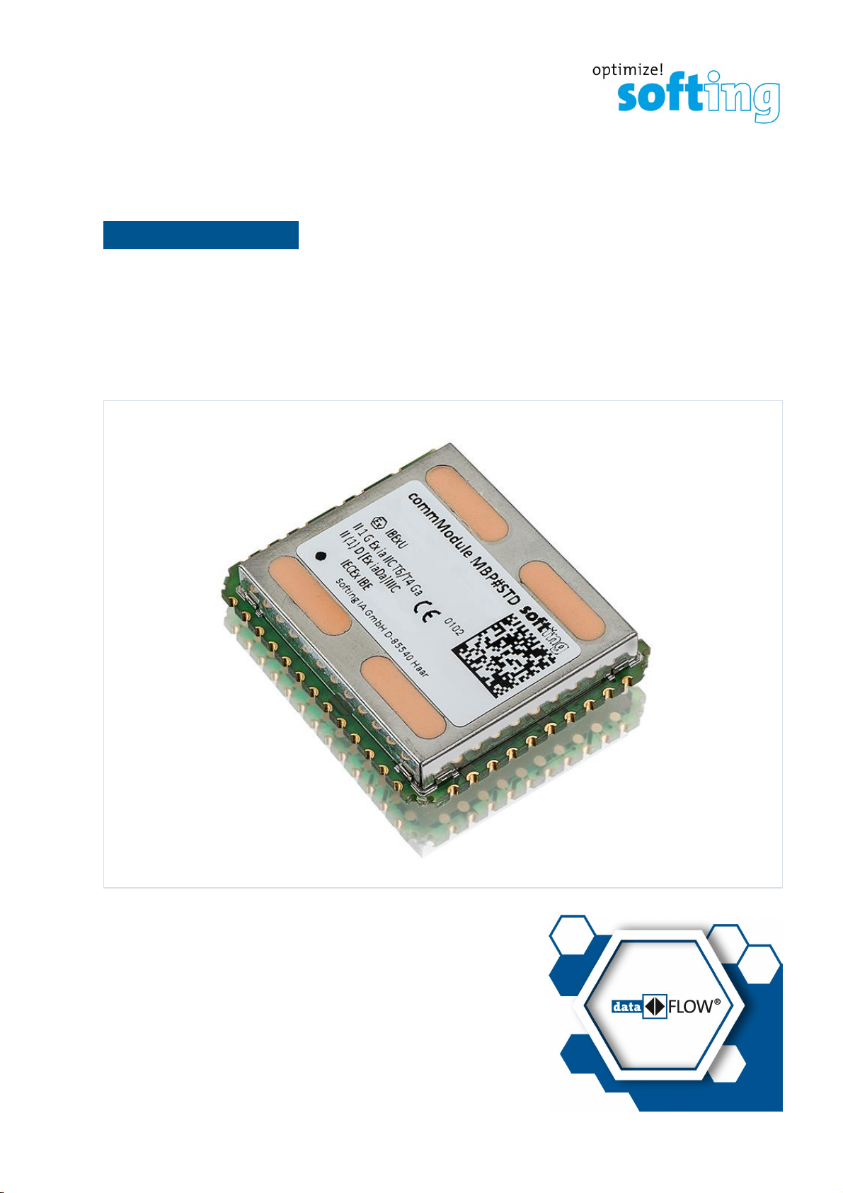
The commModule MBP is a surface mountable fieldbus communication module with minimum footprint.
It is typically integrated into an intelligent field device mapping industrial intrinsic safe fieldbus Profibus PA
and Foundation Fieldbus to the field device.
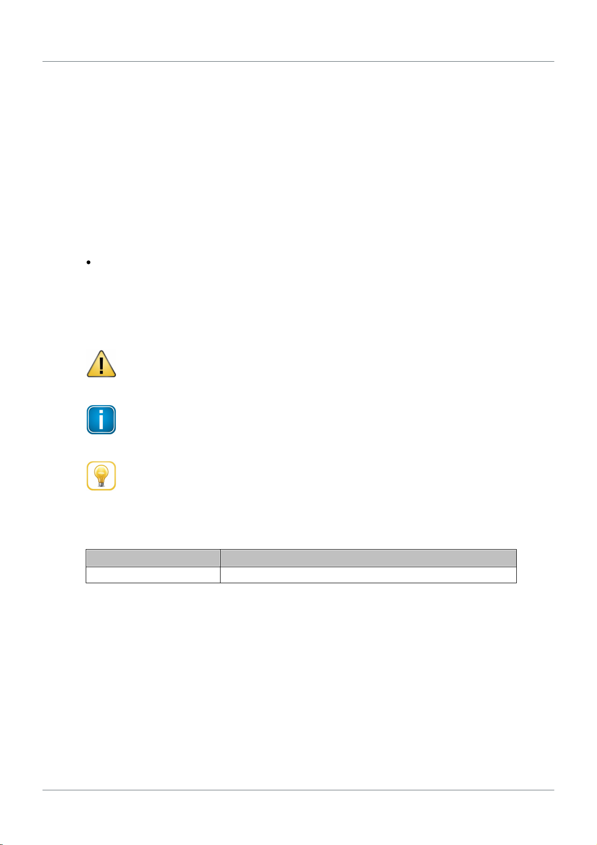
2.1 Diagram
The block diagram below shows the design of the commModule MBP:
12
2.2 Intended use
This product has been designed to be integrated as a system component by a qualified hardware engineer.
6
© Softing Industrial Automation GmbH
Chapter 3 - Interface
Signal Name
Pin No.
I/O*
Description
TXD9_PB7
1DOTX Interface signal for HART
#RTS9_PB5
2DOLow active RTS signal for HART
RXD9_PB6
3DIRX Interface signal for HART
GPIO_PA4
4
GPIO
For future use
GPIO_PE6
5
GPIO, AI
For future use
#CTS9_PB4
6DILow active CTS signal for HART
3V15
7
VCC
Do not use. Internal supply voltage
GND
8
Ground
Ground
GPIO_PE2
9
GPIO
For future use
GPIO_PE5
10
GPIO, AI
For future use
GPIO_PE7
11
GPIO, AI
For future use
GPIO_PE1
12
GPIO
For future use
PROT_SEL_P27 / TCK
13DIProtocol Select: FF/PA, Programming interface
TDO14DBG
Programming interface
GND
15
Ground
Ground
3
Interface
This section describes the signals available on the module via the PCB solder pads on the edge of the PCB.
3.1 Orientation
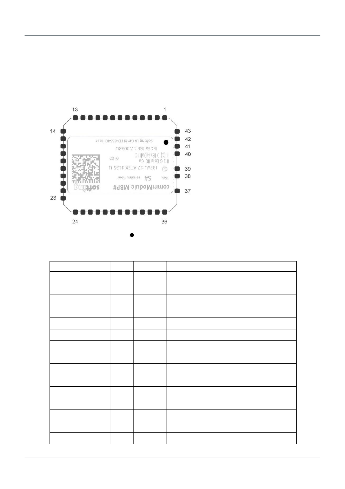
Top view on commModule
The position of Pin 1 is marked on the label.
3.2 Pin number and signal description
© Softing Industrial Automation GmbH
7

commModule MBP - Hardware Manual
RXD7_P92
16DIRX Interface signal for Debug Console (PD 33k)
TXD7_P90
17DOTX Interface signal for Debug Console
DA118AO
For future use
GND
19
Ground
Ground
3V_OUT
20POPower Output 3.15V
6V2_OUT
21POPower Output 6.2V
SIM_EN_P31
22
DBG
Simulate Enable
GPIO_P23
23
GPIO
For future use
GPIO_P22
24
GPIO
For future use
GPIO_P21
25
GPIO
For future use
GPIO_P20
26
GPIO
For future use
GPIO_PC6
27
GPIO
For future use
GPIO_PC7
28
DBG/GPIO
For future use
GPIO_PC5
29
GPIO
For future use
GPIO_PC4
30
GPIO
For future use
EMLE
31
DBG
Programming Interface
TDI32DBG
Programming interface
GPIO_PD2
33
GPIO
For future use
#RESET
34
DBG
Programming interface
FINED
35
DBG
Programming interface (do not pullup)
GND
36
Ground
Ground
FB_P_NF
37FBDo not use
FIELDBUS_N
38FBFieldbus
FIELDBUS_P
39FBFieldbus
FDE_PO
40FBFDE, connect to Pin 41
FDE_PI
41FBFDE, connect to Pin 40
FDE_NO
42FBFDE, connect to Pin 43
FDE_NI
43FBFDE, connect to Pin 42
* AI = Analog Input, AO = Analog Output, DI = CMOS Digital Input, DO = CMOS Digital Output, GPIO = General
Purpose CMOS Digital Input/Output, PO = Power Output, DBG = Programmer Interface, FB = Fieldbus, PD
Pulldown, PU Pullup
8
© Softing Industrial Automation GmbH
3.3 Pullups and pulldowns
Signal Name
Description
14-pin Renesas Fine
Interface
TDO
Not required for debugging.
Only used for internal flash programming with
Renesas Flash Programmer
5
TDI
Not required for debugging.
Only used for internal flash programming with
Renesas Flash Programmer
11
FINEC
Programming Interface
1
FINED
Programming Interface
7
PC7
Programming Interface
10
#RESET
Programming Interface
13
GND
Ground
2, 12, 14
3V15
Internal supply voltage
8
EMLE
Programming Interface
4
CAUTION
The memory blocks are reserved for the firmware. They must not be modified as this will
invalidate the software license and damage the commModule MBP. Only programming project
files provided by Softing shall be used to reprogram the module.
Weak pullups are provided on all GPIO pins. Pullups for TDO and TDI are not included on the CommModule
MBP and must be included on the application base board (pullup to Pin 7 of CommModule MBP).
RXD7_P92: internal pulldown 33k
3.4 Flash programming and debugging interface
The following signals of the microcontroller are required for flash programming.
See the commModule MBP Evaluation Kit manual for details. The usage of this interface is detailed in
document "E1/E20 Emulator – additional document for User’s Manual (RX User System Design) from
Renesas".
Chapter 3 - Interface
3.5 Fault Disconnect Equipment
External fault disconnect equipment (FDE) can be optionally added using the assigned FDE pins.
If not in use, connect signal FDE_PO to FDE_PI and signal FDE_NO to FDE_NI.
3.6 Simulate enable
Fieldbus conformance testing requires switching the application to simulation mode.
Simulation mode is enabled by signaling low on pin SIM_EN_P31.
For the registration of the final device by the FieldComm Group this signal must be accessible to the
fieldbus testing personnel.
© Softing Industrial Automation GmbH
9

commModule MBP - Hardware Manual
Fieldbus Protocol
PROT_SEL_P27
description
Fieldbus Foundation FF
High
(internal pullup)
Leave open
The commModule MBP is operating in
Foundation Fieldbus (FF) mode.
Profibus PA
Low
connect to GND
The commModule MBP is operating in Profibus
PA mode.
Parameter
Symbol
Min
Max
Unit
Test Conditions
DI: input low voltage
V
IL
Vcc x 0.2
V
DI: input high voltage
VIHVcc x 0.8
V
DO: output low voltage
V
OL
0.5
V
IOL = 1mA
DO: output high voltage
VOHVcc – 0.5
V
IOH = -1mA
4
Electrical specifications
4.1 Protocol select
This pin is scanned during start-up.
4.2 Operating conditions
Unless otherwise noted, all specifications apply over the specified operating temperature range.
4.3 Port input and output
The communication module has the following port input and port output specification at Vcc = 3.2V± 4%.
Analog Input
The commModule MBP incorporates a 12bit-A/D converter with a reference voltage of 3.0V
Power Output:
The power budget to supply a connected system from fieldbus is limited.
It is dependent on the rated current from fieldbus, which is adjustable in software
from IN = 10mA to 26mA.
Available output power:
P
= approx. 90mW on 6V2_OUT, with I
omax
or:
P
= approx. 70mW on 3V_OUT, with I
omax
When both power outputs are used, the available power budget is between 70 and 90mW. The slew rate
is controlled. The rise time is 1.43ms. The output current is not limited on the commModule MBP.
10
PO_6V2
PO_3V_OUT
= I
– 10mA
N
= (IN – 10mA) / 0.7
© Softing Industrial Automation GmbH

Chapter 4 - Electrical specifications
Note
If the available power budget is exceeded the commModule MBP may reset.
Parameter
Nom
Min
Max
Unit
3V_OUT
Io = 1mA
3.2
3.1
3.3
V
6V2_OUT (internal series resistance 10 Ohms)
Io = 1mA
6.2
6.05
6.3
V
Fieldbus:
Physical Layer according to IEC 61158-2 type 3 voltage mode, 31.25kBit/s.
Rated current adjusted in software to In = 10mA up to 26mA.
Powered from Fieldbus 9V to 32V (non hazardous location).
Use in hazardous locations:
Limitation on fieldbus power supply applies for different use cases. See also Operating conditions for use
in hazardous environment .
12
© Softing Industrial Automation GmbH
11

commModule MBP - Hardware Manual
Parameter
Units
Min
Max
Note
operating temperature
°C
-40
80
storage temperature
°C
-40
85
humidity
°rH1090
non condensing
Use Case
Input Supply
Temperature
Class
Ambient
Temperature Range
commModule
Internal fused with
62mA
FISCO
or:
EX ia IIB, Ui =17.5V, Ii =380mA
or:
EX ia IIC, Ui = 24V, Ii = 250mA
T4
-40°C to +80°C
5
Environmental specifications
5.1 Temperature
Absolute Maximum Ratings:
Storage temperature: -40°C to + 85°C.
Stresses exceeding maximum ratings may damage the device. Maximum ratings are stress ratings only.
Functional operation above the recommended operating conditions is not implied. Extended exposure to
stresses above the recommended operating conditions may affect device reliability.
Normal Operating Conditions (module soldered):
Fieldbus current adjustable from 10mA to 26mA.
Operating conditions for use in hazardous environment:
Operating temperature is dependent on intrinsic safe input parameters.
Operating Conditions for use in hazardous environment with external fuse.
Additional requirements apply for the design of the host PCB.
For further information see the ATEX EC type examination certificate .
5.2 MTBF calculation
MTBF calculated according to SN29500:
@40°C: 3.655.879 hours
@70°C: 1.142.849 hours
Conditions: Standard SN29500, continuous operation
12
22
© Softing Industrial Automation GmbH

5.3 Certifications
ROHS
The commModule MBP is ROHS compliant.
ATEX / IECEx:
IECEx IBE 17.0038U
Ex ia IIC Ga
[Ex ia Da] IIIC
IBExU17ATEX1135 U
II 1G Ex ia IIC Ga
II (1) D [Ex ia Da] IIC
Chapter 5 - Environmental specifications
© Softing Industrial Automation GmbH
13

commModule MBP - Hardware Manual
6
Mechanical specification
The weight of a potted variant (commModule MBP#STD) is approximately 15 gram. The weight of the non-
potted variant (commModule MBP#STD_NOP) is 8 gram.
6.1 Module dimensions
The dimensions below are shown in millimeters.
14
Bottom view
© Softing Industrial Automation GmbH

6.2 Host PCB layout
Note
The host PCB footprint must not contain any exposed copper under the module except the
pads interfacing the CommModule MBP to avoid any contact with traces on the module.
Recommended footprint
Chapter 6 - Mechanical specification
The PCB footprint dimensions may be modified based on user experience and/or process capability.
Routing under the CommModule MBP
© Softing Industrial Automation GmbH
15

commModule MBP - Hardware Manual
Note
It is recommended to include 4 vias on the host PCB near the corners (not in keep out area) to
avoid tilting of the CommModule MBP during soldering.
Note
The recommended stencil thickness is 0.12 to 0.15mm.
Note
The schematic library and PCB library for the Altium Designer can be download here:
Intrinsic safety:
1. Ensure there is no copper within 0.5mm of the marked Keep Out Area on the host PCB.
2. Ensure a clearance of 2mm between signals on Pin 40 – 43 to all other pins.
3. Ensure a clearance of 2mm between fieldbus on Pin 37 – 39 to all other pins and Pin 37 to Pin 39.
Solderpaste
16
© Softing Industrial Automation GmbH

6.3 Mounting process
Note
It is recommended to perform electrical, climate, stress and vibration tests on the final
assembled product to verify that the manufacturing process has not damaged the
commModule MBP. CommModule MBP are moisture sensitive devices.
Note
Variant commModule MBP #STD must be soldered by hand.
The commModule MBP contains highly sensitive electronic circuitry and is an Electrostatic
Sensitive Device (ESD). Observe precautions for safe handling! Failure to observe these
precautions can result in severe damage to the module.
The PCB is made of FR4 and has a NiAu surface finish. We strongly recommend that commModule MBP
modules are not soldered more than once after shipping by Softing.
The soldering of the communication module is compliant with RoHS directive 2011/65.
Reflow recommendations
The following temperatures and times are recommended for variant commModule MBP #STD_NOP:
Ramp up rate 3°C/second max
Maximum time maintained above 217°C 40 -60 seconds
Peak reflow temperature 245°C
Ramp down rate 4°C/second max
Chapter 6 - Mechanical specification
6.4 ESD handling precautions
6.5 Packaging and labeling
CommModule MBP are moisture sensitive devices. They are shipped in ESD safe trays measuring
approximately 136 x 315 mm.
Storage and Drying
The packaging may not exceed the max. temperature of 60°C.
Labeling
© Softing Industrial Automation GmbH
17

commModule MBP - Hardware Manual
7
Special conditions for safe use
Please read and follow the instructions in this manual.
If the notes stated in this excerpt are not observed or in case of inappropriate handling of the device,
our liability is waived.
The details of this user manual have to be observed as have to be the conditions for use and the
applicable details stated on the marking, type labeling and accompanying documentation of each device.
The device is only approved for intended and appropriate use. In case of non-compliance, the warranty
and manufacturer’s liability do no longer apply!
It has to be ensured that only such equipment is installed which complies with the types of protection
applicable to the relevant zones!
All connected electrical equipment has to be suitable for the respective intended use.
Equipment Protection Level Ga requires an enclosure according to IEC 60079-0. Mechanical strength tests
on enclosures, e.g. degree of protection (IP), thermal endurance tests, impact test, fall test are not
applicable for the commModule MBP as a bare module.
7.1 Galvanic isolation
The circuits of the commModule MBP have no galvanic isolation. All signals are galvanically connected
together.
7.2 Safety block diagram
The following block diagram shows the commModule MBP:
18
© Softing Industrial Automation GmbH

7.3 Installation
Pin
Signal
Creepage and clearance
Pin 1 to 36
GPIO, GND, DBG
No requirement on creepage distances between these
signals.
Clearance and creepage distance to all other signals
with level of protection 10V according to table 5 in
IEC 60079-0
Pin 37
FB_P_NF
Clearance and creepage distance to all other signals
except FIELDBUS_N
with level of protection 30V according to table 5 in
IEC 60079-0
Pin 38, 39
FIELDBUS_P, FIELDBUS_N
No requirement on creepage distances between these
signals.
Clearance and creepage distance to all other signals
The commModule MBP must be installed by qualified personnel only.
Ensure that the equipment installed complies with the types of protection relevant to the applicable zones
and categories and with local requirements for electrical equipment used in explosive areas associated
with explosive atmosphere.
The following points must be considered when deploying the unit:
The device must be used as intended by the manufacturer
Do not use this device when damaged.
Do not use this device when certification information is illegible.
Observe storage conditions.
Clean installation space.
Installation done according to instructions.
Do not put stress on the system by bending or torsion.
Connecting improper or non Ex certified equipment invalidates Ex approval of device.
Chapter 7 - Special conditions for safe use
Electrical parameters of connected devices must match the values described in the technical section.
Local requirements for electrical equipment for use with hazardous location associated with explosive
atmosphere shall be considered for installation.
This device has no housing and must be protected in a cabinet against splash water, dirt, moisture
mechanical force exceeding pollution degree 1.
7.4 Isolation and creepage distances
Following creepage and clearance distances and separations must be observed when integrating
commModule MBP.
© Softing Industrial Automation GmbH
19

commModule MBP - Hardware Manual
with level of protection 30V according to table 5 in
IEC 60079-0
Pin 40 to 43
FDE_PO, FDE_PI,
FDE_NO, FDE_NI
No requirement on creepage distances between these
signals.
Clearance and creepage distance to all other signals
with level of protection 30V according to table 5 in
IEC 60079-0
7.5 Label
The commModule MBP is marked with a label similar to the example below.
7.6 Maintenance and spare parts
The device does not require any maintenance.
In case of malfunctioning or failure, disassemble the device or the affected part and return this device to
Softing for repair.
20
© Softing Industrial Automation GmbH

Chapter 8 - CE Compliance
8
CE Compliance
This device complies with the following EC directives:
EC directive 2014/30/EU "EMC directive”
EC directive 2014/34/EU "ATEX"
EC directive 2011/65/EU "RoHS"
© Softing Industrial Automation GmbH
21

commModule MBP - Hardware Manual
8.1 ATEX EC type examination certificate
22
© Softing Industrial Automation GmbH

Chapter 8 - CE Compliance
© Softing Industrial Automation GmbH
23

commModule MBP - Hardware Manual
24
© Softing Industrial Automation GmbH

Chapter 8 - CE Compliance
© Softing Industrial Automation GmbH
25

commModule MBP - Hardware Manual
26
© Softing Industrial Automation GmbH

8.2 IECEx Certificate of Conformity
Chapter 8 - CE Compliance
© Softing Industrial Automation GmbH
27

commModule MBP - Hardware Manual
28
© Softing Industrial Automation GmbH

Chapter 8 - CE Compliance
© Softing Industrial Automation GmbH
29

commModule MBP - Hardware Manual
30
© Softing Industrial Automation GmbH

Chapter 8 - CE Compliance
© Softing Industrial Automation GmbH
31

commModule MBP - Hardware Manual
32
© Softing Industrial Automation GmbH

Chapter 8 - CE Compliance
© Softing Industrial Automation GmbH
33

commModule MBP - Hardware Manual
34
© Softing Industrial Automation GmbH

8.3 Declaration of Conformity
Chapter 8 - CE Compliance
© Softing Industrial Automation GmbH
35

Softing Industrial Automation GmbH
Richard-Reitzner-Allee 6
85540 Haar / Germany
http://industrial.softing.com
Tel: + 49 89 45 656-340
Fax: + 49 89 45 656-488
info.idn@softing.com
 Loading...