

USB97CFDC
USB Floppy Disk Controller
FEATURES
3.3 Volt, Low Power Operation
Complete USB Specification 1.1 Compatibility
- Includes USB Transceiver
- Based on an Enhanced Version of SMSC’s
Industry Proven USB97C100 USB Controller
Complete System Solution Including USB Mass
Storage Class Compliant Win98/2000 Driver and
Firmware
- Supports 640K, 720K, 1.44M, 1.2M Windows 98
J, and 1.2M NEC DOS 6.x Formats
- Supports Both the UFI and SFF8070i Command
Sets
- Supports USB Mass Storage Compliant
Bootable Floppy BIOS
- 4ms Seek Times
- USB 1.1 Compliance, Including Low Power
Device Class SUSPEND Mode Operation and
Power Control of Disk Drive
- Disk Drive Feedback of Readiness Upon Power
Re-Application Option
- Option for Ultra High Performance Using
Additional Caching SRAM
- Support for Floppy Drive Power Control
Contains SMSC’s Industry Proven Floppy Disk
Controller
- Licensed CMOS 765B Floppy Disk Controller
- Supports Single Normal or Three Mode Floppy
Drives
- Supports Vertical Recording Format and High
Capacity Drives in User Written Firmware
Applications
- Detects All Overrun and Underrun Conditions
- Sophisticated Power Control Circuitry (PCC)
Including Multiple Powerdown Modes for
Reduced Power Consumption
Enhanced Digital Data Separator
- 1 Mbps, 500 Kbps, 300 Kbps, 250 Kbps Data
Rates
- Programmable Precompensation Modes
Intelligent Auto Power Management
- <300µA SUSPEND Current
- <75mA Operating Current
External Program Memory Interface
- 32K Byte Code Space (Supplied Firmware
Requires 16KB Memory)
- Flash, SRAM, or EPROM Memory
4KB Internal Buffer SRAM for High Performance
Operation
Optional External Cache Memory
- Up to 16K x 8 External SRAM may be Used for
Custom Tape/ Drive Applications
Integrated 14.318 MHz Crystal Driver Circuit
100 pin TQFP package (12.0 x 12.0 mm footprint)
- 25% smaller body size than other 100 pin TQFP
packages
ORDERING INFORMATION
Order Number: USB97CFDC-MN
100 Pin TQFP Package
SMSC DS – USB97CFDC Rev. 12/15/2000

© STANDARD MICROSYSTEMS CORPORATION (SMSC) 2000
80 Arkay Drive
Hauppauge, NY 11788
(631) 435-6000
FAX (631) 273-3123
Standard Microsystems is a registered trademark of Standard Microsystems Corporation, and SMSC is a trademark of Standard Microsystems
Corporation. Product names and company names are the trademarks of their respective holders. Circuit diagrams utilizing S MSC products are incl uded
as a means of illustrating typical applications; consequently complete information sufficient for construction purposes is not necessarily given. Although
the information has been checked and is believed to be accurate, no responsibility is assumed for inaccuracies. SMSC reserves the right to make
changes to specifications and product descriptions at any time without notice. Contact your local SMSC sales office to obtain the latest speci fications
before placing your product order. The provision of this information does not convey to the purchaser of the semiconductor devices described any
licenses under the patent rights of SMSC or others. All sales are expressly conditional on your agreement to the terms and conditions of the most
recently dated version of SMSC's standard Terms of Sale Agreement dated before the date of your order (the "Terms of Sale Agreem ent" ). T he product
may contain design defects or errors known as anomalies which may cause the product's functions to deviate from published specifications. Anom aly
sheets are available upon request. SMSC products are not designed, intended, authorized or warranted for use in any life support or other application
where product failure could cause or contribute to personal injury or severe property damage. Any and all such uses without prior written approval of an
Officer of SMSC and further testing and/or modification will be fully at the risk of the customer. Copies of this document or other SMSC literature, as well
as the Terms of Sale Agreement, may be obtained by visiting SMSC’s website at http://www.smsc.com.
SMSC DISCLAIMS AND EXCLUDES ANY AND ALL WARRANTIES, INCLUDING WITHOUT LIMITATION ANY AND ALL IMPLIED WARRANTIES
OF MERCHANTABILITY, FITNESS FOR A PARTICULAR PURPOSE, TITLE, AND AGAINST INFRINGEMENT, AND ANY AND ALL WARRANTIES
ARISING FROM ANY COURSE OF DEALING OR USAGE OF TRADE.
IN NO EVENT SHALL SMSC BE LIABLE FOR ANY DIRECT, INCIDENTAL, INDIRECT, SPECIAL, PUNITIVE, OR CONSEQUENTIAL DAMAGES,
OR FOR LOST DATA, PROFITS, SAVINGS OR REVENUES OF ANY KIND; REGARDLESS OF THE FORM OF ACTION, WHETHER BASED ON
CONTRACT, TORT, NEGLIGENCE OF SMSC OR OTHERS, STRICT LIABILITY, BREACH OF WARRANTY, OR OTHERWISE; WHETHER OR NOT
ANY REMEDY IS HELD TO HAVE FAILED OF ITS ESSENTIAL PURPOSE; AND WHETHER OR NOT SMSC HAS BEEN ADVISED OF THE
POSSIBILITY OF SUCH DAMAGES.
SMSC DS – USB97CFDC Page 2 Rev. 12/15/2000

GENERAL DESCRIPTION
The USB97CFDC is an integration of the USB97C102 Enhanced Multi-Endpoint USB Peripheral Controller, without
its integrated hub functions, and the SMSC Floppy Disk Controller used in many of its Super IO products, such as
the FDC37C869. Special care in the interconnection of the two devices has been taken to assure the lowest possible
system current draw (<300µA) during SUSPEND mode operation.
Provisions for external Flash Memory up to 32K bytes for program storage is provided.
Although not required for standard floppy operation, provisions for 16K bytes of external buffer SRAM, in addition to
that included in the USB97C102 core, is also provided for extended applications, such as tape drives and for other
special applications.
Several pins are provided for controlling external power control elements and sensing specialized drive functions.
Note: SMSC has developed and supplies firmware and drivers for this device to implement a standard three mode
or dual mode Floppy Disk Drive system with drive power control. If the customer desires to develop his own
firmware and/or drivers for this system, he may contact SMSC to obtain a complete engineering
specification which details all the internal block functions and register maps of the USB97CFDC to allow
custom programs to be written for this device.
SMSC DS – USB97CFDC Page 3 Rev. 12/15/2000

TABLE OF CONTENTS
GENERAL DESCRIPTION............................................................................................................................3
DESCRIPTION OF PIN FUNCTIONS...........................................................................................................5
PIN CONFIGURATION .................................................................................................................................6
BLOCK DIAGRAM........................................................................................................................................7
PIN DESCRIPTIONS.....................................................................................................................................7
BUFFER TYPE DESCRIPTIONS............................................................................................................10
BOARD TEST MODE OPERATION...........................................................................................................10
DC PARAMETERS .....................................................................................................................................11
AC PARAMETERS......................................................................................................................................12
USB PARAMETERS...................................................................................................................................15
USB DC PARAMETERS.........................................................................................................................15
USB AC PARAMETERS.........................................................................................................................16
MECHANICAL OUTLINE............................................................................................................................18
APPENDIX A:..............................................................................................................................................19
USB97CFDC TYPICAL APPLICATION..................................................................................................19
SMSC PROVIDED SOFTWARE FOR USB97CFDC .............................................................................20
USB97CFDC REVISIONS...........................................................................................................................20
SMSC DS – USB97CFDC Page 4 Rev. 12/15/2000

DESCRIPTION OF PIN FUNCTIONS
FLOPPY DISK INTERFACE (14 Pins)
nTRK0 nINDEX nWRTPRT nDSKCHG
nRDATA DRVDEN0 DRVDEN1 nSTEP
nWDATA nWGATE nHDSEL nDIR
nDSO nMTR0
USB+ USB- AVDD AGND
FD0 FD1 FD2 FD3
FD4 FD5 FD6 FD7
FA0 FA1 FA2 FA3
FA4 FA5 FA6 FA7
FA8 FA9 FA10 FA11
FA12 FA13 FA14 FA15
nFRD nFCE
SD0 SD1 SD2 SD3
SD4 SD5 SD6 SD7
SA0 SA1 SA2 SA3
SA4 SA5 SA6 SA7
SA8 SA9 SA10 SA11
SA12 SA13 nMEMR nMEMW
nMEMEN OPTEN nDRVRDY nFDPWR
XTAL1/CLKIN XTAL2 nRESET nTEST
TST_OUT nTESTEN
POWER, GROUNDS, and NO CONNECTS (22 Pins)
USB INTERFACE (4 Pins)
FLASH ROM INTERFACE (26 Pins)
SRAM/IO INTERFACE (24 Pins)
MISC (10 Pins)
SMSC DS – USB97CFDC Page 5 Rev. 12/15/2000
PIN CONFIGURATION
nRDATA
nWRTPRT
nTRK0
nINDEX
nHDSEL
nWGATE
nWDATA
nSTEP
nDIR
GND
nDS0
nMTR0
DRVDEN0
AGND
USB+
VDD
USB-
AVDD
FA11
FA9
FA8
FA13
FA14
GND
N.C.
nDSKCHG
DRVDEN1
N.C.
GND
N.C.
GND
VDD
N.C.
SD7
SD6
SD5
SD4
GND
SD3
SD2
SD1
SD0
VDD
N.C.
N.C.
N.C.
nMEMR
nMEMW
SA12
SA11
75
51
FA15
FA12
FA7
FA6
FA5
FA4
FA3
GND
FA2
FA1
FA0
VDD
USB97CFDC
1
25
FD0
FD1
FD2
FD3
FD4
FD5
FD6
FD7
nFCE
FA10
nFRD
GND
nFDPWR
SA9
SA8
SA7
SA6
SA5
SA4
SA3
SA2
SA1
SA0
SA10
SMSC DS – USB97CFDC Page 6 Rev. 12/15/2000
GND
VDD
SA13
nTEST
nTESTEN
XTAL1/CLKIN
GND
XTAL2
N.C.
nRESET
OPTEN
TSTOUT
nMEMEN
nDRVRDY
BLOCK DIAGRAM
To USB Bus
Option
Select/
Drive
Control
nTRK0, nINDEX,
nWRTPRT, nDSKCHG
nRDATA, DRVDEN0,
DRVDEN1, nWDATA,
nWGATE, nHDSEL,
nDIR, nMTR0, nDS0,
nSTEP
Flash/
SRAM
Interface
nMEMEN
nOPTEN
nDRVRDY
nFDPWR
DRIVE
INTERFACE
nFRD
nFCE
GPIO
FD[7:0]
FA[15:0]
CLOCK
CONTROL
IRQ0
FLOPPY DISK
CONTROLLER
High Speed
USB
XCVR
8051 CPU
Serial Interface Engine
SIE DMA
RX/
TX
Queue
DRQ2
TC
nDAK2
nIOW
nIOR
nCE
ADDRESS
DECODE
AEN
End Point
Control
Arbiter
8237
Memory
Management
4k Data Buffer RAM
SA[13:0]
nMEMW
nMEMR
SD[7:0]
Unit
SRAM
Interface
Map RAM
Pin Descriptions
PIN NO. NAME SYMBOL
75 Read Disk
Data
69 Write
Data
71 Head
Select
67 Direction
Control
68 Step Pulse nSTEP OD12 This active low high current driver issues a low
76 Disk Change nDSKCHG IS This input senses that the drive door is open or
BUFFER
TYPE
DESCRIPTION
FLOPPY DISK INTERFACE
nRDATA IS Raw serial bit stream from the disk drive, low
active. Each falling edge represents a flux
transition of the encoded data.
nWDATA OD12 This active low high current driver provides the
encoded data to the disk drive. Each falling edge
causes a flux transition on the media.
nHDSEL OD12 This high current output selects the floppy disk
side for reading or writing. A logic "1" on this pin
means side 0 will be accessed, while a logic "0"
means side 1 will be accessed.
nDIR OD12 This high current low active output determines the
direction of the head movement. A logic "1" on
this pin means outward motion, while a logic "0"
means inward motion.
pulse for each track-to-track movement of the
head.
that the diskette has possibly been changed since
the last drive selection.
SMSC DS – USB97CFDC Page 7 Rev. 12/15/2000

BUFFER
PIN NO. NAME SYMBOL
TYPE
DESCRIPTION
63 DRVDEN 0 DRVDEN 0 OD12 An active low on this pin indicates a disk drive
spindle speed change from 300 RPM to 360 RPM
or 1.2M format disks in three mode drives. This
pin should be tied to the disk drives spindle speed
control input pin.
77 DRVDEN 1 DRVDEN1 OD12 Reserved for future use.
70 Write Gate nWGATE OD12 This active low high current driver allows current to
flow through the write head. It becomes active just
prior to writing to the diskette.
73 Track 0 nTRK0 IS This active low Schmitt Trigger input senses from
the disk drive that the head is positioned over the
outermost track.
72 Index nINDEX IS This active low Schmitt Trigger input senses from
the disk drive that the head is positioned over the
beginning of a track, as marked by an index hole.
74 Write Protect nWRTPRT IS This active low Schmitt Trigger input senses from
the disk drive that a disk is write protected. Any
write command is ignored.
64 Motor On 0 nMTR0 OD12 This active low open drain output selects motor
drive 0.
65 Drive Select 0 nDS0 OD12 This active low open drain output selects drive 0.
USB INTERFACE
59
61
USB Bus
Data
USBUSB+
IO-U These pins connect to the USB data signals
through 33 ohm series resistors. The USB+ line
should be pulled up with a 5%, 1.5K ohm resistor
to indicate that this is a high speed USB device.
58 USB
Transceiver
AVDD This is the 3.3V supply to the internal USB
transceiver.
Supply
62 USB
Transceiver
AGND This is the supply ground for the internal USB
transceiver.
Ground
FLASH INTERFACE
31-38 Flash Memory
Data Bus
FD[7:0] IO8 These signals are used to transfer data between
the internal 8051 and the external FLASH program
memory.
50, 53, 54,
49, 57, 29,
Flash Memory
Address Bus
FA[15:0] O8 These signals address memory locations within
the FLASH memory.
56, 55, 48-
44, 42-40,
28 Flash Memory
nFRD O8 Flash ROM Read; active low
Read Strobe
30 Flash Memory
nFCE O8 Flash ROM Chip Select; active low
Chip Select
SRAM/IO INTERFACE
1-7,
9-13,
SRAM
Memory Bus
SA[13:0] O8 These signals provide the memory address to an
external SRAM buffer.
99,100
84-87,
89-92
SRAM
Memory Data
SD[7:0] I/O8 These signals are used to transfer data to/from the
SRAM Memory.
Bus
97 SRAM
Memory Read
Strobe
nMEMR O8 Memory read; active low
This active low signal indicates that data is to be
driven onto the data bus by the SRAM. Data will
be latched internal to the chip on the rising edge of
this signal
98 SRAM
Memory Wri te
Strobe
nMEMW O8 Memory write; active low
This active low signal indicates to the SRAM to
load data from the data bus on its rising edge.
SMSC DS – USB97CFDC Page 8 Rev. 12/15/2000

BUFFER
PIN NO. NAME SYMBOL
TYPE
DESCRIPTION
MISCELLANEOUS
17 Crystal
Input/External
Clock Input
XTAL1/
CLKIN
ICLKx 14.318Mhz Crystal or clock input.
This pin can be connected to one terminal of the
crystal or can be connected to an external
14.318Mhz clock when a crystal is not used.
18 Crystal
Output
XTAL2 OCLKx 14.318Mhz Crystal
This is the other terminal of the crystal, or left
open when an external clock source is used to
drive XTAL1/CLKIN. It may not be used to drive
any external circuitry other than the crystal circuit.
23 SRAM Enable nMEMEN O24 An active low signal is output on this pin to enable
the optional external SRAM for extended FDC
write and read caching for ultra high performance
applications.
24 Option Enable OPTEN I Current firmware utilizes this input pin for
detecting the media density switch of the drive.
Various firmware options are available for different
polarities of this signal. Contact factory for
available firmware options. If this pin is not driven
by the drive, it should be tied low.
25 Drive Ready nDRVRDY I An active low signal on this pin from the floppy
disk drive, after DS0 goes active, indicates that
the system may activate MTR0. If the drive does
not supply this signal, this pin should be tied low.
26 Drive Power nFDPWR OD24 This active low signal is intended to activate an
external power switch, either in the drive or on the
system board, to supply power to the floppy disk
drive. It is active whenever the USB97CFDC is not
in SUSPEND mode.
21 RESET input nRESET IS This active low signal is used by the system to
reset the chip. The active low pulse should be at
least 100ns wide.
22 Test output TSTOUT O8 This signal is used for testing the chip via an
internal XNOR chain. User should normally leave
it unconnected.
15 Test input nTEST I This signal is a manufacturing test pin. It should
be tied to VDD for normal operation.
16 Test Enable nTESTEN I This active low signal places the device into board
test mode using the XNOR chain. For normal
operation this pin should be tied high. See Board
Test Mode Operation on page 10
POWER, GROUND, AND NO CONNECTS
14, 39, 60,
VDD +3.3V power
82, 93
8, 19, 27, 43,
GND Ground Reference
52, 66, 79,
81, 88
20, 51, 78,
80, 83, 94-96
NC No Connect. These pins should not be connected
externally.
SMSC DS – USB97CFDC Page 9 Rev. 12/15/2000

BUFFER TYPE DESCRIPTIONS
Table 1 - USB97CFDC Buffer Type Descriptions
BUFFER DESCRIPTION
I Input
IS Input with Schmitt trigger
O8 Output with 8mA drive
I/O8 Input/output with 8mA drive
OD12 Open drain….12mA sink
O24 Output with 24mA drive
OD24 Open drain….24mA sink
ICLKx XTAL clock input
OCLKx XTAL clock output
I/O-U See Table 6.
BOARD TEST MODE OPERATION
By driving the nTESTEN pin low, the device will be placed into a special test mode to allow verification of attachment
of the device to the circuit board. Every pin except the TSTOUT, XTAL2, and the power and ground pins become an
input to an XNOR chain, as shown below, to allow continuity to be tested on the board. This test should individually
toggle the state of the trace connected to the pin being examined for continuity, and the TSTOUT pin monitored for
toggle of state. If no toggle occurs, either the pin under test is discontinuous, or the TSTOUT pin is not connected on
the board
Pin1 Pin2 Pin3 Pin100
TSTOUT
SMSC DS – USB97CFDC Page 10 Rev. 12/15/2000

DC PARAMETERS
MAXIMUM GUAR ANTEED RATING S
Operating Temperature Range...........................................................................................................................0
Storage Temperature Range...........................................................................................................................-55
Lead Temperature Range (soldering, 10 seconds).....................................................................................................+325
Positive Voltage on any pin, with respect to Ground (Note 1)...................................................................................V
Negative Voltage on any pin, with respect to Ground....................................................................................................-0.3V
Maximum V
.................................................................................................................................................................. +3.6V
cc
Note 1: Maximum voltage on all I ty pe Inputs and the IS inputs, OD 12 and O D24 outputs for floppy disk drive interface is
5.25V
*Stresses above the specified parameters could cause permanent damage to the device. This is a stress rating only
and functional operation of the device at any other condition above those indicated in the operation sections of this
specification is not implied.
Note 2: When powering this device from laboratory or system power supplies, it is important that the Absolute Maximum
Ratings not be exceeded or device failure can result. Some power supplies exhibit voltage spikes on their outputs when
the AC power is switched on or off. In addition, voltage transients on the AC power line may appear on the DC output.
When this possibility exists, it is suggested that a clamp circuit be used.
o
C to +70oC
o
to +150oC
+0.3V
cc
o
C
DC ELECTRICAL CHARACTERISTICS (T
= 0°C - 70°C, Vcc = +3.3 V ± 10%)
A
PARAMETER SYMBOL MIN TYP MAX UNITS COMMENTS
I Type Input Buffer
Low Input Level
High Input Level
V
ILI
V
IHI
2.0
0.8 V
TTL Levels
V
ICLK Input Buffer
Low Input Level
High Input Level
V
ILCK
V
IHCK
2.2
0.4 V
V
Input Leakage
(All I and IS buffers)
Low Input Leakage
High Input Leakage
I
IL
I
IH
-10
-10
+10
+10
uAuAVIN = 0
= V
V
IN
CC
O8 Type Buffer
Low Output Level
High Output Level
Output Leakage
V
OL
V
OH
I
OL
2.4
-10
0.4
+10
V
V
UA
= 8 mA
I
OL
= -4 mA
I
OH
= 0 to V
V
IN
I/O8 Type Buffer
Low Output Level
V
OL
0.4
V
IOL = 8mA
(Note 1)
CC
High Output Level
Output Leakage
V
OH
I
OL
2.4
-10
+10
V
IOH = -4mA
µA
VIN = 0 to Vcc (Note 1)
OD12 Type Buffer
Low Output Level
Output Leakage
SMSC DS – USB97CFDC Page 11 Rev. 12/15/2000
V
OL
I
OL
-10
0.4
+10
V
IOL = 12mA
µA
VIN = 0 to Vcc (Note 1)

PARAMETER SYMBOL MIN TYP MAX UNITS COMMENTS
O24 Type Buffer
Low Output Level
High Output Level
Output Leakage
V
OL
V
OH
I
OL
2.4
-10
0.4
+10
OD24 Type Buffer
Low Output Level
Output Leakage
V
OL
I
OL
-10
0.4
+10
IO-U
Note 2
Supply Current Active
I
CC
30
75
Supply Current
Standby
I
CSBU
120
300
Note 1: Output leakage is measured with the current pins in high impedance.
Note 2: See Appendix A for USB DC electrical characteristics.
CAPACITANCE T
= 25°C; fc = 1MHz; VCC = 3.3V
A
LIMITS
PARAMETER SYMBOL MIN TYP MAX UNIT TEST CONDITION
Clock Input Capacitance C
Input Capacitance C
Output Capacitance C
IN
IN
OUT
20 pF
10 pF
20 pF
V
IOL = 24mA
V
IOH = -12mA
µA
VIN = 0 to Vcc (Note 1)
V
IOL = 24mA
µA
VIN = 0 to Vcc (Note 1)
MAµAAll outputs open.
All pins except USB pins
(and pins under test tied
to AC ground)
AC PA RAMETERS
CLOCKI
NAME DESCRIPTION MIN TYP MAX UNITS
t1 Clock Cycle Time for 14.318MHz 69.84 ns
t2 Clock High Time/Low Time for 24MHz 41.9/
tr, tfClock Rise Time/Fall Time (not shown) 5 ns
t1
t2
t2
FIGURE 1 - INPUT CLOCK TIMING
Table 2 – Input Clock Timing Parameters
27.9
27.9/
41.9
ns
SMSC DS – USB97CFDC Page 12 Rev. 12/15/2000

FA[0:19
t1
t5
FD[7 :0
nFRD
nFWR
t3 t4
t2
FIGURE 2 – FLASH READ TIMING
Table 3 – Flash Read Timing
NAME PARAMETER MIN TYP MAX UNITS
t1 FA[14:0] Address setup time to nFRD asserted 40 ns
t2 nFRD pulse width 110 ns
t3 FD[7:0] Data setup time to nFRD de-asserted 30 ns
t4 FD[7:0] Data hold time from nFRD de-asserted 0 ns
t5 FA[14:0] Address hold time from nFRD de-asserted 35 ns
t1 t5
SA[13:0
t4
SD [7:0
nME MW
t3
t2
FIGURE 3 – SRAM MEMORY WRITE TIMING
Table 4 – SRAM Memory Write Timing
NAME PARAMETER MIN TYP MAX UNITS
t1 SA[19:0] valid before nMEMWR asserted 10 ns
t2 nMEMWR pulse width 100 ns
t3 SD[7:0] Data setup time to nMEMWR de-asserted 50 ns
t4 SD[7:0] Data hold time from nMEMWR de-asserted 10 ns
t5 nMEMWR de-asserted to SA[13:0] invalid 10 ns
SMSC DS – USB97CFDC Page 13 Rev. 12/15/2000
SA[13:0
t1 t5
t4
SD [7 :0]
nME MR
t3
t2
FIGURE 4 - SRAM MEMORY READ TIMING
Table 5 – SRAM Memory Read Timing
NAME PARAMETER MIN TYP MAX UNITS
t1 SA[19:0] valid before nMEMRD asserted 10 ns
t2 nMEMRD pulse width 100 ns
t3 SD[7:0] Data setup time to nMEMRD de-asserted 50 ns
t4 SD[7:0] Data hold time from nMEMRD de-asserted 20 ns
t5 nMEMRD de-asserted to SA [13:0] invalid 10 ns
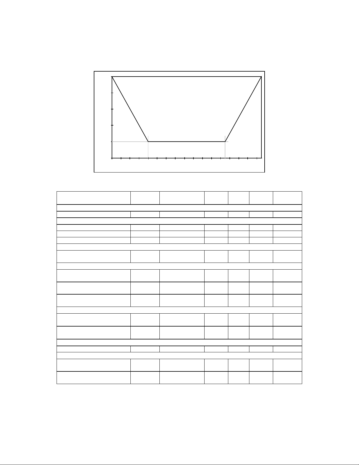
nDIR
nSTEP
t1
t2
t4
t3
nDS0
nINDEX
nRDATA
nWDATA
NAME
t1
t2
t3
t4
t5
t6
t7
t8
PARAMETER MIN
nDIR Set Up to nSTEP Low
nSTEP Active Time Low
nDIR Hold Time After nSTEP
nSTEP Cycle Ti m e
nDS0-1 Hold Time from nSTEP Low
nINDEX Pulse Width
nRDATA Active Time Low
nWDATA Write Data Width Low
t6
t7
t8
*X specifies one MCLK period and Y specifies one WCLK period.
MCLK = 16x Data Rate (at 500 Kbp/s MCLK = 8 MHz)
WCLK = 2x Data Rate (at 500 Kbp/s WCLK = 1 MHz)
t5
TYP
4
24
96
132
20
2
40
.5
MAX
UNITS
X*
X*
X*
X*
X*
X*
ns
Y*
FIGURE 5 - DISK DRIVE TIMING
SMSC DS – USB97CFDC Page 14 Rev. 12/15/2000
USB PARAMETERS
The following tables and diagrams were obtained from the USB specification
USB DC PARAMETERS
1.0
0.8
0.6
0.4
0.2
Minimum Differential Sensitivity (volts)
0.0
0.0 0.2 0.4 0.6 0.8 1.0 1.2 1.4 1.6 1.8 2.0 2.2 2.4 2.6 2.8 3.0 3.2
Common Mode Input Voltage (volts)
FIGURE 6 - DIFFERENTIAL INPUT SENSITIVITY OVER ENTIRE COMMON MODE RANGE
Table 6 - DC Electrical Characteristics
CONDITIONS
PARAMETER SYMBOL
Supply Voltage
Powered (Host or Hub) Port VBUS 4.4 5.25 V
Supply Current
Function ICC Note 4 100 mA
Un-configured Function (in) ICCINIT Note 5 100 uA
Suspend Device ICCS 100 uA
Leakage Current
Hi-Z State Data Line
ILO 0 V < VIN < 3.3
Leakage
Input Levels
Differential Input Sensitivity VDI |(D+) - (D-)|,
Differential Common Mode
VCM Includes VDI
Range
Single Ended Receiver
VSE 0.8 2.0 V
Threshold
Output Levels
Static Output Low VOL
Static Output High VOH
Capacitance
Transceiver Capacitance CIN Pin to GND 20 pF
Terminals
Bus Pull-up Resistor on
RPU
Root Port
Bus Pull-down Resistor on
RPD
Downstream Port
(NOTE 1, 2) MIN TYP MAX UNIT
-10 10 uA
V
0.2 V
and FIGURE 6
0.8 2.5 V
range
RL of 1.5 KΩ to
3.6 V
RL of 15 KΩ to
2.8 3.6 (3) V
GND
(1.5 KΩ +/- 5%)
(15 KΩ +/- 5%)
1.425 1.575
14.25 15.75
0.3 (3) V
kΩ
kΩ
Note 1: All voltages are measured from the local ground potential, unless otherwise specified.
Note 2: All timing use a capacitive load (CL) to ground of 50pF, unless otherwise specified.
Note 3: This is relative to VUSBIN.
Note 4: This is dependent on block configuration set by software.
Note 5: When the internal ring oscillator and waiting for first setup packet.
SMSC DS – USB97CFDC Page 15 Rev. 12/15/2000

USB AC PARAMETERS
C
L
C
L
Full Speed: 4 to 20ns at CL= 50pF
FIGURE 7 - DATA SIGNAL RISE AND FALL TIME
T
PERIOD
Differential
Data Lines
Rise Time
Differential
90%
Data Lines
10%
t
R
Crossover
Points
Consecutive
Transitions
N * T
PERIOD
+ T
xJR1
Paired
Transitions
N * T
PERIOD
+ T
xJR2
FIGURE 8 - DIFFERENTIAL DATA JITTER
90%
Fall Time
t
F
10%
T
PERIOD
Differential
Data L ines
T
Differential
Data Lines
Crossover
Crossover
Point Extended
Point
Diff. Data to
N * T
SE0 Skew
+ T
PERIOD
DEOP
Source EOP Width: T
Receiver EOP Width: T
FIGURE 9 - DIFFERENTIAL TO EOP TRANSITION SKEW AND EOP WIDTH
PERIOD
T
JR
T
JR1
Consecutive
Transitions
PERIOD
+ T
JR1
N * T
Paired
Transitions
PERIOD
+ T
JR2
N * T
FIGURE 10 - RECEIVER JITTER TOLERANCE
EOPT
EOPR1
T
JR2
, T
EOPR2
SMSC DS – USB97CFDC Page 16 Rev. 12/15/2000
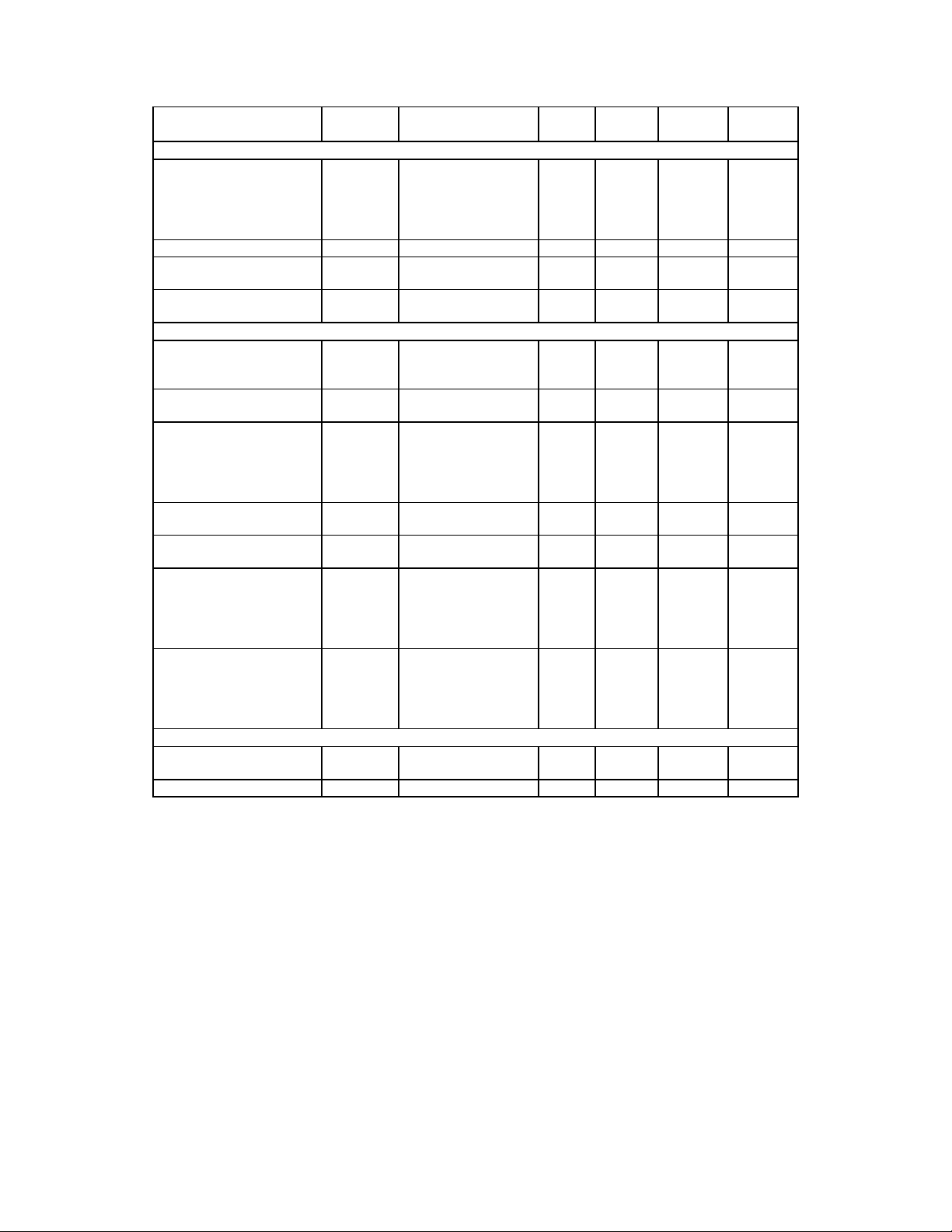
Table 2 - Full Speed (12Mbps) Source Electrical Characteristics
PARAMETER SYM
Driver Characteristics
Transition Time:
Rise Time
TR
CONDITIONS
(NOTE 1, 2, 3) MIN TYP MAX UNIT
Note 4,5 and
FIGURE 7
CL = 50 pF
4
20
ns
Fall Time
TF
CL = 50 pF
4
20
ns
Rise/Fall Time Matching TRFM (TR/TF) 90 110 %
Output Signal
VCRS 1.3 2.0 V
Crossover Voltage
Drive Output
ZDRV Steady State Drive 28 43
Ω
Resistance
Data Source Timing
Full Speed Data Rate TDRATE Ave. Bit Rate
11.95 12.03 Mbs
(12 Mb/s +/-
0.25%) Note 8
Frame Interval TFRAME 1.0 ms +/- 0.05% 0.999
1.0005 ms
5
Source Differential
Driver Jitter
To next Transition
TDJ1
TDJ2
Note 6, 7 and
FIGURE 8
-3.5
-4.0
3.5
4.0
ns
ns
For Paired Transitions
Source EOP Width TEOPT Note 7 and
160 175 ns
FIGURE 9
Differential to EOP
transition Skew
Receiver Data Jitter
Tolerance
To next Transition
For Paired Transitions
EOP Width at receiver
TDEOP Note 7 and
FIGURE 9
Note 7 and
FIGURE 10
TJR1
TJR2
Note 7 and
-2 5 ns
-18.5
-9
18.5
9.0
ns
ns
FIGURE 9
Must reject as EOP
Must Accept TEOPR1
TEOPR2
40
82
ns
ns
Cable Impedance and Timing
Cable Impedance (Full
ZO
(45 Ω +/- 15%)
38.75 51.75
Ω
Speed)
Cable Delay (One Way) TCBL 30 ns
Note 1: All voltages are measured from the local ground potential, unless otherwise specified.
Note 2: All timing use a capacitive load (CL) to ground of 50pF, unless otherwise specified.
Note 3: Full speed timings have a 1.5KΩ pull-up to 2.8 V on the D+ data line.
Note 4: Measured from 10% to 90% of the data signals.
Note 5: The rising and falling edges should be smoothly transiting (monotonic).
Note 6: Timing differences between the differential data signals.
Note 7: Measured at crossover point of differential data signals.
Note 8: These are relative to the 14.318 MHz crystal.
SMSC DS – USB97CFDC Page 17 Rev. 12/15/2000
MECHANICAL OUTLINE
FIGURE 11 - 100 PIN TQFP PACKAGE
MIN NOMINAL MAX REMARK
A ~ ~ 1.60 Overall Package Height
A1 0.05 ~ 0.15 Standoff
A2 1.35 1.40 1.45 Body Thickness
D 13.80 14.00 14.20 X Span
D/2 6.90 7.00 7.10
1
/2 X Span Measure from Centerline
D1 11.80 12.00 12.20 X body Size
E 13.80 14.00 14.20 Y Span
E/2 6.90 7.00 7.10
1
/2 Y Span Measure from Centerline
E1 11.80 12.00 12.20 Y body Size
H 0.09 ~ 0.20 Lead Frame Thickness
L 0.45 0.60 0.75 Lead Foot Length from Centerline
L1 ~ 1.00 ~ Lead Length
e 0.40 Basic Lead Pitch
0o3.5
o
o
7
Lead Foot Angle
W 0.13 0.16 0.23 Lead Width
R1 0.08 ~ ~ Lead Shoulder Radius
R2 0.08 ~ 0.20 Lead Foot Radius
ccc ~ ~ 0.08 Coplanarity
Note 1: Controlling Unit: millimeter
Note 2: Minimum space between protrusion and an adjacent lead is .007 mm.
Note 3: Package body dimensions D1 and E1 do not include the mold protrusion. Maximum mold protrusion is 0.25 mm
Note 5: Details of pin 1 identifier are optional but must be located within the zone indicated.
SMSC DS – USB97CFDC Page 18 Rev. 12/15/2000
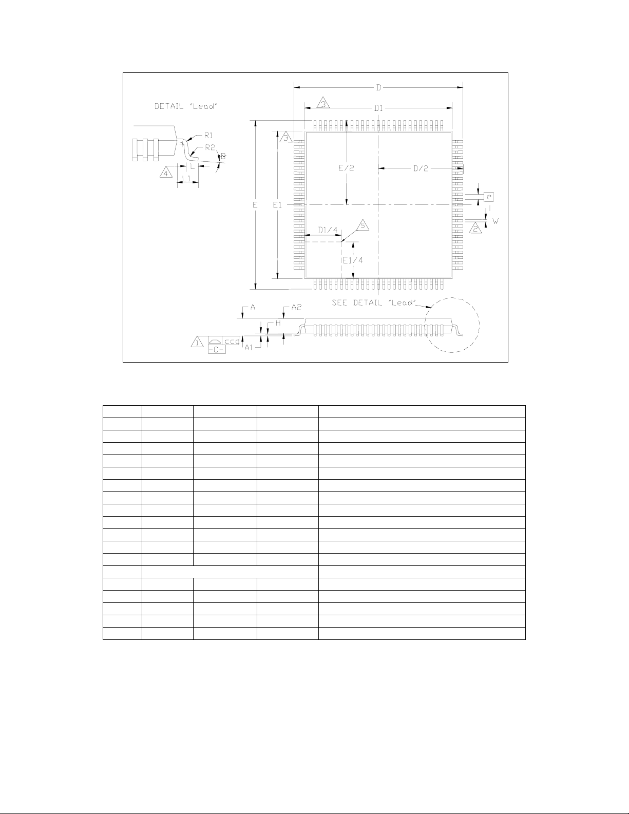
APPENDIX A:
USB97CFDC TYPICAL APPLICATION
Note: If SD
pins not used,
tie to ground to
prevent pins
from floating
during
suspend
mode.
VCC
VCC FVDD
C1
C2
.1uF
.1uF
RN2
10K x 8
VR1
3 2
VIN VOUT
+
C6
10uF
VDD
C10
C11
.1uF
.1uF
C3
.1uF
3.3V Regulator
GND
1
C12
.1uF
FVDD
3334
RN1
C4
.1uF
VDD
TP1
TP2
100
VDD
+
C5
10uF
nFDPWR
C13
C14
.1uF
.1uF
#DSKCHG
1K x 5
75747372717069686766656463626160595857565554535251
76
nDSKCHG
77
DRVDEN1
78
N.C.
79
GND
80
N.C.
81
GND
82
VDD
83
N.C.
84
SD7
85
SD6
86
SD5
87
SD4
88
GND
89
SD3
90
SD2
91
SD1
92
SD0
93
VDD
94
N.C.
95
N.C.
96
N.C.
97
nMEMR
98
nMEMW
99
SA12
SA11
SA10
12345678910111213141516171819202122232425
VCC
R7
Q1
MOSFET P
FVDD
1718
1920
2122
2324
2526
2728
2930
3132
#DIR
#WDATA
#WGATE
#TRK0
#WP
#RDATA
#HDSEL
#STEP
nSTEP
nTRK0
nINDEX
nHDSEL
nRDATA
nWGATE
nWDATA
nWRTPRT
USB97CFDC
SA9
SA8
SA7
SA6
SA5
SA4
GND
SA3
15K
R5
1µf
C8
1516
#MTR1
nDIR
SA2
1314
#DS0
GND
SA1
1112
#DS1
nDS0
SA0
#MTR0
nMTR0
SA13
#DSKSTAT
#INDEX
AGND
DRVDEN0
VDD
nTEST
12345678910
#1.2M
#HHDOUT
VDD
USB+
VDD
XTAL1/CLKIN
180K
R6
JP1
HDO
USB-
XTAL2
FVDD
FA9
FA8
FA11
AVDD
GND
N.C.
nRESET
TSTOUT
R4
1.5K
nDRVRDY
N.C.
GND
FA13
FA14
nFDPWR
nMEMEN
OPTEN
nDRVRDY
nDRVRDY
TP3
39pf
C7
Y1
14.318Mhz
15pf
C9
FLOPPY
U1
50
FA15
49
FA12
48
FA7
47
FA6
46
FA5
45
FA4
44
FA3
43
GND
42
FA2
41
FA1
40
FA0
39
VDD
38
FD0
37
FD1
36
FD2
35
FD3
34
FD4
33
FD5
32
FD6
31
FD7
30
nFCE
29
FA10
28
nFRD
27
GND
nFDPWR
26
Note: IF DRIVE
DOES NOT
SUPPLY
nDRVRDY OR
HDO SIGNAL,
THEY
SHOULD BE
TIED LOW AT
U1
HDO
VDD
U2
13
14
15
17
18
19
20
21
30
D0
D1
D2
D3
D4
D5
D6
D7
2
NC
3
NC
NC
28F256
R1 10ohm
R2
10ohm
A0
A1
A2
A3
A4
A5
A6
A7
A8
A9
A10
A11
A12
A13
A14
CE
OE
WE
VPP
Title
Size Document Number Rev
Date: Sheet
VCC
P1
1
VCC
2
D-
3
D+
4
R3
10K
5%
1/10W
12
11
10
9
8
7
6
5
27
26
23
25
4
28
29
22
24
31
1
GND
USB TYPE B
VDD
USB97CFDC Typical Application
B
11Wednesday, December 13, 2000
G
of
SMSC DS – USB97CFDC Page 19 Rev. 12/15/2000

SMSC PROVIDED SOFTWARE FOR USB97CFDC
SMSC provides the following for the USB97CFDC:
I. Program firmware with the following features:
(a) Supports 640K, 720K, 1.44M, 1.2M Windows J, 1.2M NEC DOS 6.x formats.
(b) Supports USB Mass Storage Class compliant drivers from Apple and Microsoft as well as SMSC’s
Windows 98 driver.
(c) Supports USB Mass Storage compliant bootable floppy BIOS.
(d) 4ms Seek times.
(e) USB 1.1 compliance, including low power device class SUSPEND mode operation and power control of
disk drive.
(f) Disk drive feedback of readiness upon power re-application (optional).
(g) Option for using drive media density sense output (HDO#) pin to prevent attempts to format 2DD disks as
2HD.
II. USB Mass Storage Class compliant driver for Windows 98.
USB97CFDC REVISIONS
PAGE(S) SECTION/FIGURE/ENTRY CORRECTION DATE REVISED
19 USB97CFDC TYPICAL
APPLICATION
19 USB97CFDC TYPICAL
APPLICATION
SMSC DS – USB97CFDC Page 20 Rev. 12/15/2000
Updated schematic 12/15/00
Updated schematic 11/01/00
 Loading...