

Page 1

10/100 Mbps TX/FX/10BT
Fast Ethernet Physical Layer Device (PHY)
Features
• Single-Chip 100BASE-TX/FX/10BASE-T Fast
Ethernet Physical Layer Solution
• Dual-Speed - 10/100 Mbits /sec
• Half-Duplex And Full-D uplex Support
• MII Interface to Ethernet Co ntroller
• MI Interface for Configu ration and Status
• Optional Repeater Interfa ce
• AutoNegotiation: 10/100, F ull/Half-Duplex
• Meets All Applicab le IEEE 802.3 Stand ards
• On-Chip Wave Shaping - No Ex ternal Filters
Required
• Adaptive Equaliz er
• Baseline Wander Correction
LAN83C183
PRELIMINARY
• Interface to External 1 00BASE-T4 PHY
• LED Outputs
– Link
– Activity
– Collision
– Full Duplex
– 10/100
– User-Programmable
• Many User Features and O ptions
• Few External Components
• 3.3V Supply with 5V-Tolerant I/O
• 64-Pin TQFP Packa ge (1.4-mm Body
Thickness)
GENERAL DESCRIPTION
The SMSC LAN83C183 is a hi ghly integrated analog interface IC for twisted pai r Ethernet applic ations.
The LAN83C183 can be c onfigured for either 100- Mbps (100BASE-TX or 100 BASE-FX) or 10-Mbps
(10BASE-T) Ether net operation. The 100 BASE-FX is packaged in a 64-Pin TQFP pa ck-age.
The LAN83C183 consists of a 4B5B/Manchester enco der/decoder, scrambler/descrambler, transmitter
with wave shaping and o utput driver, twisted pair receiver with on-c hip equalizer and baselin e wander
correction, clock a nd data recovery, AutoNegotiation, contr oller interface (MII ), and serial port (MI).
The addition of internal outp ut waveshaping circuit ry and on-chip filters elim inates the need for external
filters normally re quired in 100BASE-TX and 10BASE-T applicati ons.
The LAN83C183 can automati cally co nfigure itsel f for 100- or 10-Mbps and ful l- or half-duplex operation
with the on-chip AutoNe gotiation algorithm.
The eleven 16-bit regist ers of the LAN83C18 3 can be acce ssed through the Managemen t Interface (MI)
serial port. These r egisters contain configu ration inputs, stat us outputs, and device c apabilities.
The LAN83C183 is ideal a s a media interface for 100BASE-TX/10BASE- T adapter cards, PC Cards,
motherboards, mobil e applications, repeaters , switching hubs, and external PHYs.
The LAN83C183 operate s from a single 3.3V suppl y. All inputs and outputs are 5V-tolerant and can
directly interface to other 5V devices.
SMSC DS – LAN83C 183 Rev. 12/14/2000
Page 2

ORDERING INFORMATION
Order Number:
LAN83C183-JD
64-Pin TQFP Package
Hauppauge, NY 11788
(631) 435-6000
FAX (631) 273-3123
80 Arkay Drive
Copyright © SMSC 2004. All rights reserved.
Circuit diagrams and other information relating to SMSC products are included as a means of illustrating typical applications. Consequently, complete
information sufficient for construction purposes is not necessarily given. Although the information has been checked and is believed to be accurate, no
responsibility is assumed for inaccuracies. SMSC reserves the right to make changes to specifications and product descriptions at any time without
notice. Contact your local SMSC sales office to obtain the latest specifications before placing your product order. The provision of this information does
not convey to the purchaser of the described semiconductor devices any licenses under any patent rights or other intellectual property rights of SMSC
or others. All sales are expressly conditional on your agreement to the terms and conditions of the most recently dated version of SMSC's standard
Terms of Sale Agreement dated before the date of your order (the "Terms of Sale Agreement"). The product may contain design defects or errors
known as anomalies which may cause the product's functions to deviate from published specifications. Anomaly sheets are available upon request.
SMSC products are not designed, intended, authorized or warranted for use in any life support or other application where product failure could cause
or contribute to personal injury or severe property damage. Any and all such uses without prior written approval of an Officer of SMSC and further
testing and/or modification will be fully at the risk of the customer. Copies of this document or other SMSC literature, as well as the Terms of Sale
Agreement, may be obtained by visiting SMSC’s website at http://www.smsc.com. SMSC is a registered trademark of Standard Microsystems
Corporation (“SMSC”). Product names and company names are the trademarks of their respective holders.
SMSC DISCLAIMS AND EXCLUDES ANY AND ALL WARRANTIES, INCLUDING WITHOUT LIMITATION ANY AND ALL IMPLIED WARRANTIES
OF MERCHANTABILITY, FITNESS FOR A PARTICULAR PURPOSE, TITLE, AND AGAINST INFRINGEMENT AND THE LIKE, AND ANY AND
ALL WARRANTIES ARISING FROM ANY COURSE OF DEALING OR USAGE OF TRADE.
IN NO EVENT SHALL SMSC BE LIABLE FOR ANY DIRECT, INCIDENTAL, INDIRECT, SPECIAL, PUNITIVE, OR CONSEQUENTIAL DAMAGES;
OR FOR LOST DATA, PROFITS, SAVINGS OR REVENUES OF ANY KIND; REGARDLESS OF THE FORM OF ACTION, WHETHER BASED ON
CONTRACT; TORT; NEGLIGENCE OF SMSC OR OTHERS; STRICT LIABILITY; BREACH OF WARRANTY; OR OTHERWISE; WHETHER OR
NOT ANY REMEDY OF BUYER IS HELD TO HAVE FAILED OF ITS ESSENTIAL PURPOSE, AND WHETHER OR NOT SMSC HAS BEEN
ADVISED OF THE POSSIBILITY OF SUCH DAMAGES.
SMSC DS – LAN83C183 2 Rev. 12/14/2000
Page 3

Contents
Chapter 1 LAN83C183 Functional Des cription
1.1 OVERVIEW . . . . . . . . . . . . . . . . . . . . . . . . . . . . . . . . . . . . . . . . . . . . . . . . . . 11
1.1.1 Channel Operation . . . . . . . . . . . . . . . . . . . . . . . . . . . . . . . . . . . . . 11
1.1.2 Data Paths . . . . . . . . . . . . . . . . . . . . . . . . . . . . . . . . . . . . . . . . . . . 11
1.2 BLOCK DIAGRAM DESCRIPTION . . . . . . . . . . . . . . . . . . . . . . . . . . . . . . . . 16
1.2.1 Oscillator and Clock . . . . . . . . . . . . . . . . . . . . . . . . . . . . . . . . . . . . 16
1.2.2 Controller Interface . . . . . . . . . . . . . . . . . . . . . . . . . . . . . . . . . . . . . 16
1.2.3 Encoder. . . . . . . . . . . . . . . . . . . . . . . . . . . . . . . . . . . . . . . . . . . . . . 20
1.2.4 Decoder. . . . . . . . . . . . . . . . . . . . . . . . . . . . . . . . . . . . . . . . . . . . . . 22
1.2.5 Scrambler . . . . . . . . . . . . . . . . . . . . . . . . . . . . . . . . . . . . . . . . . . . . 23
1.2.6 Descrambler . . . . . . . . . . . . . . . . . . . . . . . . . . . . . . . . . . . . . . . . . . 23
1.2.7 Twisted-Pair Transmitters . . . . . . . . . . . . . . . . . . . . . . . . . . . . . . . . 24
1.2.8 Twisted-Pair Receivers . . . . . . . . . . . . . . . . . . . . . . . . . . . . . . . . . . 27
1.2.9 FX Transmitter and Receiver . . . . . . . . . . . . . . . . . . . . . . . . . . . . . 29
1.2.10 Clock and Data Recovery. . . . . . . . . . . . . . . . . . . . . . . . . . . . . . . . 31
1.2.11 Link Integrity and AutoNegotiation . . . . . . . . . . . . . . . . . . . . . . . . . 31
1.2.12 Link Indication. . . . . . . . . . . . . . . . . . . . . . . . . . . . . . . . . . . . . . . . . 34
1.2.13 Collision. . . . . . . . . . . . . . . . . . . . . . . . . . . . . . . . . . . . . . . . . . . . . . 35
1.2.14 LED Drivers. . . . . . . . . . . . . . . . . . . . . . . . . . . . . . . . . . . . . . . . . . . 36
1.3 START OF PACKET . . . . . . . . . . . . . . . . . . . . . . . . . . . . . . . . . . . . . . . . . . . 38
1.3.1 100 Mbits/s . . . . . . . . . . . . . . . . . . . . . . . . . . . . . . . . . . . . . . . . . . . 38
1.3.2 10 Mbits/s . . . . . . . . . . . . . . . . . . . . . . . . . . . . . . . . . . . . . . . . . . . . 38
1.4 END OF PACKET . . . . . . . . . . . . . . . . . . . . . . . . . . . . . . . . . . . . . . . . . . . . . 39
1.4.1 100 Mbits/s . . . . . . . . . . . . . . . . . . . . . . . . . . . . . . . . . . . . . . . . . . . 39
1.4.2 10 Mbits/s . . . . . . . . . . . . . . . . . . . . . . . . . . . . . . . . . . . . . . . . . . . . 39
1.5 FULL/HALF DUPLEX MODE. . . . . . . . . . . . . . . . . . . . . . . . . . . . . . . . . . . . . 41
1.5.1 Forcing Full/Half Duplex Operation . . . . . . . . . . . . . . . . . . . . . . . . 41
1.5.2 Full/Half Duplex Indication . . . . . . . . . . . . . . . . . . . . . . . . . . . . . . . 41
1.5.3 Loopback. . . . . . . . . . . . . . . . . . . . . . . . . . . . . . . . . . . . . . . . . . . . . 41
1.6 REPEATER MODE . . . . . . . . . . . . . . . . . . . . . . . . . . . . . . . . . . . . . . . . . . . . 42
1.7 10/100 MBITS/S SELECTION. . . . . . . . . . . . . . . . . . . . . . . . . . . . . . . . . . . . 42
1.7.1 Forcing 10/100 Mbits/s Operation . . . . . . . . . . . . . . . . . . . . . . . . . 42
1.7.2 Autoselecting 10/100 Mbits/s Operation. . . . . . . . . . . . . . . . . . . . . 42
1.7.3 10/100 Mbits/s Indication . . . . . . . . . . . . . . . . . . . . . . . . . . . . . . . . 42
1.8 JABBER . . . . . . . . . . . . . . . . . . . . . . . . . . . . . . . . . . . . . . . . . . . . . . . . . . . . . 43
SMSC DS – LAN83C183 3 Rev. 12/14/2000
Page 4

1.9 AUTOMATIC JAM . . . . . . . . . . . . . . . . . . . . . . . . . . . . . . . . . . . . . . . . . . . . . 43
1.9.1 100 Mbits/s JAM . . . . . . . . . . . . . . . . . . . . . . . . . . . . . . . . . . . . . . . 43
1.9.2 10 Mbits/s JAM . . . . . . . . . . . . . . . . . . . . . . . . . . . . . . . . . . . . . . . . 43
1.10 RESET . . . . . . . . . . . . . . . . . . . . . . . . . . . . . . . . . . . . . . . . . . . . . . . . . . . . . . 44
1.11 POWERDOWN . . . . . . . . . . . . . . . . . . . . . . . . . . . . . . . . . . . . . . . . . . . . . . . 44
1.12 RECEIVE POLARITY CORRECTION. . . . . . . . . . . . . . . . . . . . . . . . . . . . . . 44
Chapter 2 Signal Descriptions
2.1 MEDIA INTERFACE SIGNALS . . . . . . . . . . . . . . . . . . . . . . . . . . . . . . . . . . . 46
2.2 CONTROLLER INTERFACE SIGNALS (MII) . . . . . . . . . . . . . . . . . . . . . . . . 47
2.3 MANAGEMENT INTERFACE . . . . . . . . . . . . . . . . . . . . . . . . . . . . . . . . . . . . 48
2.4 MISCELLANEOUS SIGNALS . . . . . . . . . . . . . . . . . . . . . . . . . . . . . . . . . . . . 48
2.5 LEDS . . . . . . . . . . . . . . . . . . . . . . . . . . . . . . . . . . . . . . . . . . . . . . . . . . . . . . . 50
2.6 POWER SUPPLY . . . . . . . . . . . . . . . . . . . . . . . . . . . . . . . . . . . . . . . . . . . . . 51
Chapter 3 Registers
3.1 BIT TYPES. . . . . . . . . . . . . . . . . . . . . . . . . . . . . . . . . . . . . . . . . . . . . . . . . . . 54
3.2 MI SERIAL PORT REGISTER SUMMARY. . . . . . . . . . . . . . . . . . . . . . . . . . 55
3.3 REGISTERS. . . . . . . . . . . . . . . . . . . . . . . . . . . . . . . . . . . . . . . . . . . . . . . . . . 57
3.3.1 Control Register (Register 0) . . . . . . . . . . . . . . . . . . . . . . . . . . . . . 57
3.3.2 Status Register (Register 1) . . . . . . . . . . . . . . . . . . . . . . . . . . . . . . 58
3.3.3 PHY ID 1 Register (Register 2) . . . . . . . . . . . . . . . . . . . . . . . . . . . 60
3.3.4 PHY ID 2 Register (Register 3) . . . . . . . . . . . . . . . . . . . . . . . . . . . 61
3.3.5 AutoNegotiation Advertisement Register (Register 4) . . . . . . . . . . 61
3.3.6 AutoNegotiation Remote E nd Capability Register (Register 5 ) . . . 63
3.3.7 Configuration 1 Register (Register 16). . . . . . . . . . . . . . . . . . . . . . 64
3.3.8 Configuration 2 Register (Register 17). . . . . . . . . . . . . . . . . . . . . . 66
3.3.9 Status Output Register (Register 18) . . . . . . . . . . . . . . . . . . . . . . . 68
3.3.10 Interrupt Mask Register (Register 19) . . . . . . . . . . . . . . . . . . . . . . 69
3.3.11 Reserved Register (Register 20) . . . . . . . . . . . . . . . . . . . . . . . . . . 71
Chapter 4 Management Interface
4.1 SIGNAL DESCRIPTION . . . . . . . . . . . . . . . . . . . . . . . . . . . . . . . . . . . . . . . . 74
4.2 GENERAL OPERATION . . . . . . . . . . . . . . . . . . . . . . . . . . . . . . . . . . . . . . . . 75
4.3 MULTIPLE REGISTER ACCESS . . . . . . . . . . . . . . . . . . . . . . . . . . . . . . . . . 75
4.4 FRAME STRUCTURE . . . . . . . . . . . . . . . . . . . . . . . . . . . . . . . . . . . . . . . . . . 77
4.5 REGISTER STRUCTURE . . . . . . . . . . . . . . . . . . . . . . . . . . . . . . . . . . . . . . . 78
4.6 INTERRUPTS . . . . . . . . . . . . . . . . . . . . . . . . . . . . . . . . . . . . . . . . . . . . . . . . 79
Chapter 5 Specifications
5.1 ABSOLUTE MAXIMUM RATINGS . . . . . . . . . . . . . . . . . . . . . . . . . . . . . . . . 82
5.2 ELECTRICAL CHARACTERISTICS . . . . . . . . . . . . . . . . . . . . . . . . . . . . . . . 83
5.2.1 Twisted-Pair DC Characteristics. . . . . . . . . . . . . . . . . . . . . . . . . . . 84
5.2.2 FX Characteristics, Transmit . . . . . . . . . . . . . . . . . . . . . . . . . . . . . 87
5.3 AC ELECTRICAL CHARACTERISTICS . . . . . . . . . . . . . . . . . . . . . . . . . . . . 89
5.3.1 25 MHz Input/Output Clock Timing Characteristics . . . . . . . . . . . . 90
SMSC DS – LAN83C183 4 Rev. 12/14/2000
Page 5

5.3.2 Transmit Timing Characteristics . . . . . . . . . . . . . . . . . . . . . . . . . . . 91
5.3.3 Receive Timing Characteristics . . . . . . . . . . . . . . . . . . . . . . . . . . . 93
5.3.4 Collision and JAM Timing Characteristics . . . . . . . . . . . . . . . . . . . 97
5.3.5 Link Pulse Timing Characteristics . . . . . . . . . . . . . . . . . . . . . . . . 100
5.3.6 Jabber Timing Characteristics . . . . . . . . . . . . . . . . . . . . . . . . . . . 103
5.4 LED DRIVER TIMING CHARACTERISTICS . . . . . . . . . . . . . . . . . . . . . . . 104
5.4.1 MI Serial Port Timing Characteristics. . . . . . . . . . . . . . . . . . . . . . 105
5.5 PINOUTS AND PACKAGE DRAWINGS. . . . . . . . . . . . . . . . . . . . . . . . . . . 107
5.5.1 Pinouts . . . . . . . . . . . . . . . . . . . . . . . . . . . . . . . . . . . . . . . . . . . . . 107
5.5.2 LAN83C183 Pin Layout . . . . . . . . . . . . . . . . . . . . . . . . . . . . . . . . 112
5.6 MECHANICAL DRAWING . . . . . . . . . . . . . . . . . . . . . . . . . . . . . . . . . . . . . . 113
SMSC DS – LAN83C183 5 Rev. 12/14/2000
Page 6

SMSC DS – LAN83C183 6 Rev. 12/14/2000
Page 7

Figures
1.1 LAN83C183 Device Block Diagram . . . . . . . . . . . . . . . . . . . . . . . . . . . . . . . 12
1.2 100BASE-TX/FX and 10BASE-T Frame Format . . . . . . . . . . . . . . . . . . . . . 13
1.3 MII Frame Format. . . . . . . . . . . . . . . . . . . . . . . . . . . . . . . . . . . . . . . . . . . . . 14
1.4 TP Output Voltage Template . . . . . . . . . . . . . . . . . . . . . . . . . . . . . . . . . . . . 25
1.5 TP Input Voltage Template (10 Mbits/s). . . . . . . . . . . . . . . . . . . . . . . . . . . . 28
1.6 Link Pulse Output Voltage Template (10 Mbits/s) . . . . . . . . . . . . . . . . . . . . 32
1.7 NLP vs FLP Link Pulse . . . . . . . . . . . . . . . . . . . . . . . . . . . . . . . . . . . . . . . . 33
1.8 SOI Output Voltage Template - 10 Mbits/s . . . . . . . . . . . . . . . . . . . . . . . . . 40
2.1 Device Logic Diagram. . . . . . . . . . . . . . . . . . . . . . . . . . . . . . . . . . . . . . . . . . 45
4.1 MI Serial Port Frame Timing Diagram . . . . . . . . . . . . . . . . . . . . . . . . . . . . . 75
4.2 MI Serial Frame Structure . . . . . . . . . . . . . . . . . . . . . . . . . . . . . . . . . . . . . . 77
4.3 MDIO Interrupt Pulse . . . . . . . . . . . . . . . . . . . . . . . . . . . . . . . . . . . . . . . . . . 79
5.1 25 MHz Output Timing . . . . . . . . . . . . . . . . . . . . . . . . . . . . . . . . . . . . . . . . . 90
5.2 Transmit Timing - 100 Mbits/s . . . . . . . . . . . . . . . . . . . . . . . . . . . . . . . . . . . 92
5.3 Transmit Timing - 10 Mbits/s . . . . . . . . . . . . . . . . . . . . . . . . . . . . . . . . . . . . 92
5.4 Receive Timing, Start of Packet - 100 Mbits/s . . . . . . . . . . . . . . . . . . . . . . 94
5.5 Receive Timing, End of Packet - 100 Mbits/s . . . . . . . . . . . . . . . . . . . . . . . 95
5.6 Receive Timing, Start of Packet - 10 Mbits/s . . . . . . . . . . . . . . . . . . . . . . . 95
5.7 Receive Timing, End of Packet - 10 Mbits/s . . . . . . . . . . . . . . . . . . . . . . . . 96
5.8 RX_EN Timing . . . . . . . . . . . . . . . . . . . . . . . . . . . . . . . . . . . . . . . . . . . . . . . 96
5.9 Collision Timing, Receive 100 Mbits/s . . . . . . . . . . . . . . . . . . . . . . . . . . . . . 97
5.10 Collision Timing, Receive 10 Mbits/s . . . . . . . . . . . . . . . . . . . . . . . . . . . . . . 98
5.11 Collision Timing, Transmit - 100 Mbits/s . . . . . . . . . . . . . . . . . . . . . . . . . . . 98
5.12 Collision Timing, Transmit - 10 Mbits/s . . . . . . . . . . . . . . . . . . . . . . . . . . . . 98
5.13 Collision Test Timing. . . . . . . . . . . . . . . . . . . . . . . . . . . . . . . . . . . . . . . . . . . 99
5.14 JAM Timing. . . . . . . . . . . . . . . . . . . . . . . . . . . . . . . . . . . . . . . . . . . . . . . . . . 99
5.15 NLP Link Pulse Timing. . . . . . . . . . . . . . . . . . . . . . . . . . . . . . . . . . . . . . . . 101
5.16 FLP Link Pulse Timing . . . . . . . . . . . . . . . . . . . . . . . . . . . . . . . . . . . . . . . . 102
5.17 Jabber Timing . . . . . . . . . . . . . . . . . . . . . . . . . . . . . . . . . . . . . . . . . . . . . . . 103
5.18 LED Driver Timing . . . . . . . . . . . . . . . . . . . . . . . . . . . . . . . . . . . . . . . . . . . 104
5.19 MI Serial Port Timing . . . . . . . . . . . . . . . . . . . . . . . . . . . . . . . . . . . . . . . . . 105
5.20 MDIO Interrupt Pulse Timing . . . . . . . . . . . . . . . . . . . . . . . . . . . . . . . . . . . 106
5.21 LAN83C183 64-Pin LQFP, Top View . . . . . . . . . . . . . . . . . . . . . . . . . . . . . 112
5.22 64-Pin LQFP Mechanical Drawing. . . . . . . . . . . . . . . . . . . . . . . . . . . . . . . 113
SMSC DS – LAN83C183 7 Rev. 12/14/2000
Page 8

SMSC DS – LAN83C183 8 Rev. 12/14/2000
Page 9

Tables
1.1 Transmit Preamble and SFD Bits at MAC Nibble Interface . . . . . . . . . . . . 14
1.2 Receive Preamble and SFD Bits at MAC Nibble Interface. . . . . . . . . . . . . 15
1.3 4B/5B Symbol Mapping . . . . . . . . . . . . . . . . . . . . . . . . . . . . . . . . . . . . . . . . 18
1.4 4B/5B Symbol Mapping . . . . . . . . . . . . . . . . . . . . . . . . . . . . . . . . . . . . . . . . 21
1.5 TP Output Voltage - 10 Mbits/s . . . . . . . . . . . . . . . . . . . . . . . . . . . . . . . . . . 25
1.6 Transmit Level Adjust . . . . . . . . . . . . . . . . . . . . . . . . . . . . . . . . . . . . . . . . . . 26
1.7 FX Transmit Level Adjust . . . . . . . . . . . . . . . . . . . . . . . . . . . . . . . . . . . . . . . 30
1.8 PLED_[1:0] Output Select Bit Encoding. . . . . . . . . . . . . . . . . . . . . . . . . . . . 36
1.9 LED Normal Function Definition. . . . . . . . . . . . . . . . . . . . . . . . . . . . . . . . . . 37
1.10 LED Event Definition. . . . . . . . . . . . . . . . . . . . . . . . . . . . . . . . . . . . . . . . . . . 37
3.1 MI Register Bit Type Definition . . . . . . . . . . . . . . . . . . . . . . . . . . . . . . . . . . 54
4.1 MI Serial Port Register Summary. . . . . . . . . . . . . . . . . . . . . . . . . . . . . . . . . 78
5.1 Absolute Maximum Ratings . . . . . . . . . . . . . . . . . . . . . . . . . . . . . . . . . . . . . 82
5.2 DC Characteristics . . . . . . . . . . . . . . . . . . . . . . . . . . . . . . . . . . . . . . . . . . . . 83
5.3 Twisted Pair Characteristics (Transmit ). . . . . . . . . . . . . . . . . . . . . . . . . . . . 84
5.4 Twisted Pair Characteristics (Receive ) . . . . . . . . . . . . . . . . . . . . . . . . . . . . 86
5.5 FX Characteristics, Transmit . . . . . . . . . . . . . . . . . . . . . . . . . . . . . . . . . . . . 87
5.6 FX Characteristics, Receive . . . . . . . . . . . . . . . . . . . . . . . . . . . . . . . . . . . . . 88
5.7 Test Conditions . . . . . . . . . . . . . . . . . . . . . . . . . . . . . . . . . . . . . . . . . . . . . . . 89
5.8 25 MHz Input/Output Clock . . . . . . . . . . . . . . . . . . . . . . . . . . . . . . . . . . . . . 90
5.9 Transmit Timing . . . . . . . . . . . . . . . . . . . . . . . . . . . . . . . . . . . . . . . . . . . . . 91
5.10 Receive Timing . . . . . . . . . . . . . . . . . . . . . . . . . . . . . . . . . . . . . . . . . . . . . . 93
5.11 Collision and Jam Timing . . . . . . . . . . . . . . . . . . . . . . . . . . . . . . . . . . . . . . 97
5.12 Link Pulse Timing . . . . . . . . . . . . . . . . . . . . . . . . . . . . . . . . . . . . . . . . . . . 100
5.13 Jabber Timing . . . . . . . . . . . . . . . . . . . . . . . . . . . . . . . . . . . . . . . . . . . . . . . 103
5.14 LED Driver Timing . . . . . . . . . . . . . . . . . . . . . . . . . . . . . . . . . . . . . . . . . . . 104
5.15 MI Serial Port Timing . . . . . . . . . . . . . . . . . . . . . . . . . . . . . . . . . . . . . . . . . 105
5.16 LAN83C183 Pin List (by Signal Category) . . . . . . . . . . . . . . . . . . . . . . . . 107
5.17 LAN83C183 Pin List (by Pin Number) . . . . . . . . . . . . . . . . . . . . . . . . . . . 110
SMSC DS – LAN83C183 9 Rev. 12/14/2000
Page 10

SMSC DS – LAN83C183 10 Rev. 12/14/2000
Page 11

Chapter 1
LAN83C183
Functional Description
This chapter is a functi onal descr iption of the PHY device wi th the followi ng sections :
• Section 1.1, “Overview”
• Section 1.2, “Blo ck Diagram Description”
• Section 1.3, “Start of Packet”
• Section 1.4, “End of Packet”
• Section 1.5, “Fu ll/Half Duplex Mode”
• Section 1.6, “R epeater Mode”
• Section 1.7, “1 0/100 Mbits/s Sele ction”
• Section 1.8, “Jabber”
• Section 1.9, “Automatic Jam”
• Section 1.10, “Reset”
• Section 1.11, “Powerdown”
• Section 1.12, “Receive Po larity Correction”
1.1 OVERVIEW
This section gives a brief overview of the dev ice functional operatio n. The
LAN83C183 is a comple te 10/100 Mbits/s Ether net Media Interface IC. A bl ock
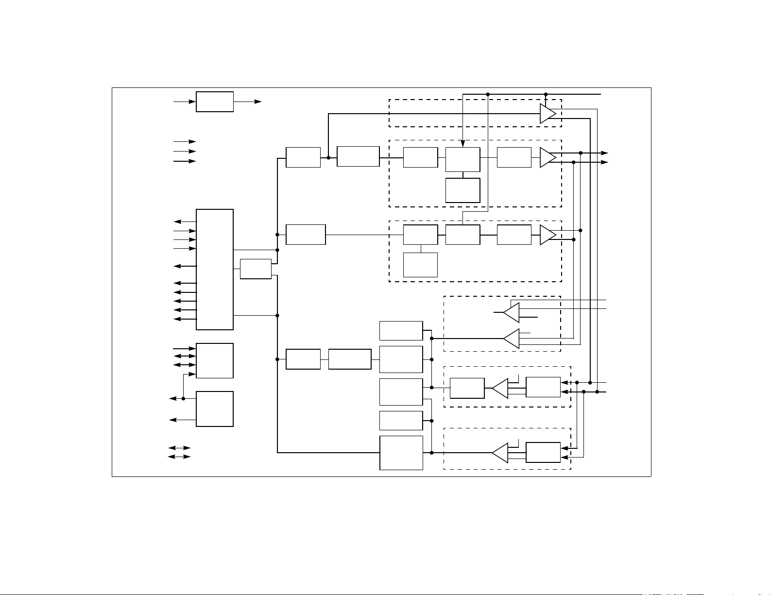
diagram is shown in Figure 1.1.
1.1.1 Channel Operation
The PHY operates in the 100BASE -TX or 100B ASE-FX mode s at 100 M bits/s, or in
the 10BASE-T mode at 10 Mbits/ s. The 100 Mbits/s mode s and the 10 Mbits/s mode
differ in data rate, signalin g protocol, and allowed wi ring as follows:
• 100BASE-TX mode uses two pairs of catego ry 5 or better UTP or STP twisted-
pair cable with 4B5B en coded, scrambled, an d MLT3 coded 62.5-MHz ter nary
data to achieve a thro ughput of 100 Mbits /s.
• The 100BASE-FX mode u ses two fiber cables with 4B 5B encoded, 125-MHz
binary data to achieve a throughput of 100 Mbits/s .
• 10 Mbits/s mode uses two pairs of category 3 or better UTP or STP twisted-pai r
cable with Mancheste r encoded 10-MHz binary data to achieve a 10 Mbits/ s
throughput
The data symbol format on the twisted-pair cable for the 100 and 10 Mbits/s modes
is defined in IEEE 80 2.3 specifications and shown in Figure 1.2.
1.1.2 Data Paths
In each device, there is a transmit data path and a receive data path associated with
each PHY channel. T he transmit data path is from the Controller Interfac e to the
twisted-pair transmitter. The receive data pa th is from the tw isted- pair r eceive r to th e
Controller Interface.
SMSC DS – LAN83C183 11 Rev. 12/14/2000
Page 12
SMSC DS – LAN83C183 12 Rev. 12/14/2000
Figure 1.1 LAN83C183 Device Block Diagram
OSCIN
RESETn
RX_EN/JAMn
RPTR
TX_CLK
TXD[3:0]
TX_EN
TX_ER/TXD4
COL
RX_CLK
RXD[3:0]
CRS
RX_DV
RX_ER/RXD4
MDC
MDINTn/MDA4n
MDIO
PLED[3:0]n
MDA[3:0]n
PLED[5:4]n
VDD[6:1]
GND[6:1]
Oscillator
Controller
Interface
(MII
or
FBI)
Serial
Port
(MI)
LED
Drivers
Collision
4B5B
Encoder
Manchester
Encoder
4B5B
Decoder
Scrambler
Descrambler
100BASE-FX Transmitter
100BASE-TX Transmitter
MLT3
Encoder
10BASE-T Receiver
ROM DAC
Clock
Generator
PLL
Squelch
Clock
& Data
Recovery
Auto-
Negotiation
& Link
Squelch
Clock & Data
Recovery
(Manchester
Decoder)
Switched
Current
Sources
Clock
Generator
PLL
100BASE-TX Receiver
100BASE-TX Receiver
MLT3
Encoder
10BASE-TX Receiver
+
+
−
+
+
−
LP
Filter
LP
Filter
+/−
+/−
+
−
+
+
−
Vth
Vth
+
-
+
-
+
−
Vth
+/−
Vth
Adaptive
Equalizer
LP
Filter
REXT
+/
FXI
TPO
TPO−/FXI
SD_THR
SD/FXDISn
TPI+/FXO
TPI−/FXO
−
+
−
+
Page 13
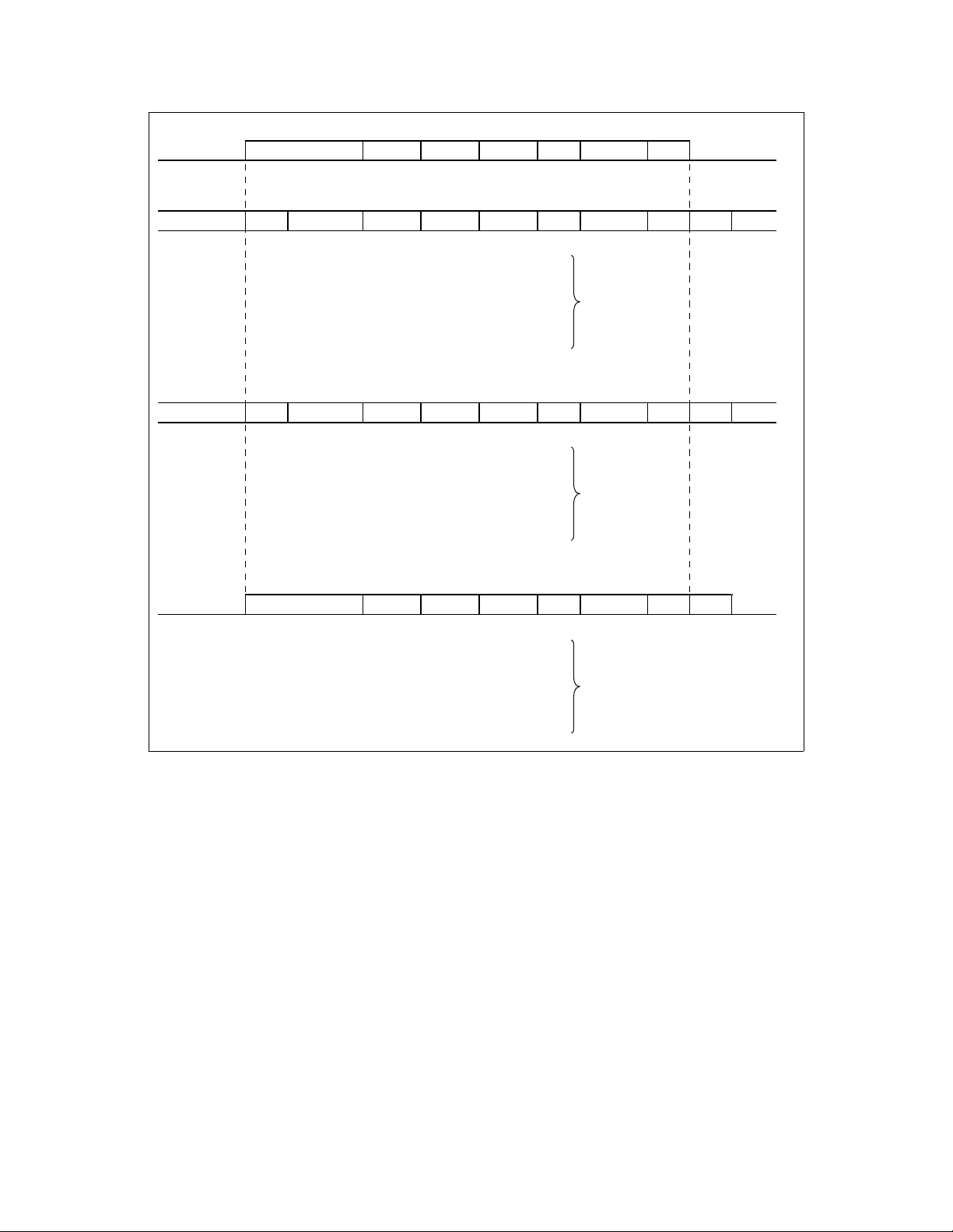
Figure 1.2 100BASE-TX /FX and 10BASE-T Frame For mat
Interframe
Gap
IDLE PREAMBLE SFD ESD IDLE
IDLE PREAMBLE SFD ESD IDLE
PREAMBLE SFD DA SA LN
SSD DA SA LN LLC DATA FCS
PREAMBLE =
DA, SA, LN, LLC D ATA, FCS =
SSD DA SA LN LLC DATA FCS
PREAMBLE =
DA, SA, LN, LLC D ATA, FCS =
Ethernet MAC Frame
100BASE-TX Data Symbols
[ 1 1 1 1 ...]
IDLE =
[ 1 1 0 0 0 1 0 0 0 1 ]
SSD =
[ 1 0 1 0 ...] 62 Bits Long
[ 1 1 ]
SFD =
[ DATA ]
[ 0 1 1 0 1 0 0 1 1 1 ]
ESD =
100BASE-FX Data Symbols
[ 1 1 1 1 ...]
IDLE =
[ 1 1 0 0 0 1 0 0 0 1 ]
SSD =
[ 1 0 1 0 ...] 62 Bits Long
[ 1 1 ]
SFD =
[ DATA ]
[ 0 1 1 0 1 0 0 1 1 1 ]
ESD =
LLC Data
Before/After
4B5B Encoding,
Scrambling, and
MLT3 Coding
Before/After
4B5B Encoding
FCS
Interframe
Gap
10BASE-T Data Symbols
IDLE PREAMBLE SFD SOI IDLE
IDLE =
PREAMBLE =
SFD =
DA, SA, LN, LLC D ATA, FCS =
DA SA LN LLC DATA FCS
[ No Transitions ]
[ 1 0 1 0 ...] 62 Bits Long
[ 1 1 ]
[ DATA ]
[ 1 1 ] With No MID Bit
SOI =
Transition
Before/After
Manchester
Encoding
SMSC DS – LAN83C183 13 Rev. 12/14/2000
Page 14
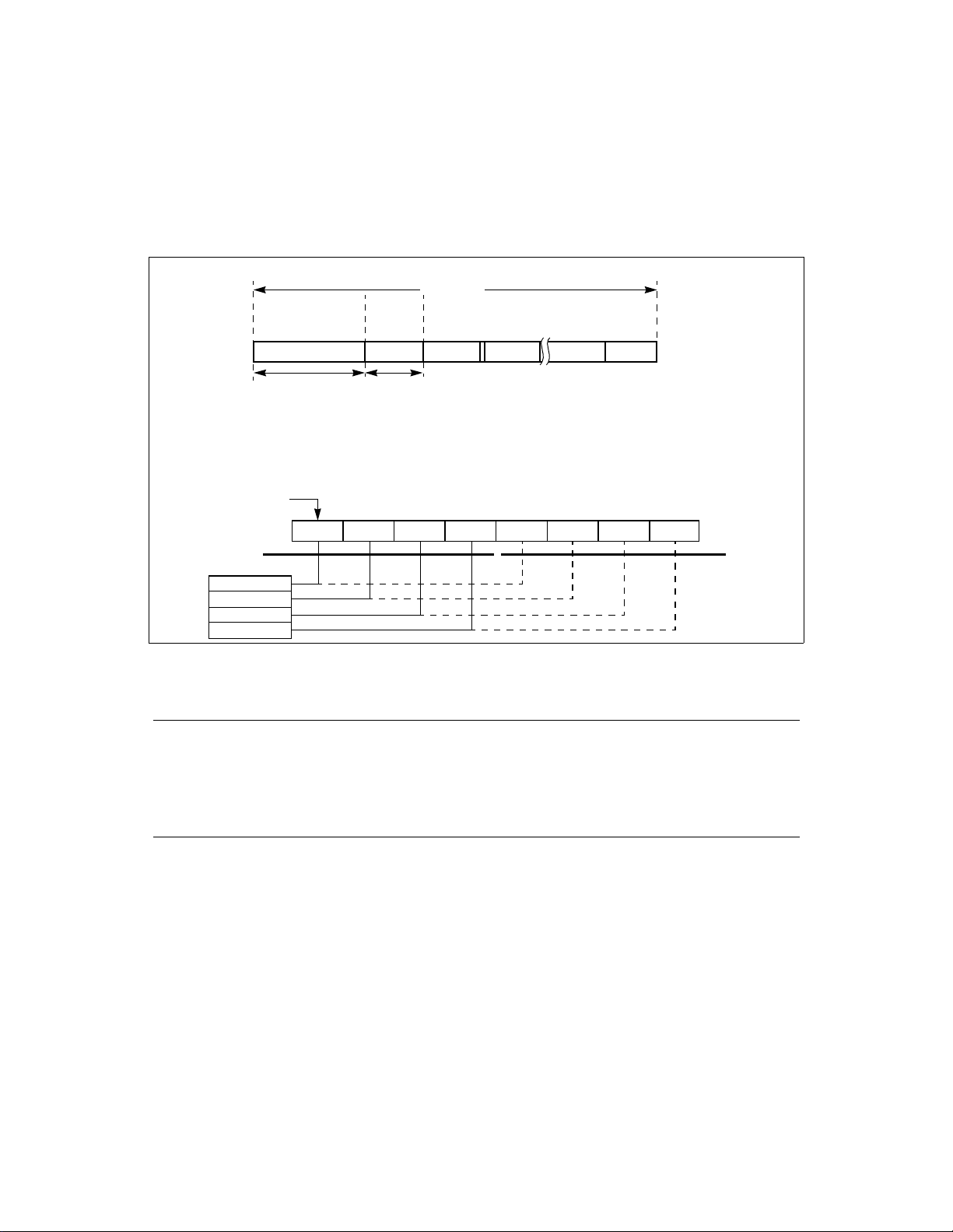
1.1.2.1 100BASE-TX
In 100BASE-TX transm it operation, data is received on th e Controller Inte rface from
an external Ethernet cont roller in the format shown in Figure 1.3 and Table 1.1. The
data is sent to the 4B5B encoder, which scrambles the encoded data. The scrambled
data is then sent to the TP tr ansm itter. The TP transmitter conv erts the enc oded an d
scrambled data into MLT 3 ternary format, presha pes the output, and drives the
twisted-pair cable.
TX_EN = 0
IDLE
First Bit
First
Nibble
TXD0/RXD0
MII
Nibble
Stream
TXD1/RXD1
TXD2/RXD2
TXD3/RXD3
Figure 1.3 MII Fram e Format
a. MII Frame Format
Start
of
PREAMBLE
PRMBLE SFD DATA 1
62 Bits 2 Bits
LSB
D0
Frame
PREAMBLE =
SFD =
DATAn =
IDLE =
b. MII Nibble Order
MAC Serial Bit Stream
D1 D2 D3 D4
TX_EN = 1
DATA Nibbles
DATA 2 DATA N-1 DATA N
[ 1 0 1 0 ...] 62 Bits Long
[ 1 1 ]
[Between 64
[TX_EN = 0]
−1518 Data Bytes]
TX_EN = 0
IDLE
D5 D6 D7
MSB
Second
Nibble
Table 1.1 Transmit Preamble and SFD Bit s at MAC Nibble Interface
Signals Bit Value
TXDO X X 1
TXD1XX0000000000000000D1D5
TXD2XX1111111111111111D2D6
TXD3XX0000000000000001D3D7
TX_EN00111111111111111111
1
11111111111111
2
3
1D0
D4
1. 1st preamb le nibble tr ansmitted.
2. 1st SFD nibble transmitted.
3. 1st data nibble transmitted.
4. D0 through D7 are the first 8 bits of the data field.
In 100BASE-TX rece ive operation, the TP r eceiver takes incom ing encoded and
scrambled MLT3 data from the twisted-pair cab le , re mov es an y hi gh -fr eq uen cy no is e
from the input, eq ualizes the inp ut signal t o compensate fo r the effects of th e cable,
performs baseline wande r correc ti on, qua li fie s the dat a with a squelc h alg or ithm, and
converts the data from MLT3-encoded levels to internal digital level s. The output of
the receiver then goes to a clock a nd data rec overy block that recover s a clock from
the incoming data, uses the clock to latch valid data into the device, and converts
the data back to NRZ form at. The 4B5B decoder and descr amb le r th en d ec odes an d
unscrambles the NRZ data, res pectively, and sends it out of the Controller Interface
4
SMSC DS – LAN83C183 14 Rev. 12/14/2000
Page 15

to an external Ether net controller. The format of the received data at the Controller
interface is as sh own in Table 1.2.
Table 1.2 Receive Pre amble and SFD Bits at MAC Nib ble Interface
Signals Bit Value
RXDO X 1
RXD1X00000000000000000D1D5
RXD2X11111111111111111D2D6
RXD3X00000000000000001D3D7
RX_DV01111111111111111111
1. First preamble nibble received. Depending on the mode, the device may eliminate either all or some
of the preamble nibbles, up to the first SFD nibble.
2. First SFD nibble received.
3. First data nibble received.
4. D0 through D7 are the first 8 bits of the data field.
1
11111111111111121D03D4
1.1.2.2 100BASE-FX
100BASE-FX oper ation is similar to 10 0BASE-TX operation except:
• The transmit output/r eceive input is not scrambled or MLT3 encoded
• The transmit data is output to a FX transmitter instead of the TP waveshaper/
transmitter
• The receive data is inp ut to the FX ECL level dete ctor instead of the equali zer
and associated T P circuitry
• The FX Interface has a signal detect input
4
1.1.2.3 10BASE-T
10BASE-T operation is similar to the 100B ASE-TX operation exce pt:
• There is no scrambler /descrambler
• The encoder/decode r is Manchester inst ead of 4B5B
• The data rate is 10 M bits/s instead of 100 M bits/s,
• The twisted-pair s ymbol data is two-leve l Manchester instead of ternary MLT-3.
• The transmitter generates link pulses during the idle period
• The transmitter de tects the jabber conditi on
• The receiver detects l ink pulses and implements th e AutoNegotiation algor ithm
SMSC DS – LAN83C183 15 Rev. 12/14/2000
Page 16

1.2 BLOCK DIAGRAM DESCRIPTION
The LAN83C183 PHY dev ice has the following main b locks:
• Oscillator and Clock
• Controller Interface
• 4B5B/Manchester En coder/Decoder
• Scrambler/Descrambler
• Twisted-Pair Transmitters
• Fiber Transmitter
• Twisted-Pair Receivers
• Fiber Receiver
• Clock and Data Recovery
• AutoNegotiation/Link I ntegrity
• Descrambler
• Collision Detection
• LED Drivers
A Management Interfa ce (MI) serial port prov ides access to 11 internal PHY
registers.
Figure 1.1 sh ows the main bloc ks, along with the ir associated signals. The fo llowing
sections describe each of the blocks in Figure 1.1. The perfo rmance of the device in
both the 10 and 100 Mbi ts/s modes is descri bed.
1.2.1 Oscillator and Clock
The LAN83C183 requir es a 25 MHz reference f requency for internal si gnal
generation. This 25 MHz refer ence freq uency is genera ted with ei ther an ex ternal 25
MHz crystal connecte d between OSCIN and GND or w ith the application of an
external 25-MHz clock to OSCIN.
The device provides eit her a 2.5-MHz or 25-MHz refer ence clock at the TX_CLK or
RX_CLK output pins f or 10-MHz or 100-MHz o peration, respectivel y.
1.2.2 Controller Interface
This section desc ribes the controller inter face operation. The LA N83C183 has two
interfaces to an exte rnal controller:
• Media Independent Int erface (MII)
• Five Bit Interface (FBI)
1.2.2.1 MII INTERFACE
The device has an M II interface to an external E thernet Media Access Cont roller
(MAC).
MII (100 Mbits/s) – The MII is a nibble wide packet dat a interface defined in IEEE
802.3 and shown in Figure 1.3. The LAN83C183 mee ts all the MII requireme nts
outlined in IEEE 802.3 . The LAN83C183 can dire ctly connect, without any external
logic, to any Ethern et controller or other devi ce that also complies wi th the IEEE
802.3 MII specificati ons.
SMSC DS – LAN83C183 16 Rev. 12/14/2000
Page 17

The MII interface co ntains the following sign als:
• Transmit data bits (TXD[3:0])
• Transmit clock (TX _CLK)
• Transmit enable (TX_EN)
• Transmit error (TX_ER)
• Receive data bits (RXD[3 :0])
• Receive cloc k (RX_CLK)
• Carrier sense (CRS)
• Receive data valid (RX _DV)
• Receive data error (RX_ER)
• Collision (COL)
The transmit and re ceive clocks operate a t 25 MHz in 100 Mbits/s mode.
On the transmit side, the TX_CLK output runs continuously at 25 MHz. When no data
is to be transmit ted, TX_EN must be deass erted. While TX_EN is dea sserted,
TX_ER and TXD[3:0] are ignored and no data is cl ocked into the device. Whe n
TX_EN is asserted on the rising edge of TX_CLK, data on TXD[3:0] is clocked into
the device on the risin g edge of the TX_CLK output c lock. TXD[3:0] input da ta is
nibble wide packet data whos e format must be the sam e as specified in IEEE 802.3
and shown in Figure 1.3. When a ll data on TXD[3:0] has been l atched into the
device, TX_EN must be deasserted on the rising e dge of TX_CLK.
TX_ER is also clocked in on the rising edge of TX_CLK. TX_ER is a trans mit error
signal. When th is signal is asserted, the device substitutes an er ror nibble in place
of the normal data nibble that was clocked in on TXD[3: 0]. The erro r nib ble is defined
to be the /H/ symbol, whic h is defined in IEEE 80 2.3 and shown in Table 1.3.
SMSC DS – LAN83C183 17 Rev. 12/14/2000
Page 18

Ta ble 1.3 4B/5B Symbol Mapping
Symbol
Name Description 5B Code 4B Code
0 Data 0 0b11110 0b0000
1 Data 1 0b01001 0b0001
2 Data 2 0b10100 0b0010
3 Data 3 0b10101 0b0011
4 Data 4 0b01010 0b0100
5 Data 5 0b01011 0b0101
6 Data 6 0b01110 0b0110
7 Data 7 0b01111 0b0111
8 Data 8 0b10010 0b1000
9 Data 9 0b10011 0b1001
A Data A 0b10110 0b1010
B Data B 0b10111 0b1011
C Data C 0b11010 0b1100
D Data D 0b11011 0b1101
E Data E 0b11100 0b1110
F Data F 0b11101 0b1111
I Idle 0b11111 0b0000
J SSD #1 0b11000 0b0101
K SSD #2 0b10001 0b0101
T ESD #1 0b01101 0b0000
R ESD #2 0b00111 0b0000
H Halt 0b00100 Undefined
1
– Invalid codes All others
1. These 5B codes are not used. The decoder decodes these 5B codes to
4B 0000. The encoder encodes 4B 0000 to 5B 11110, as shown in symbol
Data 0.
0b0000*
Because the OSCIN in put clock generates the TX_CLK output clock, the T XD[3:0],
TX_EN, and TX_ER sig nals are also clocked i n on rising edges of OSCIN.
On the receive side, a s lon g as a val id dat a pa ck et i s not d etected, CRS and RX_DV
are deasserted and the RXD[3:0] sig nals are held L OW. When the start of pack et is
detected, CRS and RX_ DV are asserted on the fal ling edge of RX_CLK. The
assertion of RX_DV indicates that valid data is clocked out on RXD[3:0] on the falling
edge of the RX_CLK. The R XD[3:0] data has the same frame structure as the
TXD[3:0] data and is specified in IEE E 80 2.3 an d sho wn in Figure 1.3. When the end
SMSC DS – LAN83C183 18 Rev. 12/14/2000
Page 19

of the packet is detec ted, CRS and RX_DV are deas serted, and RXD[3:0] is hel d
LOW. CRS and RX_DV also stay deasser ted if the device is in the L ink Fail State.
RX_ER is a receive erro r output tha t is as serte d when ce rtain errors ar e detec ted on
a data nibble. RX_ER i s asserted on the falling edge of RX_ CLK for the duratio n of
that RX_CLK clock cyc le during which the nibble c ontaining the error is ou tput on
RXD[3:0].
The collision output, COL, is asserted whenev er the collision cond ition is detected.
MII (10 Mbits/s) – MII 10 Mbits/s operation is identical to 100 Mbits/s operation except:
• The TX_CLK and RX_CLK c lock frequency is reduc ed to 2.5 MHz
• TX_ER is ignored
• RX_ER is disable d and always held LOW
• Receive operation is modified as follows:
On the receive side, w hen the squelch circuit d etermines that invalid data is
present on the TP in puts, the receiver is id le. During idle, RX_CLK follows
TX_CLK, RXD[3:0] is held LOW, and CRS and RX_DV are dea sserted. When a
start of packet is d etected on the TP receive i nputs, CRS is asserted and the
clock recovery pr ocess starts on the i ncoming TP input data. After the receive
clock has been recov ered from the data, the RX_ CLK is switched over to the
recovered clock an d the data valid signal RX_DV is asserted on a falling e dge
of RX_CLK. Once RX_DV is asse rted, valid data is clocked out on RXD [3:0] on
the falling edge of RX_CL K. The RXD[3:0] data has the same packet structure
as the TXD[3:0] data and is formatted on RXD[3:0] as specified in IEEE 802.3
and shown in Figure 1.3. When the end o f packet is detect ed, CRS and RX_DV
are deasserted. CR S and RX_DV also stay deasserted as long as the devic e is
in the Link Fail Sta te.
1.2.2.2 FBI INTERFACE
The Five Bit Interface (als o referred to as FBI) is a five- bit wide interface that is
produced when the 4B 5B encoder/decoder is b ypassed. The FBI is prim arily used
for repeaters or Ethe rnet controllers that hav e integrated encoder/dec oders.
The FBI is identical to the MII except:
• The FBI data path is fiv e bits wide, not nibble wid e like the MII
• The TX_ER pin is recon figured to be the fifth transm it data bit (TXD4)
• The RX_ER pin is reco nfigured to be the fifth recei ve data bit (RXD4)
• CRS is asserted as long as the device is i n the Link Pass State
• COL is not valid
• RX_DV is not valid
• The TX_EN pin is ignored
There is no FBI operati on in the 10 Mbits/s mode.
1.2.2.3 SELECTION OF M II OR FBI
FBI Selection – The FBI is automa tical ly enab led when the 4B 5B en coder/ deco der is
bypassed. Bypassing the encoder/decoder passes the 5B symbols between th e
receiver/transm itter directly to the FBI without any alterations o r substitutions. To
SMSC DS – LAN83C183 19 Rev. 12/14/2000
Page 20

bypass the 4B5B encoder/decoder, set the Bypass Encoder bit (BYP_ENC) in the MI
serial port Configu ration 1 register.
When the FBI is enab led, it may also be des irable to bypass the
scrambler/descr ambler and disable the internal CRS loopbac k function. To bypass
the scrambler/descramb le r, set the Bypass Scramb ler bit (BYP_SCR) in the MI ser ia l
port Configuration 1 r egister. To disable the internal CRS loopback, set the TX_E N
to CRS loopback disab le bit (TXEN_CRS) in the MI serial port Configura tion 1
register.
MII Selection – To disable the MII (and FBI) in puts and outpu ts, set the MII_DIS bi t in
the MI serial por t Control register. When the MII is disabled, the MII an d FBI inputs
are ignored, and the MII, FBI, and TPI outputs ar e place d in a high-im pedanc e state.
The MII pins affected are:
• RX_CLK
• RXD[3:0]
• RX_DV
• RX_ER
• COL
If the MI address line s, MDA[4:0]n, are pulled HIGH during reset or poweru p, the
LAN83C183 powers up and resets with the MII and FBI d isabled. Otherwise, the
LAN83C183 powers up and resets with the MII and FBI e nabled.
In addition, when the R/ J_CFG bit in the MI serial port Configuration 1 re gister is
LOW, the RX_EN/JAMn pin is configu red for RX_EN ope ration. If the RX_E N pin is
LOW in this situation, the MII controller inter face outputs are placed in the highimpedance state.
1.2.3 Encoder
This section descr ibes the 4B5B e ncoder, which is used in 100 Mbi ts/s operatio n. It
also describes the Ma nchester Encoder, used in 10BASE-T oper ation.
1.2.3.1 4B5B ENCODER (10 0 MBITS/S)
100BASE-TX ope ration requires that the d ata be 4B 5B en co ded. The 4B5B Encoder
block shown in Figure 1.1 converts the four-bit da ta nibbles into five-bit data words.
The mapping of the 4 B nibbles to 5B codew ords is specified in IEE E 802.3 and is
shown in Table 1.4.
SMSC DS – LAN83C183 20 Rev. 12/14/2000
Page 21

Table 1.4 4B/5B Symbol Mapping
Symbol Name Description 5B Code 4B Code
0 Da t a 0 1111 0 00 0 0
1 Data 1 01001 0001
2 Data 2 10100 0010
3 Data 3 10101 0011
4 Data 4 01010 0100
5 Data 5 010 11 0101
6 Data 6 01110 0110
7 Da t a 7 0 1111 0 111
8 Data 8 10010 1000
9 Data 9 100 11 1001
A Data A 10110 1010
B Da t a B 10 111 1 0 11
C Data C 11010 1100
D Data D 11011 1101
E Data E 111 00 1110
F D a t a F 1110 1 1111
I Idle 11111 0000
J SSD #1 11000 0101
K SSD #2 10001 0101
T ESD #1 01101 0000
R ESD #2 00111 0000
H Halt 00100 Undefined
1
--- Invalid codes All others
1. These 5B codes are not used. The decoder converts them
to a 4B code of 0000. The encoder converts the 4B 0000
co d e t o t h e 5 B 1111 0 c od e , a s s h o w n i n sy m b o l 0 .
0000
The 4B5B encoder takes 4B (four-bit) nibbles from the Transmit MAC block, converts
them into 5B (five-bit) words accordin g to Table 1.4, a nd sends the 5B words to the
scrambler. The 4B5B encoder also substitutes the first eight bits of the preamble with
the Start of Stream Del imiter (SSD) (/J/K/ symb ols) and adds an End of S tream
Delimiter (ESD) (/T/R/ symb ols) to the end of each pack et, as defined in IE EE 802.3
and shown in Figure 1.2. The 4B5 B encoder also fills t he period between packets
(idle period), with a c ontinuous stream of idl e symbols, as shown in Figure 1.2.
1.2.3.2 MANCHESTER ENCODER (10 MBITS/S)
The Manchester Enc oder shown in Figure 1.1 is used for 10 Mbits/s operation. It
combines clock and non-retu rn to zero inverte d (NRZI) data suc h that the first half of
SMSC DS – LAN83C183 21 Rev. 12/14/2000
Page 22

the data bit contains the c ompleme nt of the data, a nd the second half of the da ta bit
contains the true data , as specified in IEEE 802.3. This process guar antees that a
transition always oc curs in the middle o f the bi t cell . The Ma nches ter en coder o n the
device converts the 10 Mbits/s NRZI data from the Ethernet co ntroller interface into
a single data stream for the T P tran smitter and adds a start of id le puls e (S OI) at the
end of the packet as sp ecified in IEEE 802.3 and shown in Figure 1.2. The
Manchester encodin g process is only do ne on actual packet data; du ring the idle
period between packe ts, no signal is transm itted except for period ic link pulses.
1.2.3.3 ENCODER BYPASS
Setting the Bypass Encoder/Decoder bit (BYP_ENC) in the MI serial port
Configuration 1 regis ter bypasses the 4B5B encoder. When this bit is set, 5B code
words are passed directly from the c ontroller interface to the scrambler without any
of the alterations described in Section 1.2.3 .1, “4B5B Encoder (100 Mbits/s ),”
page 1-20. S etting the bit automatically places the device in the FBI mode as
described in the subsection entitled “FB I Selection” on page 1-19.
1.2.4 Decoder
This section desc ribes the 4B5B decode r, used in 100 Mbits/s operation, whic h
converts 5B encoded data to 4B nib bles. It also describes th e Manchester D ecoder,
used in 10BASE-T oper ation.
1.2.4.1 4B5B DECODER (10 0 MBITS/S)
Because the TP inp ut data is 4B5B encode d on the transmi t side, th e 4B5B decod er
must decode it on the r eceive side. The mapping of the 5B codewords to the 4 B
nibbles is specifi ed in IEEE 802.3. T he 4B5B dec oder takes th e 5B codewords f rom
the descrambler, converts them int o 4B nibbles according to Table 1.4, and s ends
the 4B nibbles to the r eceive Ethernet contr oller.
The 4B5B decoder also strips off the SSD delimiter (/J/K/ symbols), and replaces it
with two 4B Data 5 nibb les (/5/ symbol). It also strips off the ESD delimiter (/T /R/
symbols), and rep laces it with two 4B Data 0 nibb les
(/I/ symbol), per IEEE 8 02.3 specifications (see Figure 1.2).
The 4B5B decoder detec ts SSD, ESD, and codeword er rors in the incoming dat a
stream as specifi ed in IEEE 802.3. To indicate these errors, the device asser ts the
RX_ER output as well as the SS D, ESD, and CWRD bits in the MI seria l port Status
Output register while the errors are being transm itted across RXD[3:0 ].
1.2.4.2 MANCHESTER DECODER (10 MBITS/S)
In Manchester coded data, the first half of the data bit contains the com plement of
the data, and the s econd half of the da ta bit contains the true dat a. The M ancheste r
Decoder converts the s ing le data str ea m from the TP receiver into n on- retur n to z ero
(NRZ) data for the cont roller interface. To do this, it decodes the data and s trips off
the SOI pulse. Becau se the Clock and Data Recovery bloc k has already s eparated
the clock and data fr om the TP receiver, that block inherentl y performs the the
Manchester deco ding.
1.2.4.3 DECODER BYPASS
Setting the Bypass Encoder/Decoder bit (BYP_ENC) in the MI serial port
Configuration 1 regis ter bypasses the 4B5B decoder. When this bit is set, 5B code
words are passed directly to the controller interface from the descrambler without any
of the alterations described in Sect ion 1.2.4, “Decoder,” page 1-22. Additionally, the
SMSC DS – LAN83C183 22 Rev. 12/14/2000
Page 23

CRS pin is continuous ly asserted whenever the device is in the Link P ass state.
Setting the bit autom atically places the devi ce in the FBI mode as des cribed in the
subsection entitled “FBI Selection” on page 1-19.
1.2.5 Scrambler
100BASE-TX tran smission requi res scramblin g to reduce the radi ated emission s on
the twisted pair. The scrambler takes the NRZI encoded data from the 4B5B encoder,
scrambles it per the IEEE 8 02.3 specific ations, and se nds it to the TP transmitter. A
scrambler is not used for 10 Mbits/s oper ation.
1.2.5.1 SCRAMBLER BYPASS
Setting the Bypass Encoder/Decoder bit (BYP_SCR) in the MI serial port
Configuration 1 register bypasses the scrambler. When this bit is set, 5B data
bypasses the scramb ler and goes directly to the 100BASE-TX trans mitter.
1.2.6 Descrambler
The descramble r block shown in Figure 1.1 is us ed in 100BASE-TX operati on. The
device descrambler tak es the scrambled NRZI data from the data recovery block,
descrambles it acco rding to IEE E 802.3 specifi cations , alig ns the data on t he corr ect
5B word boundaries, and sends it to the 4B5B decoder.
The algorithm for sync hronization of the descr ambler is the same as the algorithm
outlined in the IEE E 802.3 specificatio n.
After the descrambl er is synchronize d, it maintains synchr onization as long as
enough descrambled idle pattern ones are det ected within a given i nterval. To st ay
in synchronizati on, the descrambler nee ds to detect at least 25 consecutive
descrambled idle patte rn ones in a 1 ms interv al. If 25 consecuti ve descram bled idle
pattern ones are not d etected within the 1 ms interval, the descram bler goes out of
synchronization and restarts the synch ronization process.
If the descrambler i s in the unsynchronized state, the descrambl er Loss of
Synchronization D etect bit (LOSS_SYNC) is s et in the MI serial port S tatus Output
register. The bit stays set until t he descrambler achie ves synchronization.
The descrambler is disabled for 10BAS E-T operation.
1.2.6.1 DESCRAMBLER BYPASS
Setting the Bypass Encoder/Decoder bit (BYP_SCR) in the MI serial port
Configuration 1 regis ter bypasses the des crambler. When this bit is set, 5B data
bypasses the descra mbler and goes directly f rom the
100BASE-T rece iver to the 4B5B decoder.
SMSC DS – LAN83C183 23 Rev. 12/14/2000
Page 24

1.2.7 Twisted-Pair Transmitters
This section desc ribes the operation of t he 10 and 100 Mbits/s TP transmitters.
1.2.7.1 100 MBITS/S TP TRANSMITTER
The TP transmitter co ns ists of an M LT3 encoder, waveform generator, and line driver.
The MLT3 encoder converts the NRZI data from the scrambler into a three-level code
required by IEEE 802.3 . MLT3 coding uses three l evels, converting ones t o
transitions between the three le vels, and z eros to no tr ansitions or changes i n level.
The purpose of the wavefo rm generator is to sha pe the transmit output puls e. The
waveform generator tak es the MLT3 three level encoded waveform and uses a n
array of switched c urrent sources to c ontrol the shape of the tw isted-pair output
signal. The wave form generator consists of switched curren t sources, a clock
generator, filter, and logic. The switched current sources contr ol the rise and fall time
as well as signal l evel to meet IEEE 802.3 req uirement s. The output of t he switc hed
current sources goe s through a second orde r low-pass filter that “smooths” the
current output and removes any high-fr equency components. In this way, the
waveform generator preshapes the output waveform transmitted onto the twisted-pair
cable such that the wav eform meets the pulse templ ate requirements outlined i n
IEEE 802.3. The waveform genera tor eliminates the need for an y external fi lters on
the TP transmit output.
The line driver c onverts the shap ed and smoot hed waveform to a c urrent output that
can drive greater than 100 meters of category 5 uns hi eld ed twisted-pair cable or 1 50ohm shielded twisted- pair cable.
1.2.7.2 10 MBITS/S TP TRANSMITTER
Even though the 10 Mbits /s transmitter operation is m uch different than that of 100
Mbits/s, it also con sists of a waveform gene rator and line driver ( see Figure 1.1).
The waveform generator, which consists of a ROM, DAC, clock generator, and filter,
shapes the output tr an sm it pul se . T he DAC gen er ates a stair-stepped repre se ntat ion
of the desired output waveform. The stairstepped DAC output then is passed through
a low-pass filter to “smooth” the DAC outpu t and remove any high-fre quency
components. The DAC va lues are determined fr om the data at the ROM addres ses.
The data is chosen to shape the pulse to the desired templ ate. The clock generato r
clocks the data into the DAC at high speed. In this way, the waveform generat or
preshapes the output wave form to be tra nsmitted on to the twis ted-p air cable to me et
the pulse template r equirements outlined i n IEEE 802.3 Clause 14 and shown in
Figure 1.4 an d Table 1.5. The waveshaper replaces and el imi na tes ex ter na l filte rs on
the TP transmit output.
The line driver c onverts the shap ed and smoot hed waveform to a c urrent output that
can drive greater than 100 meters of category 3/4/5 100- o hm un shi el ded twis ted -p air
cable or 150-ohm s hielded twisted-pair cabl e without any external fi lters.
During the idle period, no output signals are tran smitted on the TP outputs ex cep t for
link pulses.
SMSC DS – LAN83C183 24 Rev. 12/14/2000
Page 25

Figure 1.4 TP Output Voltage Template
T
Voltage (V)
1.0
0.8
0.6
0.4
0.2
0.0
- 0.2
- 0.4
- 0.6
- 0.8
- 1.0
A
0102030405060708090100110
B
D
C
E
Time (ns)
H
F
G
I
M
Table 1.5 TP Outpu t Vo ltage - 10 Mbits/s
Reference Time (ns) Internal MAU Voltage (V)
L K
N
P
O
Q
J
W
R
S
U
V
T
A0 0
B15 1.0
C15 0.4
D25 0.55
E32 0.45
F39 0
G57 −1.0
H48 0.7
I67 0.6
J89 0
K74 −0.55
L73 −0.55
M61 0
N85 1.0
O100 0.4
P 110 0.75
Q 111 0.15
R 111 0
SMSC DS – LAN83C183 25 Rev. 12/14/2000
Page 26

Table 1.5 TP Output Voltage - 10 Mbits/s (Cont.)
Reference Time (ns) Internal MAU Voltage (V)
S 111 −0.15
T110 −1.0
U100 −0.3
V110 −0.7
W90 −0.7
1.2.7.3 TRANSMIT LEVEL ADJUST
The transmit output c urrent level is deriv ed from an internal refe rence voltage and
the external resisto r on the REXT pin. The trans mit leve l can be adjusted with either :
• The external resis tor on the REXT pin, or
• The four Transmit Level Adjus t bi ts (T LVL[3:0]) in the MI serial p ort Conf igu ra tio n
1 register as shown in Table 1.6. The adjustment range is approx imately -14%
to +16% in 2% steps.
Table 1.6 Transmit Level Adjust
TLVL[3:0]
Bits Gain
0000 1.16
0001 1.14
0010 1.12
0011 1.10
0100 1.08
0101 1.06
0110 1.04
0111 1.02
1000 1.00
1001 0.98
1010 0.96
1011 0.94
1100 0.92
1101 0.90
1110 0.88
1111 0.86
SMSC DS – LAN83C183 26 Rev. 12/14/2000
Page 27

1.2.7.4 TRANSMIT RISE AND FALL TIME ADJUST
The transmit output ri se and fal l t ime c an b e ad jus te d wi th th e two Transmit Rise/ F all
time adjust bits (TRF[1:0]) in the MI serial port Configuration 1 register. The
adjustment range is
−0.25 ns to +0.5 ns in 0.25 ns steps.
1.2.7.5 STP (150 OHM) CABLE MODE
The transmitter can b e configured to drive 15 0 Ω shielded twisted-pair cable. To
enable this configurati on, set the Cable Type Select bit (CABLE) in the MI serial port
Configuration 1 regis ter. When STP mode is enabled, the ou tput current is
automatically ad justed to comply with IEE E 802.3 levels.
1.2.7.6 TRANSMIT ACTIVITY INDICATION
Appropriately setting the programmable LED Output Sel ect bits in the MI serial port
LED Configuration 2 re gister programs trans mit activity to appear on s ome of the
PLED[5:0]n pins. When one or more of t he PLE D[5:0]n p ins is program med to b e an
activity or transmit a ctivity detect outpu t, that pin is asserted LOW for 100 ms eve ry
time a transmit pa cket occurs. The PLED[5:0]n outp uts are open-drain with resistor
pullup and can driv e an LED from V
1.2.14, “LED Drivers,” page 1-36 for more detailed i nformation on the LED output s.
1.2.7.7 TRANSMIT DISABLE
Setting the Transmit Disable bi t (XMT_DIS) in the MI se rial port Configuration 1
register disables the TP trans mitter. When the bit is set, the TP transmitter is forced
into the idle state, n o data is t ransmitted, no link p ulses are transmitted , and inter nal
loopback is disab led.
or can drive othe r digital inpu ts. See Section
DD
1.2.7.8 TRANSMIT POWERDOWN
Setting the Transmit Powerdown b it (XMT_PDN) in the MI serial p ort Configuration
1 register powers down the TP transmitte r. When the bit is set, the TP transm itter is
powered down, the TP tr ansmit outputs are high impedance, and the rest of the
LAN83C183 operates normall y.
1.2.8 Twisted-Pair Receivers
The device is capabl e of operating at either 10 - or 100-Mbits/s. This section
describes the twisted-pa ir receivers and squelc h operation for both modes of
operation.
1.2.8.1 100 MBITS/S TP RECEIVE R
The TP receiver de tects input si gnals from the twi sted-pair inpu t and converts them
to a digital data bit stream ready for clock and data recovery. The receiver can
reliably detect 100BASE-TX compliant transmitter data that has been passed through
0 to 100 meters of
Ω category 5 UTP or 150-ohm STP cable.
100
The 100 Mbits/s rec eiver consists of an adaptive equalizer, baseline wander
correction circuit, c omparators, and an MLT3 decoder. The TP inputs first go to an
adaptive equalizer. The adaptive equal izer compensates for the low-pass
characteristics of the cable, and can adapt and compensate for 0 to 10 0 meters of
category 5, 100-ohm o r 150-ohm STP cable. T he baseline wander correction circuit
restores the DC compone nt of the input waveform th at the external transforme rs
have removed. The com parators convert the e qualized signal back to digital levels
and qualify the data with th e squel ch circ uit. T he MLT3 decoder takes the three- leve l
SMSC DS – LAN83C183 27 Rev. 12/14/2000
Page 28

MLT3 encoded outpu t data from the comparator s and converts it to nor mal digital
data to be used for clock and data recovery.
1.2.8.2 10 MBITS/S TP RECEIVER
The 10 Mbits/s rece iver detects input signa ls from the twisted-pai r cable that are
within t h e te m pl a te sh o w n i n Figure 1.5 The TP inputs are biased by internal resistors
and go through a low-pa ss filter designed to e liminate any high-freq uency input
noise. The output of the receive filter goes t o two different types of comparator s:
squelch and zero c rossing. The squelch comp arator determines wheth er the signal
is valid, and the zero crossing comparator senses the actual data transitions after the
signal is determin ed to be valid. The out put of the squelch comparator goes to the
squelch circuit and is also used fo r link pulse detec tion, SOI detection, and reverse
polarity detection. T he output of the zero-crossi ng comparator is used for clock and
data recovery in the M anchester decoder.
Figure 1.5 TP Input Voltage Template (10 Mbits/s)
0 PW/4 3PW/4 PW
1.2.8.3 SQUELCH (100 MBITS/S)
The Squelch block determines if the TP inpu t contains valid data. T he 100 Mbits/s
TP squelch is one of th e criteria used to deter mine link integrity. The squelch
comparators compa re the TP inputs agains t fixed positive and nega tive thresholds,
called squelch lev els. The output from the squelch comparat or goes to a digital
squelch circuit, which d eter mines whether the rec ei ve inpu t data on that po rt i s vali d.
If the data is invalid , the receiver is in th e squelched state. If the in put voltage
exceeds the squelch levels at least fou r times with a lternating p olarity within a 10
interval, the squel ch circuit det ermines that th e data is valid a nd the receiv er enters
into the unsquelch state.
Short Bit
Slope 0.5 V/ns
585 mV sin (π ∗ t/PW)
0PW
Long Bit
Slope 0.5 V/ns
585 mV sin (
585 mV sin[2
π ∗ t/PW)
π (t − PW2)/PW)]
3.1 V
585 mV
3.1 V
585 mV
µs
In the unsquelch state, the receive thres hold level is re duced by approxim ately 30%
for noise immunity reasons and is called the unsquelch level. When the receiver is
in the unsquelch stat e, the input signal is considered valid.
SMSC DS – LAN83C183 28 Rev. 12/14/2000
Page 29

The device stays in the unsquelch state un til loss of data is detec ted. Loss of data
is detected if no alter nating polarity unsque lch trans ition s are de tected during any 10
µs interval. When a l oss of data is detected, the receive squelc h is turned on again .
1.2.8.4 SQUELCH (10 MBITS/S)
The TP squelch algo rithm for 10 Mbits/s mod e is identical to the
100 Mbits/s mode, except:
• The 10 Mbits/s TP squelch algorithm is not used for link integrity, but to sense
the beginning of a pa cket
• The receiver goes into the unsquelch state if the input voltage exceeds th e
squelch levels for three bit times with altern ating polarity within a 50 to 250 ns
interval
• The receiver goes i nto the squelch state w hen SOI is detected
• Unsquelch detection h as no effect on link integr ity (link pulses are u sed in 10
Mbits/s mode for that p urpose)
• Start of packet is de termined when the receiv er goes into the unsq uelch state
and CRS is asserted
• The receiver meets the s quelch requirements defi ned in IEEE 802.3 Clause 14.
1.2.8.5 EQUALIZER DISABLE
Setting the Equali zer Disable bit (EQLZR) in th e MI serial port Configu ration 1
register disables th e adaptive equaliz er. When disabled, the equalizer is for ced into
the response it would normally have if zer o cable length was detecte d.
1.2.8.6 RECEIVE LEVEL ADJUST
Setting the Receiv e Level Adjust bit (RLV0) in the MI serial po rt Configuration 1
register lowers the receiver squelch and unsquelch level s by 4.5 dB. Setting this bit
may allow the device to support longer cabl e lengths.
1.2.8.7 RECEIVE ACTIVITY INDICATION
Appropriately settin g the programmable LED ou tput select bits in the MI s erial port
LED Configuration 2 re gister programs receiv e activity to appear on so me of the
PLED[5:0]n pins. When one or more of the PLED[5:0]n pins is programmed to be a
receive activity or activity detect output, that pin is asserted LOW for 100 ms every
time a receive p acket occurs. The PLED[ 5:0]n outputs are open- drain with resistor
pullup and can drive a n LE D from V
1.2.14, “LED Drivers,” page 1-36 for more detailed i nformation on the LED output s.
1.2.9 FX Transmitter and Receiver
The FX transmitter and receiver implement the 100BASE-FX function defined in IEEE
802.3. 100BASE-FX is intended for transmission and reception of data over fiber and
is specified to oper ate at 100 Mbits/s. Th us, the FX transmitter and receiver in the
device only operat e when the device is pl aced in 100 Mbits/s m ode.
1.2.9.1 TRANSMITTER
The FX transmitter converts data fr om the 4B5B encoder into binary NRZI data and
outputs the data onto t he FXO+/- pins. The output dri ver is a differential current
source that is abl e to dr ive a 100
drive an external fibe r optic transceiver. The FX transmitter meets all the
requirements defined i n IEEE 802.3.
or can drive another digi tal input. S ee Section
DD
Ω load to ECL lev els. The FX O+/- p ins can direct ly
SMSC DS – LAN83C183 29 Rev. 12/14/2000
Page 30

1.2.9.2 RECEIVER
The FX transmit output current level is derived from an internal reference voltage and
the external resistor on the REXT pin. The FX tra nsmit level can be adju sted with
this resistor or it can also be adjusted w ith the two FX Transmit Level Ad just bits
(FXLVL[1:0]) in the MI serial port Mask r egister as shown in Table 1.7.
Table 1.7 FX Transmit Level Adjust
FXLVL[1:0]
Bits Gain
11 1.30
10 1.15
01 0.85
00 1.00
The FX receiver:
• Converts the differential EC L inputs on the FXI+/- pi ns to a digital bit stre am
• Validates the data o n FXI+/- with the SD/FXDIS n input pin
• Enable or disables the FX interface with the SD/F XDISn pin.
The FX receiver meets all requirements defi ned in IEEE 802.3.
The input to the FXI+/- pins can be directly dr iven from a fiber opti c transceiver a nd
first goes to a comparator. The comparator co mpa res the inpu t wav eform agai ns t the
internal ECL threshold levels to produce a low jitter serial bit stream with internal logic
levels. The data fr om the comparator output i s then passed to the cloc k and data
recovery block, pr ovided that the signal detect input, SD/FXDISn, is asserted.
Signal Detect – The FX r eceiver has a signal de tect input pin, SD/FXDISn , which
indicates whether the incoming da ta on FXI+/- is valid or not. Th e SD/FXDISn inpu t
can be driven dire ctly from an external fibe r optic transceiver and me ets all
requirements define d in the IEEE 802.3 specific ations.
The SD/FXDISn input goe s directly to a com parator. The comparator compares the
input waveform agains t the internal ECL threshol d level to produce a digital signal
with internal logi c le ve ls . T h e o utpu t o f the signal det ect c om par ato r the n goes to the
link integrity and squelch blocks. If t he SD/FXDISn input is asserted, the device i s
placed in the Link Pass state and the input data on FXI+/- is determined to be vali d.
If the SD/FXDISn input i s deasserted, t he device is plac ed in the Link F ail state and
the input data on FXI+ /- is determined to be in valid.
The SD_THR pin adjus ts the ECL trip point of the SD/FXDISn input. When the
SD_THR pin is tied to a v oltage between GND and GN D + 0.45V, the trip point of
the SD/FXDISn ECL inp ut buffer i s inter nally s et to V DD
− 1.3 V. When the SD_THR
pin is set to a voltage gr eater than GND + 0.85 V, the trip point of the SD/FXDISn
ECL input buffer is set to the voltage that is applied to the SD_THR pin. The trip level
for the SD/FXDISn input b uffer must be set to VDD
− 1.3 V. Having external control
of the SD/FXDISn buffer t rip level with the SD_TH R pin allows this trip leve l to be
referenced to an exte rnal supply, which facilitates connection to a n external fiber
optic transceiver. If the device is to be connected to a 3.3V e xternal fiber optic
transceiver, SD_THR must be tied to GND.
SMSC DS – LAN83C183 30 Rev. 12/14/2000
Page 31

If the device is to be connected to a 5V external fiber optic transceiver, SD_THR must
be tied to VDD
Refer to the ?Application Note? for more details on connections to external fiber optic
transceivers.
1.2.9.3 FX DISABLE
The FX interface is d isabled if the SD/ FXDISn pin is con nected to GND; otherwi se,
the FX interface is enabled. Disab ling the FX interfac e automatically enables the TP
interface. Converse ly, enabling the TP inte rface disables the FX inter face.
− 1.3V, which can be accomplished with an external resistor divider.
1.2.10 Clock and Data Recovery
This section descr ibes clock and dat a recovery method s implemented in the dev ice
for both the 100 Mbit s/s and 10 Mbits/s modes .
1.2.10.1 100 MBITS/S CLOCK AND DATA RECOVERY
Clock recovery is accomplished with a pha se-locked-loop (PLL) . If valid data is not
present on the receive inputs, the PLL is locked t o the
25-MHz TX_CLK signa l. When the squelch circui t detects valid data on the rece ive
TP input, and if the device i s in the Link Pass s tate, the PLL input is switched to the
incoming data on th e receive input s. The PLL then locks on to th e transitions in the
incoming signal to recover the clock. The recovered data clo ck is then used to
generate the 25 MHz nibble clock, RX_CLK, whic h clocks data into the contr oller
interface section.
The recovered cloc k extracted by the PLL latches in data from th e TP receiver to
perform data recovery. The data is then converted from a single bit stream into nibble
wide data words accor ding to the format shown i n Figure 1.3
1.2.10.2 10 MBITS/S CLOCK AND DATA RECOVERY
The clock recovery proces s for 10 Mbits/s mode is iden tical to the 100 Mbits /s mode
except:
• The recovered cl ock frequency is a 2. 5 MHz nibble clock
• The PLL is switche d from TX_CLK to the TP inp ut when the squelch indic ates
valid data
• The PLL takes up to 12 transitions (bit times) to lock onto the preamble, so some
of the preamble data symbols are lost. Howev er, the clock recovery block
recovers enough p reamble symbols to pass at least six nibbles of pr eamble to
the receive contro ller interface as sho wn in Figure 1.3.
The data recovery pr ocess for 10 Mbits/s mod e is identical to that of th e
100 Mbits/s mode. As mentioned in the Manche ster Decoder section, the d ata
recovery process inherently performs decoding of Manchester encoded data from the
TP inputs.
1.2.11 Link Integrity and AutoNegotiation
The device can be con figured to implement ei ther the standard link int egrity
algorithms or the AutoN egotiation algorithm.
The standard link integrity algori thms are used so lely to establish a link to and from
a remote device. The A utoNegotiation algorit hm is used to establish a l ink to and
from a remote device and automatically conf igure the device for 10 or 100 Mbits/s
and Half or Full Duplex oper ation. The different standard l ink integrity algo rithms for
10 and 100 Mbits/s m odes are described in fo llowing subsections.
SMSC DS – LAN83C183 31 Rev. 12/14/2000
Page 32

The AutoNegotiation algorithm in the device meets all requirements specified in IEEE
802.3.
AutoNegotiation is onl y specified for 100BA SE-TX and 10BASE-T operation, and
must be disabled when the device is placed in
100BASE-FX mode .
1.2.11.1 10BASE-T LINK INTEGRITY ALGORITHM (10 MBITS/S)
The device imple ments the same 10BASE-T link integrity algo rithm defined in IEEE
802.3. This algorithm u ses normal link pulses (NLPs), which are transmi tted during
idle periods, to determine if a device has successfully established a link with a remote
device (called Link Pass state). The tra nsmit link pulse meet s the template
requirements define d in IEEE 802.3 and shown i n Figure 1.6. Refer to IEEE 802.3
for more details if need ed.
Figure 1.6 Link Pulse Output Voltage Template (10 Mbits/s)
0.6 BT
1.3 BT
2.0 BT
200 mV
2.0 BT0.85 BT
+ 50 mV
− 50 mV
3.1 V
585 mV
0 BT
0.5 V/ns
0.5 BT
0.25 BT
− 3.1 V
1.2.11.2 100BASE-TX LINK INTEGRITY ALGORITHM (100 MBITS/S)
Because the IEEE 802.3 specification defines 100BASE-TX to have an active idle signal, there is no need to have separate link pulses such as those defined for 10BASET. The LAN83C183 uses the squelch criteria and descrambler synchronization algorithm on the input data to determine if the device has successfully established a link
with a remote device (called Link Pass state). Refer to IEEE 802.3 for more details if
needed.
300 mV
4.0 BT
4.0 BT
+ 50 mV
− 50 mV
42.0 BT
1.2.11.3 AUTONEGOTIATION ALGORITHM
As stated previously, the AutoNegotiation alg orithm is used for two pur poses:
• To establi sh a link to and from a remo te device
• To automa tically configu re the device for ei ther 10 or 100 Mbi ts/s operation and
either Half- or Full-Du plex operation.
The AutoNegotiation algori thm is the same algorithm defined in IE EE 802.3 Clause
28. AutoNegotiation uses a burst of link pulses, called fast link pulses (FLPs), to pass
up to 16 bits of signaling data back and for th between the LAN83 C183 and a remo te
device. The trans mit FLP pulses meet the template specified in IEEE 802.3 and
SMSC DS – LAN83C183 32 Rev. 12/14/2000
Page 33

shown in Figure 1.6. A timi ng diagram contras ting NLPs and FLPs is sh own in
Figure 1.7.
Figure 1.7 NLP vs FLP Link Pulse
Normal Link Pulse (NLP)
TPO±
Fast Link Pulse (FLP)
TPO±
D0 D1 D2 D3 D14 D15
Clock Clock Clock Clock Clock Clock Clock
Data Data Data Data Data Data
Any of the followin g events initiates the Au toNegotiation algorithm:
• Power up
• Device reset
• The AutoNegotiation E nable (ANE G_EN) b it in the M I se rial po rt Contro l regis ter
for that port is cleare d, then set
• The AutoNegotiation Reset (ANEG_ RST) bit in the MI serial port Control register
is set
• The channel enters the Link Fail state
Once a negotiation has been initiated, the device first determines if the remote device
has AutoNegotiation capability. If the remote device is not AutoNeg otiation capable
and is just transmitting eit her 10BASE-T or 100 BASE-TX signa ls, the device se nses
it and places itself in the same mode as the remote device.
If the device detects FLPs from the remote device , the remote device is dete rmined
to have AutoNegotiatio n capability, and the device then uses the contents of the MI
serial port Aut oNegotiation Advertisem ent register for that port t o advertise its
capabilities to t he remote device.
The remote device does the same, and the capabil ities read back from the r emote
device are stored in the MI serial port AutoNegoti ation Remote End Capabil ity
register. The LAN83C183 negotiatio n algorithm then matches its capabilities to the
remote device’s capabilities and determines the device configuration according to the
priority resolutio n algorithm defined in IEE E 802.3 Clause 28.
When the negotiation process is complete d, the LAN83C183 then conf igures itself
for either 10 or 100 M bits/s mode and either Full- or Half- Duplex mod es (depend ing
on the outcome of the n egotiation process), and it switches to either the 100BASETX or 10BASE-T link i ntegrity algorithms (depend ing on which mode was en abled
through AutoNegotiatio n). Refer to IEEE 802.3 Cla use 28 for more details.
1.2.11.4 AUTONEGOTIATION OUTCOME INDICATION
The outcome or result of the AutoNegotiation process is stored in the 10/100 Speed
Detect (SPD_DET) an d Duplex Detect (DPL X_DET) bits in th e MI serial port St atus
Output register.
SMSC DS – LAN83C183 33 Rev. 12/14/2000
Page 34

1.2.11.5 AUTONEGOTIATION STATUS
To monitor the status of the AutoNegotiation process, simply read the AutoNegotiation
Acknowledgement (ANEG_ACK) bit in the MI serial port Status register. The
ANEG_ACK bit is 1 when an AutoNegotiation has been initiated and successfully
completed.
1.2.11.6 AUTONEGOTIATION ENABLE
To enable the AutoNegotiation algorith m, set the AutoNegotiatio n Enable bit
(ANEG_EN) in the M I seria l por t Contr ol regis ter, or assert the AN EG pin. To disable
the AutoNegotiation alg orithm, clear the ANEG_EN bi t, or deassert the ANEG pin .
When the AutoNegotia tion algorithm is enabl ed, the device halts all transmissions
including link pulse s for 1 200 to 15 00 m s, ente rs the Li nk Fail State, a nd resta rts th e
negotiation process. When the AutoNegotiation algorithm is disabled, the selection of
100 Mbits/s or
10 Mbits/s mode is de termined with the SPE ED bit in the MI serial por t Control
register, and the selection of Half- or Full-Duple x mode determin ed from the state of
the DPLX bit in the MI se rial port Control register.
1.2.11.7 AUTONEGOTIATION RESET
Appropriately setting the Au toNeg oti ati on Reset (A NE G_RST ) bit in the MI serial port
Control register can initiate or reset the Aut oNegotiation algorithm at a ny time.
1.2.12 Link Indication
Receive link detect ac tivity can be monitored thr ough the Link Detect bit (LINK ) in
the MI serial port Status register and the Link Fail Detect bit (LNK_FAIL) in the Status
Output register. Link detect activity can also be programmed to a ppear on the
PLED3n or PLED0n pins. To do this, appropriately set the Programmable LED Output
Select bits in the MI serial port Conf iguratio n 2 register as show n in Table 1.9. When
either the PLED3n or PLED0n pins are programmed to be a link de tect output, they
are asserted LOW when ever the device is in the L ink Pass State.
The PLED3 output is a n open-drain pin with pullu p resistor and can drive an LED
from V
addition to a weak pull up resistor, so it can drive an LED from eith er V
Both the PLED3n and PLED0n outputs can also drive anoth er digital input. Refer to
Section 1.2.14, “LED Drivers,” pa ge 1-36 for a de scription on how to program th e
PLED[3:0]n pins and their default values.
. The PLED0 output has both pullup and pulld own driver transistors in
DD
DD
or GND.
SMSC DS – LAN83C183 34 Rev. 12/14/2000
Page 35

1.2.13 Collision
Collisions occur whenev er transmit and receiv e operations occur simu ltaneously
while the device is in Half-Duplex mode.
1.2.13.1 100 MBITS/S
In 100 Mbits/s oper ation, a collision occurs and is sensed whenever there is
simultaneous transmi ssion (packet transmis sion on TPO+/-) and reception (non- idle
symbols detected at the TPI+/- i nput). When a co llision is de tected, the COL output
is asserted, TP dat a conti nues to be tran smitt ed on the twisted -pai r outpu ts, TP data
continues to be re ceived on the twisted-pa ir inputs, and internal CRS loopback is
disabled. After a co llis ion i s in p roce ss, CRS is ass erte d and stays as serte d unti l the
receive and trans mit packets that caus ed the collision are term inated.
The collision function i s disabled if the devic e is in the Full-Duplex mode, is in the
Link Fail state, or if the device is in the d iagnostic loopback mode.
1.2.13.2 10 MBITS/S
A collision in the 10 Mbits/s mode is id entical to one the 100 Mb its/s mode except:
• The 10 Mbits/s sque lch criteria determines r eception
• The RXD[3:0] outputs ar e all forced LOW
• The collision signa l (COL) is asserted when th e SQE test is performed
• The collision signa l (COL) is asserte d when the jabber condi tion has been
detected.
1.2.13.3 COLLISION TEST
To test the Co ntroller Interface collisi on signal (COL), set the C OLT ST bit in the MI
serial port Contro l register. When this bit is set, TX_ EN is lo ope d ba ck on to C OL and
the TP outputs are di sabled.
1.2.13.4 COLLISION INDICATION
Collisions are indicate d through the COL pin, which i s asserted HIGH every time a
collision occur s. The device can also b e programmed to indic ate collisions on the
PLED2n output.
In the MI serial port Configuration 2 register, set the LED funct ion select bits
(LED_DEF_[1:0]) so that c ollision activi ty is indicate d at the PLED2n out put. Set the
PLED2_[1:0] bits in the same register to 0b11 (normal). With these settings, a LED
connected to the PLED2n pin will reflect collision activity.
When the PLED2n pin is programmed to be a c ollision detect output, i t is asserted
LOW for 100 ms every time a collision oc c urs. The P LED 2n output is open drain with
a pullup resist or and can drive an LED f rom V
See Section 1.2.14, “LED Drivers,” page 1-36 for more details on how to program the
LED output pins to in dicate various condi tions.
or can drive anoth er digital input.
DD
SMSC DS – LAN83C183 35 Rev. 12/14/2000
Page 36

1.2.14 LED Drivers
The PLED[5:2]n outputs are open-drain with a pu llup resistor and can driv e LEDs
tied to V
with a pullup resis tor, so the PLED[1: 0]n outputs can drive LEDs t ied to either V
or GND.
The PLED[5:0]n outputs can be programmed through the MI serial port Configuration
2 register for the foll owing functions:
• Normal Function
• On
• Off
• Blink
The PLED[5:0]n outputs are programmed with the LED output select bits
(PLED_[1:0]) and the LED No rmal Function select bits (L ED_DEF[1:0]) in the MI
serial port Configu ration register.
1.2.14.1 LED OUTPUT SELECT BITS
There are four sets of output select bits in MI serial por t Configuration regis ter, one
set for each LED output pin:
• PLED3_[1:0] control th e PLED3n output
• PLED2_[1:0] control th e PLED2n output
• PLED1_[1:0] control th e PLED1n output
• PLED0_[1:0] control th e PLED0n output
The PLEDx_[1:0] bits pr ogram the outputs to operate i n the following modes:
. The PLED[1:0]n outputs have both pul lu p and pul ld own driv er trans ist ors
DD
DD
• Normal operation (see Se ction 1.2.14.2, “LED Normal Function Select Bits”)
• Blink
• Steady On (PLED[3:0 ]n pin LOW)
• Steady Off (PLED[3:0]n pin HIG H)
Table 1.8 sh ows the encoding of the o utput select bits.
Table 1.8 PLED_[1:0 ] Output Select Bit Encodin g
PLED_[1] PLED_[0] LED State LED Pin
1 1 Normal LED pin reflects the functions selected with the
1 0 LED Blink LED output driver continuously toggles at a rate of
0 1 LED On LED output driver is LOW
0 0 LED Off LED output driver is HIGH
1.2.14.2 LED NORMAL FUNCTION SELECT BITS
When the PLED[5:0]n pins ar e program med for their norm al functio ns (PLED _[1:0 ] =
0b11), the pin output states indicate four speci fic types of events. The LED Normal
LED_DEF[1: 0] bits
100 ms on, 100 ms off
SMSC DS – LAN83C183 36 Rev. 12/14/2000
Page 37

Function select bits (L ED_DEF[1:0]) in the MI se rial port Configuration regi ster
determine the states o f the pins, as indicated i n Table 1.9 and Table 1.10.
Ta ble 1.9 LED Normal Function Definition
LED_DEF[1:0] PLED5n PLED4n PLED3n PLED2n PLED1n PLED0n
0b11 RCV ACT XMT ACT LINK COL FDX 10/100
0b10 RCV ACT XMT ACT LINK ACT FDX 10/100
0b01 RCV ACT XMT ACT LINK + ACT COL FDX 10/100
1
0b00
1. The LAN83C183 powers up with the LED_DEF[1:0] bits set to the default value of 0b00.
RCV ACT XMT ACT LINK 100 ACT FDX LINK10
The default Normal Functions for PLED[5 :0]n are Receive Activi ty, Transmit Activity,
Link 100, Activity, Full Duplex, and Link 10, respectively.
Table 1.10 LED Event Defini tion
Symbol Definition
RCV ACT Receive activity occurred, stretch pulse to 100 ms
XMT ACT Transmit activity occurred, stretch pulse to 100 ms
LINK 100 or 10 Mbits/s link detected
LINK+ACT 100 or 10 Mbits/s link detected or activity occurred, stretch
ACT Activity occurred, stretch pulse to 100 ms
LINK100 100 Mbit/s link detected
COL Collision occurred, stretch pulse to 100 ms
FDX Full-Duplex mode enabled
10/100 10 Mbits/s mode enabled (HIGH), or 100 Mbits/s mode
LINK10 10 Mbits/s link detected
pulse to 100 ms (link detect causes LED to be on, activity
causes LED to blink)
enabled (LOW)
SMSC DS – LAN83C183 37 Rev. 12/14/2000
Page 38

1.3 START OF PACKET
This section desc ribes start of packet operation for both the 100 Mbits/s and 10
Mbits/s modes.
1.3.1 100 Mbits/s
A unique Start of Stream Delimiter (SSD) indicates the start of packet for 100 Mbits/s
mode. The SSD pattern consists of two /J/K/ 5B symbols inserted at the be ginning
of the packet in pla ce of the first two preamble s ymbols, as defined in I EEE 802.3
Clause 24 and shown in Table 1.4 and Figure 1.2.
The 4B5B encoder gen erates the transmit SS D and inserts th e /J/K/ symbols at th e
beginning of the tra nsmit data packet in plac e of the first two 5B symbol s of the
preamble, as shown in Figure 1.2.
The 4B5B decoder detec ts the receive pattern. To do this, the decoder examines
groups of 10 consec utive code bits (two 5B w ords) from the descramb ler. Between
packets, the receiver d etects the idle pattern
(5B /I/ symbols). When i n the idle state, the de vice deasserts the CRS an d RX_DV
pins.
If the receiver is in the i dle state and 10 consecu tive code bits from the rec eiver
consist of the /J/ K/ symbols, the start of pac ket is detected, data rec eption begins,
and /5/5/ symbols are s ubstituted in place of the / J/K/ symbols.
If the receiver is in the i dle state and 10 consecutive c ode bits from th e receiver ar e
a pattern that is neither /I/I/ n or /J/K/ s ym bol s, but c ont ain at le as t two n onc on tigu ous
zeros, activity is detected but the start of pac ket is considered to be fa ulty and a
False Carrier Indicati on (also referred to as bad SSD) is signaled to the controller
interface.
1.3.2 10 Mbits/s
When False Carrier is detected, CRS is asserted, RX_ER is asserted, RX_DV
remains deasserted, the RX D[3:0] output state is 0b1110 whi le RX_ER is asserted,
and the Start of Stream Error bit (SSD) is set i n the MI serial port Status Output
register. Once a False Carrier Event is d etected, the idle pattern ( two /I/I/ symbols)
must be detected befor e any new SSDs can be sensed .
If the receiver is in the i dle state and 10 consecu tive code bits from the rec eiver
consist of a pattern that is ne ith er /I/I/ no r /J/K/ s ymbo ls but doe s not contai n at le ast
two noncontiguous zer os, the data is ign ored and the r eceiver stay s in the idle state .
Because the idle period in 10 Mbits/s mode is defined to be when there is no valid
data on the TP inputs , the start of packet fo r 10 Mbits/s mode is detected whe n the
TP squelch circuit de tects valid data. Whe n the start of packet is d etected, CRS is
asserted as described in Section 1.2.2, “Controlle r In t e rf ac e,” page 1-16. See Section
1.2.8.4, “Squelch (1 0 Mbits/s),” page 1-29 for details on the squelch a lgorithm.
SMSC DS – LAN83C183 38 Rev. 12/14/2000
Page 39

1.4 END OF PACKET
This section desc ribes end of packet ope ration for both the 100 Mbits/s and 10
Mbits/s modes.
1.4.1 100 Mbits/s
The End of Stream Delimiter (ESD) indicates the end of packet for 100 Mbits/s mode.
The ESD pattern consi sts of two /T/R/ 4B5B symbol s inserted after the end o f the
packet, as defined i n IEEE 802.3 Clause 2 4 and shown in Table 1.4 and Figure 1.2.
The 4B5B encoder gene rates the transmit ESD and ins erts the /T/R/ symbols after
the end of the transmit d ata packet, as shown in Figure 1.2.
The 4B5B decoder detects the ESD pattern when there are groups of 10 consecutive
code bits (two 5B wor ds) from the descramb ler during valid packe t reception.
If the 10 consecutive code bits from the receiver during valid packet reception consist
of the /T/R/ symbols, the end of packet is dete cted, data r eception is term inated, t he
CRS and RX_DV pins are asserted, and /I/I/ symbols ar e substituted in place of the
/T/R/ symbols.
If 10 consecutive co de bits from the receiv er during valid packet r eception do not
consist of /T/R/ symbols, but instead consist of /I/I/ symbols, the packet is considered
to have been terminate d prematurely and abnormal ly, and the end of packet
condition is signall ed to the controller inte rface.
When the premature en d of packet condition is detected, the RX_ER sig nal is
asserted for the nib ble associated with the fi rst /I/ symbol detected, then the CRS
and RX_DV pins are de asserted.
1.4.2 10 Mbits/s
The device also sets End of Stream Error bit (ESD) in the MI serial port Status Output
register to indicate th e premature end of packe t condition.
The end of packet for 10 Mbits/s mo de is indicated with the SOI (Start of Idle) pulse.
The SOI pulse is a positive double wide pulse containing a Manchester code violation
inserted at the end of every packet.
The TP transmitter gener ates the transmit SOI p ulse and inserts it at th e end of the
data packet after TX_EN has been deasserted. The transmit waveshaper shapes the
transmitted SOI output pu lse at the TP output to meet the pulse template
requirements specified in IEEE 802.3 Clause 1 4 and shown in Figure 1.8.
SMSC DS – LAN83C183 39 Rev. 12/14/2000
Page 40

Figure 1.8 SOI Outpu t Vo ltage Template - 10 Mbits/s
2.25 BT
4.5 BT
4.5 BT
6.0 BT
+ 50 mV
− 50 mV
45.0 BT
0 BT
3.1 V
0.25 BT
585 mV
585 mV sin (2 ∗ π ∗ (t/1 BT))
0
≤ t ≤ 0.25 BT and
225
≤ t ≤ 2.5 BT
− 3.1 V
0.5 V/ns
2.5 BT
The TP receiver sen ses missing data transit ions in order to detect t he receive SOI
pulse. Once the SOI pul se is detected, data recept ion is ended and the CRS and
RX_DV pins are de asserted.
SMSC DS – LAN83C183 40 Rev. 12/14/2000
Page 41

1.5 FULL/HALF DUPLEX MODE
Half-Duplex mode is the C SMA/CD operation defin ed in IEEE 802.3. It allows
transmission or recept ion, but not both at the s ame time. Full-Duplex operation is a
mode that allows simu ltaneous transmissio n and reception. Full dupl ex in the 10
Mbits/s mode is iden tical to operation in the 100 Mbits/s mode.
The device can be f orce d in to ei ther th e F ull - or Half- Duplex mode, or the d evi ce can
use AutoNegotiation to autoselect Full/Half-Du plex operation. When the device is
placed in Full-Duplex m ode:
• The collision function i s disabled, and
• TX_EN to CRS loopbac k is disabled
1.5.1 Forcing Full/Half Duplex Operation
To indep endently force a channel in to either the Full- or Half- Duplex mode, set the
Duplex Mode Select (D PLX) bit in the MI serial port Control register, or assert the
DPLX pin, assuming th at AutoNegotiation is not en abled with the ANEG_EN bi t in
the MI serial port Control register.
The device automatically configures itself for Full- or Half-Duplex mode. To do this,
the device uses the AutoNeg otiation algorithm to adve rtise and detect Full and Half
Duplex capabilitie s to and from a remote devi ce. To enable AutoNegotiation, set the
AutoNegotiation Enable (ANEG_EN) bit in the MI serial port Control register or assert
the ANEG pin.
To sele ct the advertised Full/Hal f Duplex capability, appropriately set the bits in the
MI serial port AutoNegotiation Advertisement register. AutoNegotiation functionality is
described in more detail in Section 1.2. 11, “Link Integrity and Auto Negotiation”.
1.5.2 Full/Half Duplex Indication
Full Duplex detecti on can be monitored th rough the Duplex Detec t bit (DPLX_DET)
in the MI serial port St atus Output register.
The device can also be programmed such that the Ful l-Dup lex indic ation app ears on
the PLED1n pin. To do this, appropriatel y set the Programmable LE D Output Select
bits in the MI serial port Confi gurati on 2 regi ster as descr ibed in Table 1.9. When the
PLED1n pin is program med to be a Full-Duplex detect output, it is asserte d LOW
when the device is conf igured fo r Full D uplex oper ation . The P LED1 ou tput has both
pullup and pulldo wn driver transistors and a weak pullup res istor, so it can drive an
LED from either V
DD
1.5.3 Loopback
1.5.3.1 INTERNAL CRS LOOPBACK
TX_EN is internally looped back onto CRS during every transmit packet. This internal
CRS loopback is disabled during collision, in Full-Duplex mode, in the Link Fail State,
and when the Transmit Disable bit (XMT_DIS) is set in the MI serial port
Configuration 1 regis ter. In 10 Mbits/s mode, internal CR S loopback i s also disa bled
when jabber is detec ted.
or GND and can also driv e a digital input.
1.5.3.2 DIAGNOSTIC LOOPBACK
Setting the loopbac k bit (LPBK) in the MI serial port Control registe r selects the
diagnostic loopb ack mode. When diagnostic loopback i s enabled, th e TXD[3:0] dat a
is looped back onto R XD[3:0], TX_EN is looped bac k onto CRS, RX_DV opera tes
normally, the TP receive and transmit pat hs ar e dis abl ed, the t ra ns mit li nk pul se s a r e
SMSC DS – LAN83C183 41 Rev. 12/14/2000
Page 42

halted, and the Half/F ull Duplex modes do not change. Diag nostic loopback c annot
be enabled when in th e FBI mode (see Section 1.2 .2.2, “FBI Interface,” page 1-19).
1.6 REPEATER MODE
The LAN83C183 uses th e standard MII as the physic al interface for MII-base d
repeater cores.
The LAN83C183 has one predefined repeater mode. To enable this mode, assert the
RPTR pin. When this repeater mode is enabled with the RPTR pin :
• TX_EN to CRS loopbac k is disabled
• AutoNegotiation is disable d
• 100 Mbits/s operatio n is enabled
• Half-Duplex operation i s enabled
Note:
For additional info rmation, see ?Applicat ion Note?.
Enabling the repeater mode wi th the RPTR pin is only one of many po ssible repeater mode s available on the devi ce. Other repeater mod es
are available when appropr iate r egi ster bits ar e se t to ena bl e or disabl e
the desired function s for a given repeater mode type.
1.7 10/100 MBITS/S SELECTION
The device can be for ced into either the 10 or 1 00 Mbits/s mode, or it can use
AutoNegotiation to autos elect 10 or 100 Mbits/s ope ration.
1.7.1 Forcing 10/100 Mbits/s Operation
To indepe ndently force each ch annel into either the 10 Mbits/s or 100 Mbits/s mode:
• Clear the ANEG_EN bit in the MI serial port Control register, and
• Appropriately set the Speed Select (SPEED) bi t in the MI serial port Contr ol
register.
Alternatively, if the ANEG pin is LOW, the SPEED pin cont rols the speed . Asserting
the SPEED pin HIGH forces 10 0 Mb its /s ope ration and deasserting it LO W for ces 1 0
Mbits/s operation.
1.7.2 Autoselecting 10/100 Mbits/s Operation
The device can autom atically c onfigure itself for 10 or 100 Mbits /s mode. To do this,
it uses the AutoNeg otiation algorithm to adv ertise and detect 10 and 10 0 Mbits/s
capabilities to and f rom a remote device. S etting the AutoNegotiat ion Enable
(ANEG_EN) bit in the M I serial port Control regis ter enables AutoNegotiation.
Appropriately settin g the bits in the MI seria l port AutoNegotiation Adver tisement
register selects the advertised speed capa bility. AutoNegotiation functionality is
described in more detail in Section 1.2. 11, “Link Integrity and Auto Negotiation”.
1.7.3 10/100 Mbits/s Indication
The device can be programmed such that the operation speed (10 or 100 Mbits/s)
appears on the PLED0n pin. To do this, appropriately set the Programmable LED Output Select bits in the MI serial port Configuration 2 register as described in Table 1.9.
When the PLED0n pin is programmed to be speed detect output, it is asserted LOW
when the device is configured for 100 Mbit/s operation. The PLED0n output has both
pullup and pulldown driver transistors and a weak pullup resistor, so it can drive an
LED from either V
SMSC DS – LAN83C183 42 Rev. 12/14/2000
or GND and can also drive a digital input.
DD
Page 43

1.8 JABBER
A jabber condition o ccurs in 10 Mbits/s m ode when the transmit pa cket exceeds a
predetermined length . When jabber is detecte d, the TP transmit outputs are forced
to the idle state , a c ol lisi on is a sser te d, the JA B r egi ster b it is se t in th e M I s er ial port
Status register, and the JAB bit is set in the MI serial port Status Output register.
To disabl e the jabber fun ction, set the Jab ber Disable bit (J AB_DIS) in the MI serial
port Configuration 2 r egister
The jabber function is disabled in the 100 Mb its/s mode.
1.9 AUTOMATIC JAM
This section desc ribes automatic JAM operation for both 100 a nd 10 Mbits/s
operation.
1.9.1 100 Mbits/s JAM
The LAN83C183 has an a utomatic JAM feature that causes the device to
automatically tran smit a JAM p acket if rec eive activity is detected. If automatic JAM
is enabled, the following JAM packet is transmitted on TPO± when the RX_EN/JAMn
pin is asserted L OW and r eceive activ ity is detec ted on the TP inputs (expressed in
5B code words):
/J/K/5/5/5/5/5/5/5/5/5/5/5/5/5/D/H/H/H/H/H/H/H/H/T/R/
This automatic JA M feature is e nabled when t he RX_EN/JAM pin is progra mmed to
be a JAM input. To configure the RX_EN/JAMn pin as a JA Mn input, set the
R/J_CFG bit in the MI seri al port Configuration 2 regist er.
1.9.2 10 Mbits/s JAM
The JAM feature for the 10 Mbits/ s mode is identic al to that of the 100 Mbits /s mode
except that the JAM pac ket transmitted on TPO± c onsists of the standard 62-bit
preamble (alternatin g 1s and 0s) foll owed wi th the SFD pat tern (0 b11), which is then
followed with 32 bits of alternating 1s and 0s.
SMSC DS – LAN83C183 43 Rev. 12/14/2000
Page 44

1.10 RESET
The device is reset when:
1. V
is applied to the de vice, or
DD
2. The reset bit (RST) is set in the MI serial port Control register, or
3. The RESETn pin is asserted (LOW).
When reset occu rs because of (1) or (2), an internal power-on res et pulse is
generated that rese ts al l in ternal c ircui ts, fo rces th e MI serial port bits to their defa ult
values, and latch es in new va lu es for the MI addr ess . After th e po wer-on res et pulse
has finished, the reset bit (RST) in the MI serial p ort Control register is cle ared and
the device is ready fo r normal operation.
When reset is initiated becaus e of (3 ), the sam e proced ure oc curs exc ept the d evice
stays in the reset s tate as long as the RESETn pin is held LOW. The RESETn pin
has an internal pull up to V
. The device is guara nteed to be ready for normal
DD
operation 50 ms after the reset sequence is ini tiated.
1.11 POWERDOWN
To powerdown the LAN83C183, set the Po werdown bit (PDN) in the M I serial port
Control register. In powerdown mode, the TP outputs are in a
high-impedance sta te, all functions are disab led except the MI serial port, and the
power consumption is reduced to a m inimum. The dev ice is guaran teed to be ready
for normal operation 50 0 ms after the PDN bit is c leared.
1.12 RECEIVE POLARITY CORRECTION
In 10 Mbits/s mode , the polar ity of th e signal on the TP r eceive in put is co ntinuous ly
monitored. If either three consecutive link pulses or one SOI pulse indicates incorrect
polarity on the TP receive input, the polarity is internally dete rmined to be i ncorrect.
In this case, the Re vers e Po lari ty Dete ct bit ( RP OL ) is s et in th e M I s eria l port S tatus
Output register.
The device automati cally corrects for the reverse polarity cond ition, provided the
autopolarity feature is not disabled. To disable autopolarity, set the Autopolarity
Disable bit (APOL_DIS ) in the MI serial port Configuration 2 registe r.
No polarity detectio n or correction is neede d in the 100 Mbits/s mod e.
SMSC DS – LAN83C183 44 Rev. 12/14/2000
Page 45

Chapter 2
Signal Descriptions
This chapter descr ibes the device signals. It contains the following s ections:
• Section 2.1, “Media I nterface Signals”
• Section 2.2, “Control ler Interface Signals ( MII)”
• Section 2.3, “Mana gement Interface”
• Section 2.4, “Misc ellaneous Signals”
• Section 2.5, “LEDs”
• Section 2.6, “Power Supply”
Figure 2.1 is a logic diagram for the device .
Figure 2.1 Device Logi c Diagram
Media
Interface
Controller
Interface
(MII)
Management
Interface
TPI+/FXOTPI-/FXO+
TPO+/FXITPO-/FXI+
REXT
SD/FXDISn
SD_THR
OSCIN
CRS
TX_CLK
TX_EN
TX_ER/TXD4
TXD[3:0]
RX_CLK
RX_EN/JAMn
RXD[3:0]
RX_DV
RX_ER/RXD4
MDC
MDIO
MDINTn/MDA4n
LAN83C183
10/100 Mbit/s
Ethernet
Physical Layer
Device (PHY)
PLED5n
PLED4n
PLED3n/MDA3n
PLED2n/MDA2n
PLED1n/MDA1n
PLED0n/MDA0n
COL
RESETn
SPEED
DPLX
ANEG
RPTR
Miscellaneous
LEDs/
MI Address
SMSC DS – LAN83C183 45 Rev. 12/14/2000
Page 46

2.1 MEDIA INTERFACE SIGNALS
REXT Transmit Current Set I/O
An external resi stor c onnected bet ween the REXT pin an d GND sets
the output current for the TP and FX
transmit outputs.
SD/FXDISn I
FX Signal Detect Input/FX Interface Disable
When this pin is not tie d to GND, th e F X in ter face i s ena ble d an d this
pin becomes an ECL s ignal detect input. The v oltage on SD_THR
determines the trip poi nt for this ECL input.
When this pin is tied to GN D, the FX inte rface is disab led and th e TP
interface is enable d.
SD_THR
TPO+/FXI- Twisted-Pair Transmit Output (Pos itive), or
TPO-/FXI+ Twisted-Pai r Transmit Output (Nega tive), or
TPI+/FXO- Twisted-Pair Receive Input (Positive), or
TPI-/FXO+ Twisted-Pair Receive Input (Negative), or
Signal Detect Input Threshold Level Set I
The voltage on this pin determines the ECL threshold level (trip point)
for the SD input pin so that the device can di rectly interface to bot h
3.3 V and 5 V fiber op tic trans ceivers. Typically, this pin is either tied
to GND (for 3.3 V operati on) or to an external voltage divider (for 5
V operation).
Fiber Optic Receive Input (Negative) I/O
The TPO+/FXI- pin is s hared for the twisted-p air and fiber optic signals. It functions as the positive signal in the twisted-pair output or
the negative signal i n the fiber optic input.
Fiber Optic Receive Input (Positive) I/O
The TPO-/FXI+ pin i s shared for the twisted-p air and fiber optic signals. It functions as the negative signal in th e twisted-pair output or
the positive signal in the fiber optic input.
Fiber Optic Transmit Output (Negative) I/O
The TPI+/FXO- pin i s shared for the twisted-p air and fiber optic signals. It functions as the positiv e signal in the twisted -pair inpu t or the
negative signal in th e fiber optic output.
Fiber Optic Output (Positive) I/O
The TPI-/FXO+ pin i s shared for the twisted-p air and fiber optic signals. It functions as the negati ve si gna l in the twis ted -p air input or the
positive signal in the fiber optic output.
SMSC DS – LAN83C183 46 Rev. 12/14/2000
Page 47

2.2 CONTROLLER INTERFACE SIGNALS (MII)
CRS Carrier Sense Output O
The CRS output is as s erted HIG H wh en valid data is de tec ted on the
receive TP inputs . CR S is c lo cked ou t on the falling e dge of RX_ CLK .
OSCIN Clock Oscillator Input I
There must be either a 25 MHz cry stal between this pin and GND or
a 25 MHz clock applied to this pin . TX_C LK outp ut is gener ated fr om
this input.
RX_CLK Receive Clock Output O
Receive data on RXD, RX_ DV, an d RX_ER is clocked out to an
external controller on the falling edge of RX _CLK.
RXD[3:0] Receive Data Output O
RXD[3:0] contain recei ve n ibble da ta fr om the TP i nput, and th ey ar e
clocked out on the fal ling edge of RX_CLK.
RX_DV Receive Data Valid Output O
RX_DV is asserted HIGH wh en valid decode d data is pr esent on the
RXD outputs. RX_DV is clo cked out on the falling edg e of RX_CLK.
RX_EN/JAMn Receive Enable Input I
The function of this pin is configured through t he R/J Configuration
Select bit (R/J_CFG) in the MI serial port Confi guration 1 register.
When R/J_CFG is s et, the pin is configured as JAMn; when it is
cleared, the pin func tions as RX_EN
RX_EN function: when RX_ EN is HIGH, all of the receive outputs
(RX_CLK, RXD[3:0], RX_DV, RX_ER, COL) are enabled. When
RX_EN is LOW, the outputs are in a
high-impedance sta te.
JAMn function: when J AMn is HIGH, a JAM packet i s transmitted
when receive activ ity is detected. When JA Mn is LOW, no JAM
packet is transmitted.
RXER/RXD4 Receive Error Output/Fifth Re ceive Data Output O
The RXER/RXD4 output is asserted HIGH when a cod ing error or
other specified er rors are detect ed on th e receiv e twis ted-pai r inp uts.
The signal is clocked out on the falling edge o f RX_CLK.
If the device is plac ed in the Bypass 4B5B D ecoder mode (the
BYP_ENC bit is se t in the MI serial port Configur ati on 1 r egi ste r), t h is
pin is reconfigured to be the fifth RXD receive data o utput, RXD4.
TX_CLK Transmit Clock Output O
Transmit data from the controller on TXD, TX_EN, and TX_ER is
clocked in on the ris ing edge of TX_CLK and OSCIN.
TXD[3:0] Transmit Data Input I
TXD[3:0] contain inpu t nibble data to be transmitted on the TP outputs, and they are cl ocked in on the rising edge of TX_CLK and
OSCIN when TX_EN is asserted.
SMSC DS – LAN83C183 47 Rev. 12/14/2000
Page 48

TX_EN Transmit Enable Input I
TX_EN must be asserte d HIGH to indicate that data o n TXD and
TX_ER is valid. TX _ER is clocked in on the rising edge of TX_CLK
and OSCIN.
TX_ER/TXD4 Transmit Error Input/Fifth Transmit Data Input I
The TXER pin, when asse rted, causes a special pattern to be transmitted on the twisted -pair outputs in place of normal data, and it is
clocked in on the ris ing edge of TX_CLK when TX_ EN is asserted.
If the device is plac ed in the Bypass 4B5B Enc oder mode (the
BYP_ENC bit is se t in the MI serial port Configur ati on 1 r egi ste r), t h is
pin is reconfigured to be the fifth TXD transmit dat a input, TXD4.
2.3 MANAGEMENT INTERFACE
MDC MI Clock I
The MDC clock shifts serial data for the internal registers into and out
of the MDIO pin on its r ising edge.
MDINTn/MDA4n
Management Interface Interrupt Output/
Management Interface Address Input Pullup O.D. I/O
This pin is an interrupt outp ut and is asserted LOW w henever there
is a change in ce rtain MI serial port r egister bits. The pin is deasserted after all ch anged bits have been read out.
During powerup or reset, this pin is high impedance and the state of
the pin is latched in as t he physical devi ce address MDA 4 for the MI
serial port.
MDIO MI D ata I/O
This bidirectional pin contains serial data f or the internal regist ers.
The data on this pin is clocked in and ou t of the device on the rising
edge of MDC.
2.4 MISCELLANEOUS SIGNALS
ANEG AutoNegotiation Input I
This pin control Aut oNegotiation operation.
ANEG Pin M eaning
HIGH AutoNegotiation is on.
AutoNegot iation Enab le is contr olled
from the ANEG_EN bit, 10/100 Mbits/s
operation is controlled from the
SPEED bit, and Half/Full Duplex
operation is controlled from the DPLX
bit.
LOW AutoNegotiation is off.
10/100 Mbits/s operation is controlled
from the SPEED pin and Half/Full
Duplex operation is controlled from the
DPLX pin.
SMSC DS – LAN83C183 48 Rev. 12/14/2000
Page 49

COL Collision Output O
COL is asserted HIGH when a collision between transmit and receive
data is detected.
DPLX Full/Half Duplex Select Input I
When the ANEG pin is LO W, the DPLX pin selects Half/Full Duplex
operation.
DUPLX Pin Meaning
HIGH Full Duplex operation
LOW Half Duplex operation
When the ANEG pin is HIGH, the DPLX pin is ign ored and the
Half/Full Duplex opera tion is cont rolled from the Duplex Mode Selec t
bit (DPLX) in the MI serial port Control register or the AutoNegotiation
outcome.
NC No Connect —
13 of the pins are not conn ected.
RESETn Hardware Reset Input Pullup I
RESETn Pin Meaning
HIGH Normal
LOW Device is in a reset state.
RPTR Repeater Mode Enable Input I
The RPTR pin controls the device repeater operatio n.
RPTR Pin Meaning
HIGH Repeater mode enabled
LOW Normal operation
SPEED Speed Select Input I
When the ANEG pin i s LOW, the SPEED pin selects 10 /100 Mbits/s
operation.
SPEED Pin Meaning
HIGH 100 Mbits/s operation
LOW 10 Mbits/s operation
When the ANEG pin is HIGH, this pin is igno red and the speed is
determined from the S peed Select bit (SPEE D) in the MI serial port
Control register or th e
AutoNegotiation outcome.
SMSC DS – LAN83C183 49 Rev. 12/14/2000
Page 50

2.5 LEDS
PLED5n Receive LED Output Pullup O.D. O
The function of this pin is to be a Receive A ctivity Detect outp ut. The
pin can drive an LED from V
PLED5n
Pin Function
HIGH No receive a ctivity
LOW Receive packet occurred (held LOW for 100 ms)
DD
.
PLED4n Transmit LED Output Pu llup O.D. O
The function of this pin is to be a Transmit Ac tivi ty Dete ct o utp ut. Th e
pin can drive an LED from V
PLED4n
Pin Function
HIGH No transmit activity
LOW Transmit packet occurred (held LOW for 100 ms)
DD
.
PLED3n/MDA3n
Programmable LED Output/MI Address Bit
Pullup O.D. I/O
The default functi on of this pin is to be a 10 0 Mbits /s Link De tect output. This pin can al so be programmed throug h the MI serial port to
indicate other events or be user controlled. This pin can drive an LED
from V
DD
.
When programmed as a 100 Mbits/s Link Det ect Output (default):
PLED2n/MDA2n
PLED3n/MDA3n
Pin Function
HIGH No Link Detect
LOW 100 Mbits/s Link Detected
During powerup or reset, this pin is hi gh-impe dance an d the level on
this pin is latched in as the physical dev ice address MDA3n for the
MI serial port.
Programmable LED Output/MI Address Bit
Pullup O.D. I/O
The default function of this pin is to be an Acti vity Detec t outpu t. This
pin can also be progra mmed through the MI serial p ort to indicate
other events or be user controlled. This pin can drive an LED from
.
V
DD
When programmed as an Activity Detect Output (de fault):
PLED2n/MDA2n
Pin Function
HIGH No Activity
LOW Transmit or receive packet
occurred (held LOW for 100 ms)
During powerup or reset, this pin is hi gh-impe dance an d the level on
this pin is latched in as the physical dev ice address MDA2n for the
MI serial port.
SMSC DS – LAN83C183 50 Rev. 12/14/2000
Page 51

PLED1n/MDA1n
PLED0n/MDA0n
Programmable LED Output/MI Address Bit
Pullup O.D. I/O
The default function o f this pin is to be a Full Du plex Detect output.
This pin can also be p rogrammed through the MI serial port to indicate other events or be user controlled. This p in can drive an LED
from both V
and GND.
DD
When programmed as Full Duplex Detect Output (de fault):
PLED1n/MDA1n
Pin Function
HIGH Half-Duplex
LOW Full-Duplex
During powerup or reset, this pin is hi gh-impe dance an d the level on
this pin is latched in as the phy sical addre ss device address M DA1n
for the MI serial port.
Programmable LED Output/MI Address Bit
Pullup O.D. I/O
The default function of thi s pin is to be a 10 Mbits/s Link Dete ct output. This pin can al so be programmed throug h the MI serial port to
indicate other events or be user controlled. This pin can drive an LED
from both V
and GND.
DD
When programmed as 10 Mbits/s Link Detect O utput (default):
2.6 POWER SU PPLY
GND Ground I
V
DD
PLED0n/MDA0n
Pin Function
HIGH No Detect
LOW 10 Mbits/s Link Detected
During powerup or rese t, thi s pin is high-impedance a nd t he v al ue o n
this pin is latched in as the address MDA0n for the MI serial port.
There are six ground p ins. They must be conne cted to ground (0
Volts).
Positive Supply I
There are six V
± 5% Volts.
3.3
pins. They must be c onnected to
DD
SMSC DS – LAN83C183 51 Rev. 12/14/2000
Page 52

SMSC DS – LAN83C183 52 Rev. 12/14/2000
Page 53

Chapter 3
Registers
This chapter conta ins a description of t he registers acces sed over the manag ement
interface (MI) seri al interface. It contai ns the following section s:
• Section 3.1, “Bit Types”
• Section 3.2, “MI Serial Port Register Summary”
• Section 3.3, “Registers”
For further infor mation about the operation of the MI serial inte rface, se e Chapter 4,
Management Interface.
SMSC DS – LAN83C183 53 Rev. 12/14/2000
Page 54

3.1 BIT TYPES
Because the serial port is bidirectional ( capable of both read an d write operations),
there are many types of bits. The following bit type definitions are summari zed in
Table 3.1:
• Write bits (W) are inpu ts during a write cycle an d are high impedance during a
read cycle
• Read bits (R) a re o utpu ts d ur ing a read cycle a nd high impedance du r ing a write
cycle
• Read/Write bits (R/W) are actua lly write bits that can be read out during a read
cycle
• R/WSC bits are R/W bits t hat are self-cle aring after a set p eriod of time or af ter
a specific event has c ompleted
• R/LL bits are read bits th at latch themselves when they go LOW, and they stay
LOW until read. After they are read, they are reset HIG H.
• R/LH bits are the same as R/LL bits, except that they latch HIGH.
• R/LT are read bits that latc h themselves whenever they m ake a transition or
change value, and t hey stay latch ed unti l they ar e rea d. Afte r R/LT bits are read,
they are updated to thei r current value.
Table 3.1 MI Register Bit Type Definition
Definition
Symbol Name
W Write Input No operation, Hi-Z
R Read No operation, Hi-Z Output
R/W Read/Write Input Output
R/WSC Read/Write, Self-Clearing Input Output
R/LL Read/Latching LOW No operation, Hi-Z Output
R/LH Read/Latching HIGH No operation, Hi-Z Output
R/LT Read/Latching on transition No operation, Hi-Z Output
Write Cycle Read Cycle
(clears itself
after the operation completes)
When the bit goes LOW, it is latched.
When the bit is read, it is updated.
When the bit goes HIGH, it is latched.
When the bi t Is read, it is update d.
When the bit transitions, the bit is latched.
When the bit is read, the bit is updated.
SMSC DS – LAN83C183 54 Rev. 12/14/2000
Page 55

3.2 MI SERIAL PORT REGISTER SUMMARY
The following tables s ummar ize t he devi ce re giste rs acce ssib le throug h the MI seria l
port.
Control Register (register 0) –
15 14 13 12 11 10 9 8
RST LPBK SPEED ANEG _EN PDN MII_DIS ANEG_RST DPLX
76 0
COLTST Reserved
Status Register (register 1) –
15 14 13 12 11 10 8
CAP_T4 CAP_TXF CAP_TXH CAP_TF CAP_TH Reserved
7 6 5 4 3 2 1 0
Reserved CAP_SUPR ANEG_ACK REM_FLT CAP_ANEG LINK JAB EXREG
PHY ID #1 Register (register 2) –
15 14 13 12 11 10 9 8
OUI3 OUI4 OUI5 OUI6 OUI7 OUI8 OUI9 OUI10
7 6 5 4 3 2 1 0
OUI11 OUI12 OUI13 OUI14 OUI15 OUI16 OUI17 OUI18
PHY ID #2 Register (register 3) –
15 14 13 12 11 10 9 8
OUI19 OUI20 OUI21 OUI22 OUI23 OUI24 PART5 PART4
7 6 5 4 3 2 1 0
PART3 PART2 P ART1 PART0 REV3 REV2 REV1 REV0
AutoNegotiation Advertisement Register (register 4) –
15 14 13 12 10 9 8
NP ACK RF Reserved T4 TX_FDX
7 6 5 4 1 0
TX_HDX 10_FDX 10_HDX Reserved CSMA
AutoNegotiation Remote End Capability Register (register 5) –
15 14 13 12 10 9 8
NP ACK RF Reserved T4 TX_FDX
7 6 54 1 0
TX_HDX 10_FDX 10_HDX Reserved CSMA
SMSC DS – LAN83C183 55 Rev. 12/14/2000
Page 56

Configuration 1 Register (register 16) –
15 14 13 12 11 10 9 8
LINK_DIS XMT_DIS XMT_PDN TXEN_CRS BYP_ENC BYP_SCR UNSCR_DIS EQLZR
CABLE RLVL0 TLVL[3:0] TRF[1:0]
Configuration 2 Register (register 17) –
15 14 13 12 11 10 9 8
PLED3_1 PLED3_0 PLED2_1 PLED2_0 PLED1_1 PLED1_0 PLED0_1 PLED0_0
LED_DEF1 LED_DEF0 APOL_DIS JAB_DIS MREG INT_MDIO R/J_CFG 0
Status Output Register (register 18) –
15 14 13 12 11 1 0 9 8
INT LINK_FAIL LOSS_SYNC CWRD SSD ESD RPOL JAB
SPD_DET DPLX_DET Reserved
Mask Register (register 19)
76 5 21 0
76 5 4 3 21 0
76 5 0
15 14 13 12 11 10 9 8
MASK_INT MASK_LNK_FAIL MASK_LOSS_SYNC MASK_CWRD MASK_SSD MASK_ESD MASK_RPOL MASK_JAB
76 543 0
MASK_SPD_DET MASK_DPLX_DET FXLVL[1:0] Reserved
Reserved Register (register 20) –
15 14 13 12 11 10 9 8
Reserved
76 5 0
Reserved
SMSC DS – LAN83C183 56 Rev. 12/14/2000
Page 57

3.3 REGISTERS
This section cont ains a description of e ach of the bits in each register.
3.3.1 Control Register (Register 0)
The default value for this register is 0x300 0.
15 14 13 12 11 10 9 8
RST LPBK SPEED ANEG_EN PDN MII_DIS ANEG_RST DPLX
76 0
COLTST Reserved
RST Reset R/WSC 15
RST Bit Meaning
1 Reset. The bit is bit sel f -clearing in less than or
0 Normal (Default)
LPBK Loopback Enable R/W 14
LPBK Bit Meaning
1 Loopback mode enabled
0 Normal (Default)
equal to 200 µs after reset finishes.
SPEED Spe ed Select R/W 13
1
SPEED Bit
1 100 Mbit/s (100BASE-TX) (default)
0 10 Mbit/s (10BASE-T)
1. The SPEED bit is effective only when AutoNegotiation is off,
and the bit can be overridden with the assertion of the
SPEED pin.
Meaning
ANEG_EN AutoNegotiation Enable R/W 12
ANEG_EN
1
Bit
1 1 = AutoNegotiation enabled (default)
00 = Disabled
1. The ANEG_EN pin can be overridden with the
assertion of the ANEG pi n.
Meaning
PDN Pow er Down Enable R/W 11
PDN Bit Meaning
1 Power down
0 Normal (default)
MII_DIS MII Inte rface Disable R/W 10
MII_DIS
1. If MDA[3:0]n is not read as 0b1111 at reset
1
Bit
0 MII inte rface disabl e
1 Normal (default)
time, the MII_DIS default value is changed
to 0.
SMSC DS – LAN83C183 57 Rev. 12/14/2000
Page 58

ANEG_RSTAutoNegotiation Reset R/WSC 9
ANEG_RST Bit
1 Restart AutoNegotiation process. The bit is
0 Normal (default)
self-clearing after reset is finished
DPLX Duplex Mode Select R/W 8
DPLX Bit
1. This bit is effective only when AutoNegotiation is off, and the bit can be overridden with
the assertion of the DPLX pin.
1
1 Full-duplex
0 Half-duplex (default)
COLTST Collision Test Enable R/W 7
COLTST Bit
1 Collision test enabled
0 Normal (default)
R Reserved R [6:0]
These bits are rese rved and must be remain at th e default value of
0x00 for proper devic e operation.
3.3.2 Status Register (Regis ter 1)
The default value of this register is 0x78 09.
15 14 13 12 11 10 8
CAP_T4 CAP_TXF CAP_TXH CAP_TF CAP_TH Reserved
7 6 5 4 3 2 1 0
Reserved CAP_SUPR ANEG_ACK REM_FLT CAP_ANEG LINK JAB EXREG
CAP_T4 100BASE-T4 Ca pable R 15
CAP_T4
Bit Meaning
1 Capable of 100BASE-T4 operation
0 Not capable of 100BASE-T4 Operation (default)
CAP_TXF 100BASE-TX Full Duplex Capable R 14
CAP_TXF
Bit Meaning
1 Capable of 100BASE-TX Full-Duplex (default)
0 Not capable of 100BASE-TX Full-Duplex
CAP_TXH 100BASE-TX Half Duplex Capable R 13
CAP_TXH
Bit Meaning
1 Capable of 100BASE-TX Half-Duplex (default)
0 Not capable of 100BASE-TX Half-Duplex
SMSC DS – LAN83C183 58 Rev. 12/14/2000
Page 59

CAP_TF 10BASE-T Full Duplex Capable R 12
CAP_TF
Bit Meaning
1 Capable of 10BASE-T Full-Duplex (default)
0 Not capable of 10BASE-T Full-Duplex
CAP_TH 10BASE-T Half Duplex Capable R 11
CAP_TH
Bit Meaning
1 Capable of 10BASE-T Half Duplex (default)
0 Not capable of 10BASE-T Half Duplex
R Reserved R [10:7]
These bits are rese rved and must be remain at th e default value of
0x0 for proper device op eration
CAP_SUPRMI Preamble Suppression Capable R 6
CAP_SUPR
Bit Meaning
1 Capable of accepting MI frames with preamble
suppression
0 Not capable of accepting MI frames with
preamble suppression (default)
ANEG_ACKAutoNegotiation Acknowledgment R 5
ANEG_ACK
Bit Meaning
1 AutoNegotiation acknowledgment process
0 AutoNegotiation not complete (default)
complete
REM_FLT Remote Fault Detect R/LH 4
REM_FLT
Bit Meaning
1 Remote fault detect. The REM_FLT bit is set when
the Remote Fault (RF) bit is set in the
AutoNegotiation Remote End Capability register.
0 No remote fault (default)
CAP_ANEGAutoNegotiation Capable R 3
CAP_ANEG
Bit Meaning
1 Capable of AutoNegotiation (default)
0 Not capable of AutoNegot iation
LINK Link Status R/LL 2
LINK Bit Meaning
1 Link detected (same as the LNK_FAIL bit inverted).
See Section 3.3.9, “Status Output Register (Register
18),” page 3-68)
0 Link not detected (default)
JAB Jabber Detect R/LH 1
JAB Bit Meaning
1 Jab ber de t ec ted (s am e as th e JAB bi t in Section 3.3.9,
“Status Output Register (Register 18),” page 3-68)
0 Normal (default)
SMSC DS – LAN83C183 59 Rev. 12/14/2000
Page 60

EXREG Extended Register Capable R 0
EXREG
Bit Meaning
1 Extended registers exist (default)
0 Extended registers do not exist
3.3.3 PHY ID 1 Register (Register 2)
15 14 13 12 11 10 9 8
OUI3 OUI4 OUI5 OUI6 OUI7 OUI8 OUI9 OUI10
7 6 5 4 3 2 1 0
OUI11 OUI12 OUI13 OUI14 OUI15 OUI16 OUI17 OUI18
OUI[3:18] Company ID, Bits 3–18 R [15:0]
OUI[3:18] in this regis ter and OUI[19:24] of the P HY ID 2 register
make up the LSI OUI, whose defa ult value is 0x00.A07D. The table
below shows the default bit positions for the entire OUI field:
Bit Default Value Hex Value
OIU24 0
OIU23 1
OIU22 1
OIU21 1
OIU20 1
OIU19 1
OIU18 0
OIU17 1
OIU16 1
OIU15 0
OIU14 1
OIU13 0
OIU12 0
OIU11 0
OIU10 0
OIU9 0
OIU8 0
OIU7 0
OIU6 0
OIU5 0
OIU4 0 0x0
OUI3 0
0x7
0xD
0xA
0x0
0x0
SMSC DS – LAN83C183 60 Rev. 12/14/2000
Page 61

3.3.4 PHY ID 2 Register (Register 3)
15 14 13 12 11 10 9 8
OUI19 OUI20 OUI21 OUI22 OUI23 OUI24 PART 5 PART4
7 6 5 4 3 2 1 0
PART3 PART2 PART1 PART0 REV3 REV2 REV1 REV0
OUI[19:24] Company ID, Bits 19–24 R [15:10]
OUI[19:24] in this reg ister and OUI[3:18] of the P HY ID 1 register
make up the LSI OUI, whose default value is 0x 00.A07D. See the
table in the PHY ID 1 d escription for a descript ion of the entire OUI
field.
PART[5:0] Manufacturer’s Part Number R [9:4]
The default value for this field is 0x04. The table below shows the
default bit positions for the PART[5:0] field:
Bit Default Value Hex Value
PART[5] 0
PART[4] 0
PART[3] 0
PART[2] 1
PART[1] 0
PART[0] 0
0x0
0x4
REV[3:0] Manufacturer’s Revision Number R [3:0]
The default value for th is field is 0x0.
3.3.5 AutoNegotiation Advertisement Register (Regis ter 4)
The default value for this register is 0x01E 1.
15 14 13 12 10 9 8
NP ACK RF Reserved T4 TX_FDX
7 6 5 4 1 0
TX_HDX 10_FDX 10_HDX Reserved CSMA
NP Next Page Enable R 15
NP Bit Meaning
1 Nex t page
0 No next page (default)
1. Next page is not currently supported
ACK Acknowledge R 14
ACK Bit Meaning
1 Received AutoNegotiation word recognized
0 Not r ecognized (default)
1
SMSC DS – LAN83C183 61 Rev. 12/14/2000
Page 62

RF Remote Fault R/W 13
RF Bit Meaning
1 AutoNegotiation remote fault detect
0 No remote fault detect (default)
R Reserved R/W[12:10]
These bits are rese rved and must be remain at th e default value of
0b00 for proper device op eration
T4 100BASE-T4 Capable R/W 9
T4 Bit Meaning
1 Capable of 100BASE-T4 operation
0 Not capable (default)
TX_FDX 100BASE-TX Full Duplex Capable R/W 8
TX_FDX
Bit Meaning
1 Capable of 100BASE-TX Full Duplex operation
(default)
0 Not capable
TX_HDX 100BASE-TX Half Duplex Capable R/W 7
TX_HDX
Bit Meaning
1 Capable of 100BASE-TX Half-Duplex operation
(default)
0 Not capable
10_FDX 10BASE-TX Full Duplex Capable R/W 6
10_FDX
Bit Meaning
1 Capable of 10BASE-T Full-Duplex operation
(default)
0 Not capable
10_HDX 10BASE-TX Half Duplex Ca pable R/W 5
10_HDX
Bit Meaning
1 Capable of 10BASE-T Half-Duplex operation
(default)
0 Not capable
R Reserved R/W [4:1]
These bits are rese rved and must be remain at th e default value of
0x0 for proper device op eration
CSMA CSMA 802.3 Capable R/W 0
CSMA Bit Meaning
1
1 Capable of 802.3 CSMA
0 Not capable
1. Carrier-S ense, Multip le-Access
operation (default)
SMSC DS – LAN83C183 62 Rev. 12/14/2000
Page 63

3.3.6 AutoNegotiation Remote End Capability Register (Register 5)
The default value for this register is 0x000 0.
15 14 13 12 10 9 8
NP ACK RF Reserved T4 TX_FDX
7 6 54 1 0
TX_HDX 10_FDX 10_HDX Reserved CSMA
NP Next Page Enable R 15
NP Bit Meaning
1 Nex t Page exist s
0 No Next Page (default)
ACK Acknowledge R 14
ACK Bit Meaning
1 Received AutoNegotiation Word recognized
0 Not Recognized (default)
RF Remote Fault R 13
RF Bit Meaning
1 AutoNegotiation Remote Fault detect
0 No Remote Fault (default)
R Reserved R [12:10]
These bits are rese rved and must be remain at th e default value of
0b00 for proper device op eration
T4 100BASE-T4 Capable R 9
T4 Bit Meaning
1 Capable of 100BASE-T4 operation
0 Not capable (default)
TX_FDX 100BASE-TX Full Duplex Capable R 8
TX_FDX
Bit Meaning
1 Capable of 100BASE-TX Full Duplex operation
0 Not capable (default)
TX_HDX 100BASE-TX Half Duplex Capable R 7
TX_HDX
Bit Meaning
1 Capable of 100BASE-TX Half Duplex operation
0 Not capable (default)
10_FDX 10BASE-TX Full Duplex Capable R 6
10_FDX
Bit Meaning
1 Capable of 10BASE-T Full Duplex operation
0 Not capable (default)
SMSC DS – LAN83C183 63 Rev. 12/14/2000
Page 64

10_HDX 10BASE-TX Half Duplex Capable R 5
10_HDX
Bit Meaning
1 Capable of 10BASE-T Half Duplex operation
0 Not capable (default)
R Reserved R [4:1]
These bits are rese rved and must be remain at th e default value of
0x0 for proper device op eration
CSMA CSMA 802.3 Capable R 0
CSMA Bit Meaning
1 Capable of 802.3 CSMA
0 Not capable (default)
1. Carrier-S ense, Multip le-Access
1
Operation
3.3.7 Configuration 1 Register (Register 16)
The default value for this register is 0x002 2.
15 14 13 12 11 10 9 8
LNK_DIS XMT_DIS XMT_PDN TXEN_CRS BYP_ENC BYP_SCR
UNSCR_DI
S
EQLZR
7 6 5 4 3 2 1 0
CABLE RLVL0 TLVL3 TLVL2 TLVL1 TLVL0 TRF1 TRF0
LNK_DIS Link Disable R/W 15
LNK_DIS
Bit Meaning
1 Receive Link Detect function disable
(Force Link Pass)
0 Normal (default)
XMT_DIS Device Rese t R/WSC 14
XMT_DIS
Bit Meaning
1 TP transmitter disabled
0 Normal (default)
XMT_PDN TP Transmit Powerdow n R/W 13
XMT_PDN
Bit Meaning
1 TP transmitter powered down
0 Normal (default)
TXEN_CRSTX_EN to CRS Loopback Disable R/W 12
TXEN_CRS
Bit Meaning
1 TX_EN to CRS loopback disabled
0 Loopback enabled (default)
SMSC DS – LAN83C183 64 Rev. 12/14/2000
Page 65

BYP_ENC Bypass Encoder/Decod er Select R/W 11
BYP_ENC
Bit Meaning
1 Bypass 4B/5B Encoder/Decoder
0 Normal (default)
BYP_SCR Bypass Scrambler/Desc rambler Select R/W 10
BYP_SCR
Bit Meaning
1 Bypass Scrambler/Descrambler
0 Normal (default)
UNSCR_DISUnscrambled Idle R eception Disabled R/W 9
UNSCR_DIS
Bit Meaning
1 Disable AutoNegotiation with devices that
transmit unscrambled idle on powerup and
various inst ances
0 Enable AutoNegotiation with devices that
transmit unscrambled idle on powerup and
various instances (default)
EQLZR Receive Equalizer Select R/W 8
EQLZR
Bit Meaning
1 Receive equalizer disabled (set to zero length)
0 Receive equalizer on (for 100 Mbits/s mode only)
(default)
CABLE Cable Type Select R/W 7
CABLE
Bit Meaning
1STP (150 Ohm)
0 UTP (100 Ohm) (default)
RLVL0 Receive Input Level Adjust R/W 6
RLVL0
Bit Meaning
1 Receive squelch levels reduced by 4.5 dB
0 Normal (default)
SMSC DS – LAN83C183 65 Rev. 12/14/2000
Page 66

TLVL[3:0] Transmit Output Level Adjust R/W [5:2]
The transmit output current level is derived from an internal reference
voltage and the exter nal resi stor o n t he REX T p in. The t ransm it l evel
can be adjusted with e ither the exter nal resistor o n the REXT pin, or
the four Transmit Level Adjus t bits (TLVL[3:0]), as shown. T he ad justment range is approxi mately -14% to +16% in 2% steps .
TLVL[3:0] Bits Gain
0b0000 1.16
0b0001 1.14
0b0010 1.12
0b0011 1.10
0b0100 1.08
0b0101 1.06
0b0110 1.04
0b0111 1.02
0b1000
(default)
0b1001 0.98
0b1010 0.96
0b1011 0.94
0b1100 0.92
0b1101 0.90
0b1110 0.88
0b1111 0.86
1.00
TRF[1:0] Transmit Rise/Fall Time Adjust R/W [1:0]
TRF[1:0]
Bits Adjustment
0b11 -0.25 ns
0b10
(default)
0b01 +.25 ns
0b00 +.50 ns
+0.0 ns
3.3.8 Configuration 2 Register (Register 17)
The default value for this register is 0xF F00.
15 14 13 12 11 10 9 8
PLED3_1n PLED3_0n PLED2_1n PLED2_0n PLED1_1n PLED1_0n PLED0_1n PLED0_0n
7 4 3 2 1 0
LED_DEF1 LED_DEF0 APOL_DIS JAB_DIS MREG Reserved
PLED3_[1:0]nProgrammab le LED 3 Output SelectR/W [15: 14]
PLED3_1n PLED3_0n Meaning
1 1 Normal (PLED3n pin state is determined
1 0 LED tied to PLED3n blinks (toggles 100
0 1 LED tied to PLED3n ON steady
0 0 LED tied to PLED3n O FF steady
from the LED_DEF[1:0] bits (default is
LINK100).
0b11 is the default for these b its
ms LOW, then 100 ms HIGH)
(PLED3n output LOW)
(PLED3n output HIGH)
SMSC DS – LAN83C183 66 Rev. 12/14/2000
Page 67

PLED2_[1:0]nProgrammab le LED 2 Output SelectR/W [13: 12]
PLED2_1n PLED2_0n Meaning
1 1 Normal (PLED2n pin state is determined
from the LED_DEF[1:0] bits (default is
Activity).
0b11 is the default for these b its
1 0 LED tied to PLED2n blinks (toggles 100
0 1 LED tied to PLED2n ON steady
0 0 LED tied to PLED2n O FF steady
ms LOW, then 100 ms HIGH)
(PLED2n output LOW)
(PLED2n output HIGH)
PLED1_[1:0]nProgrammab le LED 1 Output SelectR/W [11:10]
PLED1_1n PLED1_0n Meaning
1 1 Normal (PLED1n pin state is determined
1 0 LED tied to PLED1n blinks (toggles 100
0 1 LED tied to PLED1n ON steady
0 0 LED tied to PLED1n O FF steady
from the LED_DEF[1:0] bits (default is
Full-Duplex).
0b11 is the default for these b its
ms LOW, then 100 ms HIGH)
(PLED1n output LOW)
(PLED1n output HIGH)
PLED0_[1:0]nProgrammable LED 0 Output SelectR/W [9:8]
PLED0_1n PLED0_0n Meaning
1 1 Normal (PLED0n pin state is determined
1 0 LED tied to PLED0n blinks (toggles 100
0 1 LE D tied to P LED0n ON st eady
0 0 LED tied to PLED0n OFF steady
from the LED_DEF[1:0] bits (default is
Link 10).
b11 is the default for these bits
ms LOW, then 100 ms HIGH)
(PLED0n ou tput LOW)
(PLED0n out put HIGH)
LED_DEF_[1:0]
LED Normal Function Select R/W [7:6]
See Table 1.8 on page 1-36 for these bit d efinitions.
APOL_DIS Autopolarity Disab le R 5
APOL_DIS
Bit Meaning
1 Autopolarity correction disabled
0 Normal (default)
JAB_DIS Jabber Dis able R 4
JAB_DIS Bit Meaning
1 Jabber disabled
0 Jabber enabled (default)
MREG Multiple Register Access Enable R 3
MREG Bit Meaning
1 Multiple register access enabled
0 No multiple register access (default)
SMSC DS – LAN83C183 67 Rev. 12/14/2000
Page 68

INT_MDIO Interrupt Scheme Select R/W 2
INT_MDIO
Bit Meaning
1 Interrupt signaled with MDIO pulse during idle
0 Interrupt not signaled on MDIO (default)
R/J_CFG R/J Configuration Select R/W 1
R/J_CFG
Bit Meaning
1 RX_EN/JAMn pin is co nfigured to be JAMn
0 RX_EN/JAMn pin is c onfigured t o be RX_EN
(default)
R Reserved R/W 0
This bit is reserved and must be remain at the de fault value of 0x0
for proper device operation.
3.3.9 Status Output Register (Register 18)
The default value for this register is 0x008 0.
15 8
INT LNK_FAIL LOSS_SYNC CWRD SSD ESD RPOL JAB
7 5 0
SPD_DET DPLX_DET Reserved
INT Interrupt Detect R 15
INT Bit Meaning
1 Interrupt bit(s) have changed since last read
0 No change (default)
operation
LNK_FAIL Link Fail Detect R/LT 14
LNK_FAIL BitMeaning
1 Link not detected
0 Normal (default)
LOSS_SYNCDescrambler Loss of Synchronization DetectR/LT 13
LOSS_SYNC
Bit Meaning
1 Descrambler has lost sync
0 Normal (default)
CWRD Codeword Error R/LT 12
CWRD Bit Meaning
1 Invalid 4B5B code detected on receive data
0 Normal (default)
SSD Start of Stream Error R/LT 11
SSD Bit Meaning
1
No Start of Stream Deli miter detected on
receive data
0 Normal (default)
SMSC DS – LAN83C183 68 Rev. 12/14/2000
Page 69

ESD End of Stream Error R/LT 10
ESD Bit Meaning
1 No End of Stream Delimiter detected on receive
data
0 Normal (default)
RPOL Revers ed Polarity Detect R/LT 9
RPOL Bit Meaning
1 Rev ersed Polar ity detect
0 Normal (default)
JAB Jabber Detect R/LT 8
JAB Bit Meaning
1 Jabber detected
0 Normal (default)
SPD_DET 100/10 Speed Detect R/LT 7
SPD_DET Bit Meaning
1 Device in 100BASE-TX Mode (default)
0 Device in 10BASE-T Mode
DPLX_DET Duplex Detect R/LT 6
DPLX_DET
Bit Meaning
1 Device in Full Duplex mode
0 Device in Half Duplex mode (default)
R Reserved R [5:0]
These bits are rese rved and must be remain at th e default value of
0x0 for proper device op eration.
3.3.10 Interrupt Mask Register (Register 19)
The default value for this register is 0xF FC0.
15 14 13 12 11 10 9 8
MASK_INT MASK_LNK_FAIL
7 6 5 4 3 0
MASK_SPD_DET MASK_DPLX_DET FXLVL1 FXLVL0 Reserved
MASK_ INT R/W 15
MASK_INT Bit Meaning
1 M ask interrupt when INT bit = 1 in register 18
0 No interrupt mask
MASK_LOSS_
SYNC
MASK_CWRD MASK_SSD MASK_ESD MASK_RPOL MASK_JAB
Interrupt Mask - Interrupt Detect
(default)
SMSC DS – LAN83C183 69 Rev. 12/14/2000
Page 70

MASK_ LNK_FAIL R/W 14
Interrupt Mask - Link Fail Detect
MASK_LNK_FAIL
Bit Meaning
1 Mask interrupt for LNK_FAIL bit in register
18 (defau lt)
0No mask
MASK_ LOSS_SYNC R/W 13
Interrupt Mask - Descrambler Loss of Sync Detect
MASK_LOSS_SYNC
Bit Meaning
1 Mask interrupt for LOSS_SYNC bit in
register 18 (default)
0No mask
MASK_ CWRD R/ W 12
Interrupt Mask - Codeword Error
MASK_CWRD
Bit Meaning
1 Mask Interrupt for CWRD bit in register 18
0No mask
(default)
MASK_ SSDInterrupt M ask - Start of Stream Error R/W 11
MASK_SSD
Bit Meaning
1 Mask Interrupt for SSD bit in register 18
0No mask
(default)
MASK_ ESDInterrupt M ask - End of Stream Error R/W 10
MASK_ESD
Bit Meaning
1 Mask Interrupt For ESD bit in register 18
(default)
0No mask
MASK_ RPOL R/W 9
Interrupt Mask - Reve rse Polarity Detect
MASK_RPOL
Bit Meaning
1 Mask interru pt for RPOL bi t in register 18
0No mask
(default)
MASK_ JAB R/W 8
Interrupt Mask - Jabber Detect
MASK_JAB Bit Meaning
1 Mask interrupt for JAB bit in register 18
(default)
0No mask
SMSC DS – LAN83C183 70 Rev. 12/14/2000
Page 71

MASK_ SPD_DET R/W 7
Interrupt Mask - 10/1 00 Speed Detect
MASK_SPD_DET
Bit Meaning
1 Mask Int errup t for SPD _DET bit in regi ste r
18 (defau lt)
0No mask
MASK_ DPLX_DET R/W 6
Interrupt Mask - 10/100 D uplex Detect
MASK_DPLX_DET
Bit Meaning
1 Mask Interrupt for DPLX_DET bit in
register 18 (default)
0No mask
FXLVL[1:0]Fiber Transmit Level Adjust R/W [5:4]
FXLVL[1:0]
Bits Adjustment
0b11 1.30
0b10 1.15
0b01 0.85
0b00
(default)
1.00
R Reserved R/W [3:0]
These bits are rese rved and must be remain at th e default value of
0 for proper device oper ation
3.3.11 Reserved Register (Register 20)
The default value for this register is 0x000 0.
15 8
7 0
R Reserved R/W [15:0]
These bits are rese rved and must be remain at th e default value of
0 for proper device oper ation.
Reserved
Reserved
SMSC DS – LAN83C183 71 Rev. 12/14/2000
Page 72

SMSC DS – LAN83C183 72 Rev. 12/14/2000
Page 73

Chapter 4
Management Interface
This chapter descr ibes the Management Inte rface, over which the in ternal device
registers are acce ssed. It contains the fo llowing sections:
• Section 4.1, “Signal Description”
• Section 4.2, “Gener al Operation”
• Section 4.3, “Mul tiple Register Acc ess”
• Section 4.4, “Fram e Structure”
• Section 4.5, “Regi ster Structure”
• Section 4.6, “Interrupts”
The Management Inte rface, referred to as the MI serial port, is an eight- pin
bidirectional lin k through which the inter nal device registers ar e accessed. The
internal register bi ts control the config uration and capabilitie s of the device, and
reflect device sta tus.
The MI serial port prov ides access to 11 internal registers and meets all IEEE 802.3
specifications for th e Management Interface.
SMSC DS – LAN83C183 73 Rev. 12/14/2000
Page 74

4.1 SIGNAL DESCRIPTION
The MI serial port has ei ght pins:
• MDC: serial sh ift clock inpu t pin
• MDIO: bidirectional da ta pin
• MDINTn: interrupt pin
• MDA[4:0]n: physical a ddress pins
The MDA[4:0]n pins co nfigure the device for a pa rticular address, from 0b0 000 to
0b1111, such that 16 devices can exist i n the same address doma in, and each be
addressed separatel y o ver the MI s eri al por t. Whe n a n M I r ead or wr i te cy cl e o ccurs ,
the device compares the internally inverte d and latched state of the MDA[4:0]n p ins
to the PHYAD[4:0] address bits of the MI fra me. If the states compare, t he device
knows it is being addressed.
The MDA[4:0]n inputs sha re the same pin s as the MDINTn a nd PLED[3:0 ]n outputs,
respectively. At powerup or reset, the PLED[3:0]n and MDINTn output drivers ar e 3stated for an interva l called the
power-on reset time. Dur ing the power-on reset int erval, the value on these pins is
latched into the dev ice, inverted, and u sed as the MI serial port ph ysical device
addresses.
SMSC DS – LAN83C183 74 Rev. 12/14/2000
Page 75

4.2 GENERAL OPERATION
The MI serial port is idle when at least 32 cont inuous ones are detected on the bidirectional MDIO dat a pi n and r ema ins id le as l on g as co nti nuo us o nes are d e tected.
During idle, the MDIO output driver is in the high- impedance state. When the M I
serial port is in the idle state, a 0b 01 pattern on the MDIO pin initiates a serial shift
cycle. Control and a ddress bits are clocked i nto MDIO on the next 14 risin g edges
of MDC (the MDIO output driver is still in a high -impedance state). If the multiple
register access mo de is not enabled , data is eith er shifted in or out on MDIO o n the
next 16 rising edges of MDC, depending on whether a wri te or read cycle was
selected with the RE AD and WRITE operation b its. After the 32 MDC cycles have
been completed:
• One complete register has been read or writte n
• The serial shift process is halted
• Data is latched int o the device
• The MDIO output driv er goes into a high-impeda nce state.
Another serial shift cyc le cannot be init iated until the idl e condition is dete cted again
(at least 32 continuous ones). Figur e 4.1 shows a ti ming diagra m for a MI se rial port
cycle.
Figure 4.1 MI Serial P ort Frame Timing Diagram
WRITE Cycle
0 1 2 3 4 5 6 7 8 9 10 11 12 13 14 15 16 17 18 19 20 21 22 23 24 25 26 27 28 29 30 31
MDC
MDIO
0101
ST OP
READ Cycle
0 1 2 3 4 5 6 7 8 9 10 11 12 13 14 15 16 17 18 19 20 21 22 23 24 25 26 27 28 29 30 31
MDC
MDIO
0110
ST OP
PHY clocks in data on rising edges of MDC with
P4 P3
P2 P1 P0 R4 R3
PHY AD
PHY clocks in data on rising edges of MDC with t
P4 P3
P2 P1 P0 R4 R3
PHYA D
WRITE Bits
= 10 ns minimum, and th = 10 ns minimum td = 20 ns maximum
t
s
R2 R1 R0 10TAD15 D14 D13 D12 D11
REGAD
WRITE Bits
R2 R1 R0 Z0TAD15 D14 D13 D12 D11
REGAD
= 10 ns minimum and th = 10 ns minimum
s
PHY clocks out data on rising edges of MDC with
D10D9D8D7D6D5D4D3D2D1D0
DAT A
D10D9D8D7D6D5D4D3D2D1 D0
DATA
READ Bits
Note: ST = start bits, OP = operation bits (read or write), PHAD = PHY address, REGAD = register address, TA = turnaround bits
For more detailed timing information on t
and th, see Chapter 6, “Specifications.”
h, th,
4.3 MULTIPLE REGISTER ACCESS
Multiple register s can be accessed on a si ngle MI serial port acces s cycle with the
multiple register access feature. Setting the Multiple Register Access Enable (MREG)
SMSC DS – LAN83C183 75 Rev. 12/14/2000
Page 76

bit in the MI serial por t Configurati on 2 Regist er enables t he multipl e register access
feature.
When the PHYAD[4:0] bits in the MI fram e match MDA[4:0]n pins on the dev ice and
the REGAD[4:0] bits are s et to 0b11111 during the fi rst 16 clock cycles, all 11
registers are acce ssed on the 176 rising e dges of MDC (11 registers x 16 bits per
register) that occur af ter the first 16 MDC cloc k cycles of the MI serial port access
cycle. There is no a ctual register residing a t 0b1111, but this condition triggers the
access of multi ple registers.
The registers (0, 1, 2, 3 , 4, 5, 16, 17, 18, 19, and 20) are accessed in numeri cal
order from 0 to 20. Af ter all 192 MDC clocks (16 + 176) have been completed:
• All the registers hav e been read or written
• The serial shift process is halted
• Data is latched int o the device
• MDIO goes into a high-im pedance state.
Another serial sh ift cycle cannot be ini tiated until the idle condition (at least 32
continuous ones) i s detected.
SMSC DS – LAN83C183 76 Rev. 12/14/2000
Page 77

4.4 FRAME STRUCTURE
The structure of the serial port frame is sh own in Figure 4.2 and a timing diagram is
shown in Figure 4.1 . Each serial por t access cycle consi sts of 32 bits, exclus ive of
idle. The first 16 bits of the serial port cycle ar e always write bits and ar e used for
control and addressing. The last 16 bits are data that is written to or read from a data
register.
The first two bits in Figure 4.2 and Figure 4.1 are start bits (ST[1:0]) and m ust be
written as a 0b01 for the serial port cycle to continue. The next two bits are the READ
and WRITE bits, whic h determine whether a regis ters is being read or writte n. The
next five bits are the P HY device address bits (P HYA D[4:0]), and they must matc h
the inverted values l atched from the MD A[4:0]n pins during the power on reset tim e
for access to continue.
The next five bits are regis ter address se lect (REGAD[4:0 ]) bits, which sel ect one of
the 11 registers for access . The next two bit s are turnaround ( TA) bits, which are not
actual register bits but provide the device extra time to switch the MDIO pin function
from a write pin to a read pin, if necessary. The final 16 bits of the MI serial port cycle
are written to or read from the specific data regi ster that the register addr ess bits
(REGAD[4:0]) desig nate. Figure 4.2 shows the MI frame st ructure.
IDLE ST[1:0] READ WRITE PHYAD[4:0] REGAD[4:0] TA[1:0] D[15:0]
Figure 4.2 MI Serial Frame Structure
IDLE Idle Pattern W
These bits are an idle pa ttern. The device does not
initiate an MI cycle until it detects an id le pattern of at least 32 consecutive ones .
ST[1:0] Start Bits W
When ST[1:0] = 01, a M I serial port access cycle starts.
READ Read Select W
When the READ bit is 1, it designates a read cycle.
WRITE Write Se lect W
When the WRITE bit is 1, it designates a write cycle.
PHYAD[4:0] Physical Device Address W
When the PHYAD[4:0] bits match the inverte d latched value of the
MDA[3:0]n pins, the dev ice’s MI serial port is selected for operation.
REGAD[4:0] Register Address W
The REGAD[4:0] bits determine the specifi c register to access.
TA[1:0] Turnaround Time R/W
These bits provide som e turnaround time for MDIO to allow it to
switch to a write in put or read output, as needed . When READ = 1,
TA[1:0] = 0bZ0; when
WRITE = 1, TA[1:0] = 0b10.
D[15:0] Data R or W
These 16 bits conta in data to or from one of the r egisters selected
with the register add ress bits REGAD[4:0].
SMSC DS – LAN83C183 77 Rev. 12/14/2000
Page 78

4.5 REGISTER STRUCTURE
The device has 11 16-bit registers. A map of the registers is s hown in Section 3.2,
“MI Serial Port Register Summary”. See Chapter 3, Reg isters for a complete
description of each register.
The 11 registers consist of six registers that ar e de fine d by IEE E 80 2.3 spe cific ati on s
(registers 0 to 5) and five registers that are unique to the device (registers 16 through
20). Table 4.1 gives a summar y of the functions of eac h register.
Table 4.1 MI Serial Port Register Summary
Register Name
0 Control R egister Stores vari ous config uration bit s
1 Status Register Contains device capability and status output bits
2 PHY ID 1 Contain an ide ntificatio n code unique to the device
3PHY ID 2
4 AutoNegotiation
Advertisement
5 AutoNegotiation
Remote End
Capability
16 Configuration 1 Stores various configuration bits
17 Configuration 2 Stores various configuration bits
18 Channel Status Output Contains status
19 Mask Contains interrupt mask bits
20 Reserved Reserved for factory use
Description
Contains bits that control the operation of the
AutoNegotiation algorithm
Contains bits that refle ct the AutoN egotia tion ca pabili ties
of the link partner ’s PHY
SMSC DS – LAN83C183 78 Rev. 12/14/2000
Page 79

4.6 INTERRUPTS
The device has hardwa re and softwar e interrupt capa bility. Certain output status bits
(also referred to as interrupt bits) in the seri al port trigger interrupts.
The R/LT interrupt bits (bits [14: 6]) in the Channel Status Outp ut Register cause an
interrupt when they tra nsition pr ovided th ey are not maske d with the mask b its in the
Interrupt Mask register. These interrupt bits stay latche d unti l read . Whe n al l in ter rupt
bits are read, the in terrupt indication is removed and the interrupt bits tha t caused
the interrupt are upd ated to their current va lue.
Setting the appropriate m ask register bits in the Interrupt Mas k Register individually
can mask and remov e an interrupt bit as a sour ce of interrupt.
Interrupt indicatio n is done in three ways :
• MDINTn pin: The MDINTn pi n is an active-LOW interrup t output indication.
• INT bit: The INT bit in the S tatus Output Register, when set, indicates t hat one
• Interrupt pulse on MDI O: When the Interrupt Sc heme Select bit (INT_MDI O) is
or more interrupt b its have changed since the register was last r ead.
set in the Configuration 2 register, an interrupt is indicated with a low-going pulse
on MDIO when MDC is high a nd the serial port is in the id le state, as shown in
the timing diagram in Figure 4.3. After the inter rupt pulse, MDIO goes back to
the high-impedance s tate. If the interrupt occur s while the serial port is being
accessed, the MDIO interrupt p ulse is delayed until one clock bit after th e serial
port access cycle has ended, as shown in Figure 4.3
INTERNAL
INTERRUPT
MDC
MDIO
INTERNAL
INTERRUPT
MDC
MDIO
MDIO HI-Z
Pulled High Externally
B1 B0
Figure 4.3 MDIO Interrupt Pulse
Interrupt
Pulse
Pulled High Externally
MDIO HI-Z
Last Two Bits
of Read Cycle
SMSC DS – LAN83C183 79 Rev. 12/14/2000
MDIO HI-Z
Pulled High Externally
Interrupt
Pulse
MDIO HI-Z
Pulled High Externally
Page 80

SMSC DS – LAN83C183 80 Rev. 12/14/2000
Page 81

Chapter 5
Specifications
This chapter contains the complete electrical, timing , and mechanical specifica tions
for the device. It con tains the following se ctions:
• Section 5.1, “Absolute Maximum Ratings”
• Section 5.2, “Elect rical Characteristics”
• Section 5.2.2, “FX C haracteristics, Transmit”
• Section 5.3, “AC Electrical Characteristics”
• Section 5.4, “LED Dri ver Timing Characteristics”
• Section 5.5, “Pinout s and Package Drawin gs”
• Section 5.6, “Mechan ical Drawing”
SMSC DS – LAN83C183 81 Rev. 12/14/2000
Page 82

5.1 ABSOLUTE MAXIMUM RATINGS
Table 5.1 sh ows the device absolute maximum ratings. These a re limits which, if
exceeded, could cau se permanent damage to the device or affect device re liability.
All voltages are spec ified with respect to G ND unless otherwise spe cified.
Table 5.1 Absolute Maximum Ra tings
Parameter Range Units
V
Supply Voltage −0.3V to +4.0V V
DD
All Inputs and Outputs −0.3V to 5.5V V
Package Powe r Dissipati on 2.0 @ 70°CW
Storage Temperature −65 to +150 °C
Temperature Under Bias −10 to +80 °C °C
Lead Temperature (soldering, 10 sec) 260 °C
Body Temperature (soldering, 30 sec) 220 °C
SMSC DS – LAN83C183 82 Rev. 12/14/2000
Page 83

5.2 ELECTRICAL CHARACTERISTICS
Table 5.2 li sts the device DC ele ctrical characterist ics. Unless otherwise noted, all
test conditions are as follows:
TA = 0 to + 70 °C
= 3.3 V ±5%
V
DD
Clock = 25 MHz + 0.01%
REXT = 10 K
Sym Parameter Min Typ Max Unit Conditions
VIL Input Low Voltage 0.8 Volt All except OSCIN, MDA[4:0]n SD/FXDISn,
Ω ± 1%, no load
Table 5.2 DC Characteristics
Limit
−1.0 Volt MDA[4:0]n
V
DD
1.5 Volt OSCIN
SD_THR
0.45 Volt SD/FXDISn (for FX disable), SD_THR (for
3.3V/5V sel ect)
VIH Input High Voltage 2 Volt All except OSCIN, MDAn[4:0], SD/FXDISn,
SD_THR
− 0.5 Volt MDA[4:0]n
V
DD
2.3 Volt OSCIN
0.85 Volt SD/FXDISn (for FX disable), SD_THR (for
3.3 V/5 V sel ect)
IIL Input Low Current −1 uA VIN = GND All except OSCIN, MDA[4:0]n,
RESETn
−4 −25 uA VIN = GND. MDA[4:0]n
−12 −120 uA VIN = GND. RESETn
−150 uA VIN = GND. OSCIN
IIH Input High Current 1 uA VIN = V
12 120 uA VIN = V
. All except OSCIN, RPTR
DD
. RPTR
DD
150 uA VIN = VDD. OSCIN
VOL Output Low
Voltage
0.4 Volt IOL = −4 mA.
All except PLED[5:0]n
1VoltIOL = −10 mA. PLED[5:0]n
VOH Output High
Voltage
− 1.0 Volt IOH = 4 mA. All Except PLED[5:0]n,
V
DD
MDINTn
2.4 Volt IOH = 4 uA.
PLED[5:2n], MDINTn
− 1.0 Volt IOH = 10 mA. PLED[1:0]n
V
DD
CIN Input Capacitance 5 pF
SMSC DS – LAN83C183 83 Rev. 12/14/2000
Page 84

Table 5.2 DC Characterist ics (Cont.)
Limit
Sym Parameter Min Typ Max Unit Conditions
I
DD
IGND GND Supply
IPDN Powerdown
1. IGND includes current flowing into GND from the external resistors and transformer on TPO/FXO as shown in
VDD Supply
Current
Current
Supply Current
?Application Note?
120 mA Transmitting, 100 Mbits/s
140 mA Transmitting, 10 Mbits/s
190 mA Transmitting, 100 Mbits/s
220 mA Transmitting, 10 Mbits/s
200 µA Powerdo wn, either IDD or IGND
1
1
5.2.1 Twisted-Pair DC Characteristics
Unless otherwise noted, all test conditions for TP transmit and receive operations are
as follows:
TA = 0 to + 70 °C
= 3.3 V ± 5%
V
DD
Clock = 25 MHz ±0.01%
REXT = 10 K
TPO+/- loading is as shown in ?Applicatio n Note? or equivalent
62.5/10 MHz Square Wave on TP +/- inputs in 100/10 Mbi ts/s modes
Table 5.3 sh ows the twisted-pair ch aracteristics for transmit operation.
Ω ±1%, no load
Table 5.3 Twisted Pair Characteristics (Transmit )
Sym Parameter
TOV TP Differenti al Output
Voltage
TOVS TP Di fferential Output
Voltage Symmetry
TORF TP Di fferential Output
Rise and Fall Time
TORFS TP Differe ntial Out put
Rise and Fall Time
Symmetry
Limit
Unit ConditionsMin Typ Max
0.950 1.000 1.050 V pk 100 Mbits/s, UTP Mode, 100 Ohm
Load
1.165 1.225 1.285 V pk 100 Mbits/s, STP Mode, 150 Ohm
Load
2.2 2.5 2.8 V pk 10 Mbits/s, UTP Mode, 100 Ohm
Load
2.694 3.062 3.429 V pk 10 Mbits/s, STP Mode, 150 Ohm
Load
98 102 % 100 Mbits/s, ratio of positive and
negative amplitude peaks on TPO±
3.0 5.0 nS 100 Mbits/s
TRF[1:0] = 0b10
± 0.5 nS 100 M bits/s, differ ence between rise
and fall times on TPO±
SMSC DS – LAN83C183 84 Rev. 12/14/2000
Page 85

Table 5.3 Twisted Pair Characteristics (Transmit (Cont.) )
Limit
Sym Parameter
TODC TP Differential Output
Duty Cycle Distortion
± 0.25 nS 100 Mbits/s, output data = 0101...
Unit ConditionsMin Typ Max
NRZ pattern unscrambled, measure
at 50% Points
TOJ TP Differenti al Output
Jitter
TOO TP Differential Output
± 1.4 nS 100 Mbits/s, output data = scrambled
/H/
5.0 % 100 Mbits/s
Overshoot
TOVT TP Differe ntial Out put
See Figure 1.4 10 Mbits/s
Voltage Templa te
TSOI TP Differential Output
See Figure 1.8 10 Mbits/s
SOI Voltage Template
TLPT TP Differential Output
See Figure 1.6 10 Mbits/s, NL P and FLP
Link Pulse Voltage
Template
TOIV TP Different ial Outpu t
Idle Voltage
± 50 mV 10 Mbits/s. Measured on secondary
side of transformer in ?Apnote?.
TOIA TP Output Current 38 40 42 mA pk 100 Mbits/s, UTP with TLVL[3:0] =
0b1000
31.06 32.66 34.26 mA pk 100 Mbits/s, STP with TLVL[3:0] =
0b1000
88 100 112 mA pk 10 Mbits/s, UTP with TLVL[3:0] =
71.86 81.64 91.44 mA pk 10 Mbits/s, STP with TLVL[3:0] =
TOIR TP Output Current
0.80 1.2 VDD = 3.3 V, adjustable with REXT,
Adjustment Range
0.86 1.16 VDD = 3.3 V, Adjustable with
TORA TP Output Current TLVL
± 50 % Relative to ideal values in Figure 1.6.
Step Accuracy
TOR TP Out put Resista nce 10 K Ohm
TOC TP Output Capacitance 15 pF
0b1000
0b1000
relative to TOIA with REXT = 10K
TLVL[3:0] See ?Application Note?,
relative to value at TLVL[3:0] =
0b1000
Table 1.6 values relative to output
with TLVL[3:0] = 0b1000.
SMSC DS – LAN83C183 85 Rev. 12/14/2000
Page 86

Table 5.4 sh ows the twisted-pair char acteristics for receive op eration.
Table 5.4 Twisted Pair Characteristics (Recei ve )
Limit
Sym Parameter
Unit ConditionsMin Typ Max
RST TP Input Squelch Threshold 166 500 mV pk 100 Mbits/s, RLVL0 = 0
310 540 mV pk 10 Mbits/s, RLVL0 = 0
60 200 mV pk 100 Mbits/s, RLVL0 = 1
186 324 mV pk 10 Mbits/s, RLVL0 = 1
RUT TP Input Unsquelch
100 300 mV pk 100 Mbits/s, RLVL0 = 0
Threshold
186 324 mV pk 10 Mbits/s, RLVL0 = 0
20 90 mV pk 100 Mbits/s, RLVL0 = 1
112 194 mV pk 10 Mbits/s, RLVL0 = 1
ROCV TP Input Open Circuit
Voltage
RCMR TP Input Common Mode
Voltage Range
RDR TP Input Differential Voltage
VDD − 2.4
± 0.2
ROCV ±
0.25
Volt Voltage on either TPI+ or TPI− with
respect to GND.
Volt Voltage on TPI± with respect to
GND.
VDD Volt
Range
RIR TP Input Resistance 5 K Ohm
RIC TP Input Capacitance 10 pF
SMSC DS – LAN83C183 86 Rev. 12/14/2000
Page 87

5.2.2 FX Character istics, Transmit
Unless otherwise noted, all test conditions for FX transmit and receive operations are
as follows:
• TA = 0 to +70 °C
• VDD=3.3 V ± 5%
• 25 MHz ± 0.01%
• REXT=10 K ± 1%, no load
• FXO± Loading as shown in ?A pnote? or Equivalen t
• 125 MHz Square Wave on FXI+/- and SD Inputs
Table 5.5 sh ows the FX character istics for transmit oper ation.
Table 5.5 FX Character istics, Transmit
Limit
Sym Parameter
FOVH FXO± Output
Voltage, High
FOVL FXO± Output
Voltage, Low
FOIA FXO± Output
Current
FOIR FXO± Output
Current
Adjustment
Range
FORA FXO± Output
Current TLVL
Step Accuracy
FORF FXO±
Differential
Output Rise a nd
Fall Time
FORFS FXO±
Differential
Output and Fall
Time Sy mm et ry
Unit ConditionsMin Typ Max
VDD -
1.020
VDD -
1.810
12 20 mA pk
0.85 1.15 V DD = 3.3 V, adjustable wi th REXT,
0.85 1.30 V DD = 3. 3 V, adjustable Wit h FLVL[1:0],
VDD -
0.880
VDD -
1.620
±0.50 % Relative to ideal values In Table 1.9
1.3 ns
±0.5 ns Difference between rise nd fall times on
V Single-ended, measure FXO± relative
to GND
V Single-ended, measure FXO± relative
to GND
relative to FOIA with REXT = 10 K
relative To value at FLVL[1:0] = 0b10
FXO+
FODC FXO±
Differential
Output Duty
Cycle Distortion
FOJ FXO±
FOR FXO± Output
FOC FXO± Output
SMSC DS – LAN83C183 87 Rev. 12/14/2000
Differential
Output Jitter
10 K Ohm
Resistance
10 pF
Capacitance
±0.25 ns Output Data = 0101... patter n measure at
50% points
±1.3 ns Output data = /H/
Page 88

Table 5.6 shows the FX characteristics for receive operation.
Table 5.6 FX Characteri stics, Receive
Limit
Sym Parameter
FDIV FXI±
Differential
Input Voltage
FCMR FXI± Input
Common Mode
Voltage Range
FSDIH SD/FXDISn
Input High
Voltage
FSDIL SD/FXDISn
Input Low
Voltage
FSDTHR SD_THR Input
Voltage
FIR FXI±,
SD/FXDISn
Input
Resistance
FIC FX±
SD/FXDISn
Input
Capacitance
Unit ConditionsMin Typ Max
0.150 V pk
1.35 VDD -
V Voltage on Ei ther FXI+ or FXI- with respect to
0.80
VTRIP -
V When SD/FXDISn is used as a Signal Detect
50mV
VTRIP -
V When SD/FXDISn is used as a Signal Detect
50 mV
VDD -
1.3V 2%
VDD -
1.3V
VDD -
1.3V +
2%
V When interfacing to 5 V fiber transceivers.
5K ohm
10 pF
GND
input, not as the FX disable input.
VTRIP = (VDD -1.3V) ± 10%.
input, not as the FX disable input.
VTRIP = (VDD - 1.3V) ± 10%
When interfacing to 3.3 V fiber transceivers,
SD_THR is tied to GND.
SMSC DS – LAN83C183 88 Rev. 12/14/2000
Page 89

5.3 AC ELECTRICAL CHARACTERISTICS
Unless otherwise no ted, all test conditions a re as shown in Table 5.7.
Ta ble 5.7 Test Conditions
Test Condition Parameter Value
Temperature TA 0 to +70°C
Voltage V
Clock Frequency 25 MHz ± 0.01%
External R esistor REXT 10K ± 1%, no load
Input Cond itions
(all inputs)
Output Loading
TPO±
Open-drain ou tp ut s
All other di gital
outputs
Measurement Points
TPO±, TPI±
All other inputs a nd
outputs
DD
tr, tf ≤ 10 ns, 20-80% points
Same as ?Apnote? or
equivalent
3.3V ± 5%
10 pF
1K pullup, 50 pF
25 pF
0.0 V during data, ± 0.3 V at
start/end of packet
1.4 V
SMSC DS – LAN83C183 89 Rev. 12/14/2000
Page 90

5.3.1 25 MHz Input/Output Clock Timing Characteristics
Ta ble 5.8 25 MHz Input/Output Clock
Limit
1
Sym Parameter
Unit Conditions Min Typ Max
t1 OSCIN Period 39.996 40 40.004 ns Clock applied to OSCIN
t2 OSCIN High Time 16 ns Clock applied to OSCIN
t3 OSCIN Low Time 16 ns Clock applied to OSCIN
t4 OSCIN to TX_CLK Delay 10 ns 100 Mbits/s
20 ns 10 Mbits/s
1. Refer to Figure 5.1 for Timing Diagram
Figure 5.1 25 MHz Output Timing
OSCIN
TX_CLK
(100 Mbits/s)
TX_CLK
(10 Mbits/s)
t
1
t
4
t
4
t
2
t
4
t
3
SMSC DS – LAN83C183 90 Rev. 12/14/2000
Page 91

5.3.2 Transmit Timing Characteristics
Table 5.9 s hows the Transmit AC timing pa rameters. See Figure 5.2 and Figure 5.3
for the 100 Mbits/s an d 10 Mbits/s transmit tim ing diagrams.
Table 5.9 Transmit Timing
Limit
Sym Parameter
Unit ConditionsMin Typ Max
t1 1 TX_CLK Period 39.996 40 40.004 ns 100 Mbits/s
399.96 400 400.04 ns 10 Mbits/s
t12 TX_CLK Low Time 16 20 24 ns 100 Mbits/s
160 200 240 ns 10 Mbits/s
t13 TX_CLK High Time 16 20 24 ns 100 Mbits/s
160 200 240 ns 10 Mbits/s
t14 TX_CLK Rise/Fall Time 10 ns
t15 TX_EN Setup Time 15 ns Note
1
t16 TX_EN Hold Time 0 ns
t17 CRS During Transmit Assert Time 40 ns 100 Mbits/s
400 ns 10 Mbits/s
t18 CRS During Transmit Deassert
Time
160 ns 100 Mbits/s
900 ns 10 Mbits/s
t19 TXD Setup Time 15 ns Note 1
t20
t21
TXD Hold Time 0 ns
TX_ER Setup Time 15 ns Note 1
t22 TX_ER Hold Time 0 ns
t23 Transmit Propagation Delay 60 140 ns 100 Mbits/s, MII
140 ns 100 Mbits/s, FBI
600 ns 10 Mbits/s
t24 Transmit Output Jitter ± 0.7 ns pk-pk 100 Mbits/s
± 5.5 ns pk-pk 10 Mbits/s
t25 Transmit SOI Pulse Width To 0.3 V 250 ns 10 Mbits/s
t26 Transmi t SOI Pulse Width to 40 mV 4500 ns 10 Mbits/s
t27 PLEDn Delay Time 25 ms PLEDn programmed
for activity
t28 PLEDn Pulse Width 80 105 ms PLEDn programmed
for activity
1. Setup time measured with 5 pF loading on TXC. Additional leading will create a delay on TXC rise time, which
requires increased setup times.
SMSC DS – LAN83C183 91 Rev. 12/14/2000
Page 92

Figure 5.2 Transmit Timing - 100 Mbits/s
MII 100 Mbits/s
TX_CLK
TX_EN
CRS
TXD[3:0]
N0 N2
TX_ER
TPO±
t
27
PLEDn
FBI 100 Mbits/s
Same as MII 100 Mbits Except:
1. TX_ER Converted to TXD4
2. RX_ER Converted to RXD4
t
11
t
t
15
t
17
t
t
19
20
N1
t
21
t
23
N3
t
16
t
18
t
22
t
24
13
t
12
t
14
IDLEIDLE /J/K/ DATA /T/R/ IDLE
t
28
t
14
MII 10 Mbits/s
TX_CLK
TX_EN
CRS
TXD[3:0]
TP0±
PLEDn
Figure 5.3 Transmit Timing - 10 Mbits/s
t
15
t
17
t
19
N0 N2
N1
t
23
t
27
t
20
N3
PREAMBLE PREAMBLE
t
16
t
18
t
24
t
28
t
11
t
13
t
12
t
14
t
14
t
26
t
25
DATA SOIDA TA
SMSC DS – LAN83C183 92 Rev. 12/14/2000
Page 93

5.3.3 Receive Timing Characteristics
Table 5.10 sh ows the Recei ve AC timing pa rameters. See Figure 5.4 through Figure
5.8 for the receiv e timing diagrams.
Table 5.10 Receive Timing
Limit
Sym Parameter Min Typ Max Unit Conditions
t31 Start Of Packet To
t32 End Of Packet To
t33 Start Of Packet T o
t34 End Of Packet To
t37 RX_CLK To
t38 RX_CLK High
t39 RX_CLK Low Time 18 20 22 ns 100 Mbits/s
CRS
Assert Delay
CRS
Deassert Delay
RX_DV Asse rt
Delay
RX_DV Deassert
Delay
RX_DV,
RXD, RX_ER
Delay
Time
130 240 ns 100 Mbits/s, MII
240 ns 100 Mbits/s
280 ns 100 Mbits/s
−8 8 ns 100 Mbits/s
−80 80 ns 10 Mbits/s
18 20 22 ns 100 Mbits/s
180 200 600 ns 10 Mbits/s
200 ns 100 Mbits/s, MII
200 ns 100 Mbits/s, FBI
700 ns 10 Mbits/s
240 ns 100 Mbits/s, FBI
600 ns 10 Mbits/s. relative to start of SOI pulse
3600 ns 10 Mbits/s
1000 ns 10 Mbits/s. relative to start of SOI pulse
180 200 600 ns 10 Mbits/s
t40 SOI Pulse
Minimum Width
Required for Idle
Detection
SMSC DS – LAN83C183 93 Rev. 12/14/2000
125 200 ns 10 Mbits/s measure TPI± from last zero
cross to 0.3V point.
Page 94

Table 5.10 Receive Timing (Cont.)
Limit
Sym Parameter Min Typ Max Unit Conditions
t41 Receive Input Jitter ±3.0 ns pk - pk100 Mbits/s
±13.5 ns pk -pk10 Mbits/s
t43 PLEDn Delay Time 25 ms PLEDn programmed for activity
t44 PLED n Pulse
Width
t45 RX_CLK, RXD,
CRC, RX_DV,
RX_ER Output
Rise and Fall
Times
t46 RX_EN Deassert
to Rcv MII Output
HI-Z Delay
t47 RX_EN Assert to
Rcv MII Output
Active Delay
Figure 5.4 Receive Timing, St art of Packet - 100 Mbits/s
MII 100 Mbits/s
+/−
CRS
DATA T
TPI
RX_CLK
RX_DV
80 105 ms PLEDn programmed for activity
10 ns
40 ns
40 ns
RI
IIIIIIIIIIIIIIIIII
t
32
t
39
t
38
RXRX RX RX RX RX RX RX TX TX
t
t
34
37
RXD[3:0]
FBI 100 Mbits/s
Same as MII 100 Mbits Except:
1. TX_ER converted to RXD4
2. RX_ER converted to TXD4
SMSC DS – LAN83C183 94 Rev. 12/14/2000
DAT ADAT ADA TADAT ADATADAT ADATA
Page 95

MII 100 Mbits/s
Figure 5.5 Receive Timin g, End of Packet - 100 Mb its/s
TPI
+/−
DATA T
RI
CRS
RX_CLK
RX_DV
RXD[3:0]
FBI 100 Mbits/ s
Same as MII 100 Mbits Except:
1. TX_ER converted to RXD4
2. RX_ER converted to TXD4
Figure 5.6 Receive Timing, St art of Packet - 10 Mbits/s
MII 10 Mbits/s
TPI
+/−
IIIIIIIIIIIIIIIIII
t
32
t
39
t
38
RXRX RX RX RX RX RX RX TX TX
t
t
34
37
DAT ADATADATADATADATADATADATA
t
41
DAT A DAT A
t
31
CRS
t
39
t
38
RX_CLK
t
33
RX RX RX RXRX RXTXTXTXTXTX
t
37
RX_DV
t
37
RXD[3:0]
PREAMBLE
PREAMBLE
DAT A
DAT A
DATA
RX_ER
t
43
t
44
PLEDn
SMSC DS – LAN83C183 95 Rev. 12/14/2000
Page 96

MII 10 Mbits/s
TPI
+/−
CRS
RX_CLK
RX_DV
DATA
Figure 5.7 Receive Timing, End of Packet - 10 Mbits/s
t
41
DATA
RX
DATA
DATA
DATA
RX RX RX RX RX RX RX TX TX
SOI
t
40
t
32
t
38
t
34
t
39
t
37
RXD[3:0]
RX_EN
RX_CLK
RXD[3:0]
RX_DV
RX_ER
COL
DAT ADATA
DATADATADATA
DAT ADATA
Figure 5.8 RX_EN Timing
t
46
t
47
SMSC DS – LAN83C183 96 Rev. 12/14/2000
Page 97

5.3.4 Collision and JAM Timing Characteristics
Table 5.11 shows the Collision and JAM timi ng parameters. See Figure 5. 9 through
Figure 5.14 for the ass ociated timing diagram s.
Table 5.11 Collision and Jam Timing
LIMIT
SYM PARAMETER MIN TYP MAX UNIT CONDITIONS
t51 Rcv Packet Start To
200 ns 100 Mbits/s
COL Assert Time
700 ns 10 Mbits/s
t52 Rcv Packet Stop To
130 240 ns 100 Mbits/s
COL Deassert Time
300 ns 10 Mbits/s
t53 Xmt Packet Start To
200 ns 100 Mbits/s
COL Assert Time
700 ns 10 Mbits/s
t54 Xmt Packet Stop To
240 ns 100 Mbits/s
COL Deassert Time
300 ns 10 Mbits/s
t55 PLEDn Delay Time 25 ms PLEDn programmed for collision
t56 PLEDn Pulse Width 80 105 ms PLEDn programmed for collision
t57 Collision Test Assert Time 5120 ns
t58 Collision Test Deassert Time 40 ns
t59 CRS Assert To Transmit
300 ns 100 Mbits/s
JAM Packet Start During JAM
800 ns 10 Mbits/s
1
t60
COL Rise And Fall Time 10 ns
1. Timing not shown
Figure 5.9 Collision Timing, Receiv e 100 Mbits/s
MII 100 Mbits/ s
TPO
+/−
TPI
+/−
COL
PLEDn
FBI 100 Mbits/s
Same as MII 10 0 M bits
SMSC DS – LAN83C183 97 Rev. 12/14/2000
I
I
DATA DATA DATA DATA DAT A DATA DATA DAT A DA T A DATA DATA DAT A
DATA
I I J K DATA DATA DATA DAT A T R I I
I
t
51
t
55
t
t
52
56
Page 98

MII 100 Mbits/ s
TPO
+/−
TPI
+/−
Figure 5.10 Collision Timing, Receive 10 Mbits/s
COL
PLEDn
MII 100 Mbits/ s
TPI
+/−
TPO
+/−
COL
PLEDn
FBI 100 Mbits /s
t
51
t
55
Figure 5.11 Collision Timing, Transmit - 100 Mbits/s
I
I
DATA DATA DATA DATA DAT A DATA DATA DAT A DA T A DATA DATA DAT A
DATA
I I J K DATA DATA DATA DAT A T R I I
I
t
53
t
55
t
52
t
56
t
54
t
56
Same as MII 100 Mbits
Figure 5.12 Collision Timing, Transmit - 10 Mbits/s
MII 100 Mbits/ s
TPI
+/−
TPO
+/−
t
53
COL
t
55
t
PLEDn
SMSC DS – LAN83C183 98 Rev. 12/14/2000
t
54
56
Page 99

TX_EN
COL
MII 100 Mbits/ s
JAMn
Figure 5.13 Collision Test Timing
t
57
Figure 5.14 JAM Timing
t
58
I
TPO
+/−
I
CRS
TPO
+/−
I
II KJAM T
COL
FBI 100 Mbits /s
Same as MII 100 Mbits
J DATA DATA DATA DATA DATA DATA
K DA TA DATA DATA DATA DATA DATA
t
53
t
59
I I J I
t
53
JAM JAM JAM RI I
t
54
SMSC DS – LAN83C183 99 Rev. 12/14/2000
Page 100

5.3.5 Link Pulse Timing Characteristics
Table 5.12 shows the Link Pulse AC timing par ameters. See Figure 5.15 and Figure
5.16 for the Link Pulse t iming diagrams.
Table 5.12 Link Puls e Timing
Limit
Sym Parameter
t61 NLP Transmit Link Pulse
Width
t62 NLP Transmit Link Pulse
Period
t63 NLP Receive Link Pulse
Width Required For
Detection
t64 NLP Receive Link Pulse
Minimum Period Required
For Detec tion
t65 NLP Receive Link Pulse
Maximum Period Required
For Detec tion
t66 NLP Receive Link Pulses
Required To Exit Link Fail
State
t67 FL P Transmit Lin k Pulse
Width
t68 FLP Transmit Clock Pulse T o
Data Pulse Period
Unit ConditionMin Typ Max
See Figure 1.7 ns
8 24 ms
50 ns
6 7 ms link_test_min
50 150 ms link_test_max
3 3 3 Link
Pulses
100 150 ns
55.5 62.5 69.5 µs interval_timer
lc_max
t69 FLP Transmit Clock Pulse T o
Clock Pulse Period
t70 FLP Transmit Li nk Pulse
Burst Period
t71 FLP Receive Link Pulse
Width Required For
Detection
t72 FLP Receive Link Pulse
Minimum Period Required
For Clock Pulse Detection
t73 FLP Receive Link Pulse
Maximum Period Required
For Clock Pulse Detection
t74 FL P Receive Li nk Pulse
Minimum Period Required
For Data Pulse Detection
t75 FLP Receive Link Pulse
Maximum Period Required
For Data Pulse Detection
SMSC DS – LAN83C183 100 Rev. 12/14/2000
111 125 139 µs
8 22 ms transmit_link_burst_timer
50 ns
5 25 µs flp_tes t_min_time r
165 185 µs flp_t est_max_ti mer
15 47 µs data_detect_min_
timer
78 100 µs data_detect_max_
timer
 Loading...