

SMSC KBD43W13 Datasheet

KBD43W13
Keyboard and PS/2 Mouse Controller
FEATURES
• Supports IBM PC and Compatible System
Designs
• Full Hardwire Design Based on Advanced
VLSI CMOS Technology
• Supports PS/2 Mouse
• 6 MHz to 12 MHz Operating Frequency
• Supports AT Mode and PS/2 Mode for
Different Hardware Configurations
• Automatically Detects PS/2 Mode or AT
Mode
• Much Faster Than Traditional Keyboard
Controllers
• 40 Pin DIP or 44 Pin PLCC Package
GENERAL DESCRIPTION
The KBD43W13 is a keyboard controller
designed to provide the functions needed to
interface a CPU to a keyboard or to a PS/2
mouse. The KBD43W13 can be used with IBM®compatible personal computers or PS/2-based
systems. The controller receives serial data from
the keyboard or PS/2 mouse, checks the parity
of the data, and presents the data to the system
as a byte of data in its output buffer. The
controller will interrupt the system when data is
placed in its output buffer. The keyboard and
PS/2 mouse are required to acknowledge all
data transmissions. No transmission should be
sent to the keyboard or PS/2 mouse until
acknowledgment is received for the previous
byte sent.
This fast keyboard controller can improve the
performance of IBM PC machines and their
compatibles. A hardwired methodology is used in
this controller instead of a software
implementation, as in the traditional 8042
keyboard BIOS. With full hardware
implementation, this enables the keyboard
controller to respond instantly to all commands
sent from the keyboard and PS/2 mouse to the
CPU BIOS.
The keyboard controller enables popular
programs such as AutoCAD®, Microsoft
®
Windows™, NOVELL®, and other programs to
run much faster.
IBM is a registered trademark of International Business
Machines Corporation. AutoCAD is a registered trademark
of Autodesk, Inc. Microsoft is a registered trademark and
Windows is a trademark of Microsoft Corporation.
NOVELL is a registered trademark of Novell, Inc.
Standard Microsystems is a registered trademark and
SMSC is a trademark of Standard Microsystems
Corporation. Other product and company names are
trademarks or registered trademarks of their respective
holders.

2
TABLE OF CONTENTS
FEATURES....................................................................................................................................... 1
GENERAL DESCRIPTION ................................................................................................................ 1
PIN CONFIGURATIONS.................................................................................................................... 3
PIN DESCRIPTION ........................................................................................................................... 4
BLOCK DIAGRAM............................................................................................................................ 6
ABSOLUTE MAXIMUM RATINGS..................................................................................................... 7
ELECTRICAL CHARACTERISTICS & CAPACITANCE..................................................................... 7
OUTPUT BUFFER............................................................................................................................. 8
INPUT BUFFER ................................................................................................................................ 8
(A) INPUT PORT DEFINITION (AT MODE) .............................................................................................. 9
(B) OUTPUT PORT DEFINITION (AT MODE)........................................................................................... 9
(C) TEST-INPUT PORT DEFINITION (AT MODE)...................................................................................... 9
STATUS REGISTER (PS/2 MODE)...................................................................................................... 10
INPUT PORT DEFINITION................................................................................................................... 10
OUTPUT PORT DEFINITION................................................................................................................ 11
TEST-INPUT PORT DEFINITION........................................................................................................... 11
COMMANDS (I/O ADDRESS HEX 64) (AT MODE)................................................................................ 11
COMMANDS (I/O ADDRESS HEX 64) (PS/2 MODE)............................................................................. 12
AC TIMING...................................................................................................................................... 14
TIMING WAVEFORMS.................................................................................................................... 15
WRITE CYCLE TIMING ...................................................................................................................... 15
READ CYCLE TIMING........................................................................................................................ 15
RECEIVE DATA FROM K/B................................................................................................................. 16
TYPICAL APPLICATION CIRCUITS................................................................................................ 18
APPLICATION FOR AT MODE............................................................................................................. 18
APPLICATION FOR PS/2 MODE.......................................................................................................... 19
DRIVING FROM EXTERNAL SOURCE.................................................................................................... 20
PACKAGE DIMENSIONS ................................................................................................................ 21
80 Arkay Drive
Hauppauge, NY 11788
(516) 435-6000
FAX (516) 273-3123
3
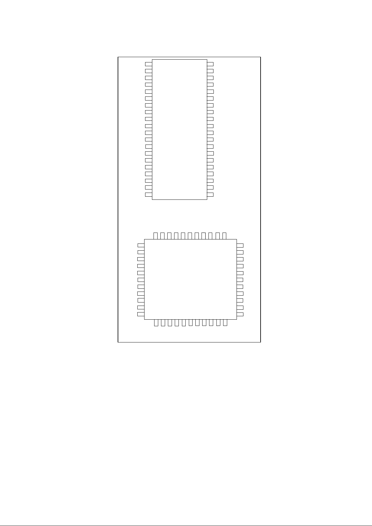
PIN CONFIGURATIONS
T0
X1
X2
nRESET
V
CC
CS
GND
nRD
A2
nWR
NC
D0
D1
D2
D3
D4
D5
D6
D7
GND
1
2
3
4
5
6
7
8
9
10
11
12
13
14
15
16
17
18
19
20
40
39
38
37
36
35
34
33
32
31
30
29
28
27
26
25
24
23
22
21
V
CC
T1
P27(KDAT)
P26(KCLK)
P25(IEMP/MINT)
P24(KINT)
P17(KINH)
P16(DISP)
P15(JUMP)
P14(RAM)
P13
P12
P11
P10
NC
V
CC
P23(NC/MCLK)
P22(NC/MDAT)
P21(nGA20)
P20(nRC)
40 Pin DIP
7
8
9
10
11
12
13
14
15
16
17
nCS
GND
nRD
A2
nWR
NC
NC
D0
D1
D2
D3
1819202122232425262728
D4D5D6
D7
GND
NC
P20
P21
P22
P23
V
CC
39
38
37
36
35
34
33
32
31
30
29
P24
P17
P16
P15
P14
NC
P13
P12
P11
P10
NC
65432
1
4443424140
VCCnRESETX2X1T0NC
VCCT1
P27
P26
P25
44 Pin PLCC

4
PIN DESCRIPTION
PIN NO. FUNCTION
(40 Pin
DIP)
(44 Pin
PLCC) I/O NAME AT MODE PS/2 MODE
1 2 I T0 K/B Clock Input K/B Clock Input
2 3 I X1 Crystal Clock I/P Crystal Clock I/P
3 4 I X2 Crystal Clock I/P Crystal Clock I/P
4 5 I nRESET Chip Reset Chip Reset
5 6 - VCC Optional +5V Power
Supply
Optional + 5V Power
Supply
6 7 I nCS Chip Select Chip Select
7 8 - GND Optional Ground
Power
Optional Ground
Power
8 9 I nRD I/O Read I/O Read
9 10 I A2 Connect to AddressA2Connect to Address
A2
10 11 I nWR I/O Write I/O Write
11,26 1,12,13,
23,29,34
- NC Reserved Reserved
12,13,14,
15,16,17,
18,19
14,15,16,
17,18,19,
20,21
I/O
D0−D7 Data Bus D0−D7 Data Bus D0−D7
20 22 - GND Ground Power
Supply
Ground Power Supply
21 24 O P20 Bit 0 of Port2
(nRC: System
Reset)
Bit 0 of Port2
(
nRC
: System Reset)
22 25 O P21 Bit 1 of Port2
(
nGA20
: GATE A20)
Bit 1 of Port2
(
nGA20
: GATE A20)
23 26 I/O P22 Bit 2 of Port2
(NC: User-defined
I/O)
Bit 2 of Port2
(MDAT: Mouse Data
Output)
24 27 I/O P23 Bit 3 of Port2
(NC: User-defined
I/O)
Bit 3 of Port2
(MCLK: Mouse Clock
Output)
25 28 - VCC Optional +5V Power
Supply
Optional + 5V Power
Supply
27 30 I/OPU* P10 Bit 0 of Port1
(User-defined I/O)
Bit 0 of Port1
(K/B Data Input)
28 31 I/OPU* P11 Bit 1 of Port1
(User-defined I/O)
Bit 1 of Port1
(Mouse Data Input)
29 32 I/O P12 Bit 2 of Port2
(User-defined I/O)
Bit 2 of Port2
(User-defined I/O)
30 33 I/O P13 Bit 3 of Port1
(User-defined I/O)
Bit 3 of Port1
(User-defined I/O)

5
PIN NO. FUNCTION
(40 Pin
DIP)
(44 Pin
PLCC) I/O NAME AT MODE PS/2 MODE
31 35 I PU* P14 Bit 4 of Port1
(RAM: RAM Jumper
Select)
Bit 4 of Port1
(RAM: RAM Jumper
Select)
32 36 I PU* P15 Bit 5 of Port1
(JUMP: Jumper)
Bit 5 of Port1
(JUMP: Jumper)
33 37 I PU* P16 Bit 6 of Port1
(DISP: Display
Select)
Bit 6 of Port1
(DISP: Display
Select)
34 38 I
PU*
P17 Bit 7 of Port1
(KINH: K/B Inhibit
Switch)
Bit 7 of Port1
(KINH: K/B Inhibit
Switch)
35 39 O P24 Bit 4 of Port2
(KINT: K/B OBF O/P
Interrupt)
Bit 4 of Port2
(KINT: K/B OBF O/P
Interrupt)
36 40 O P25 Bit 5 of Port2
(IEMP: I/P Buffer
Empty)
Bit 5 of Port2
(MINT: Mouse OBF
O/P Interrupt)
37 41 O P26 Bit 6 of Port2
(KCLK: K/B Clock
Output)
Bit 6 of Port2
(KCLK: K/B Clock
Output)
38 42 O P27 Bit 7 of Port2
(KDAT: K/B Data
Output)
Bit 7 of Port2
(KDAT: K/B Data
Output)
39 43 I T1 K/B Data Input Mouse Clock Input
40 44 - Vcc +5V Power Supply +5V Power Supply
* Internal pull-up resistor
6
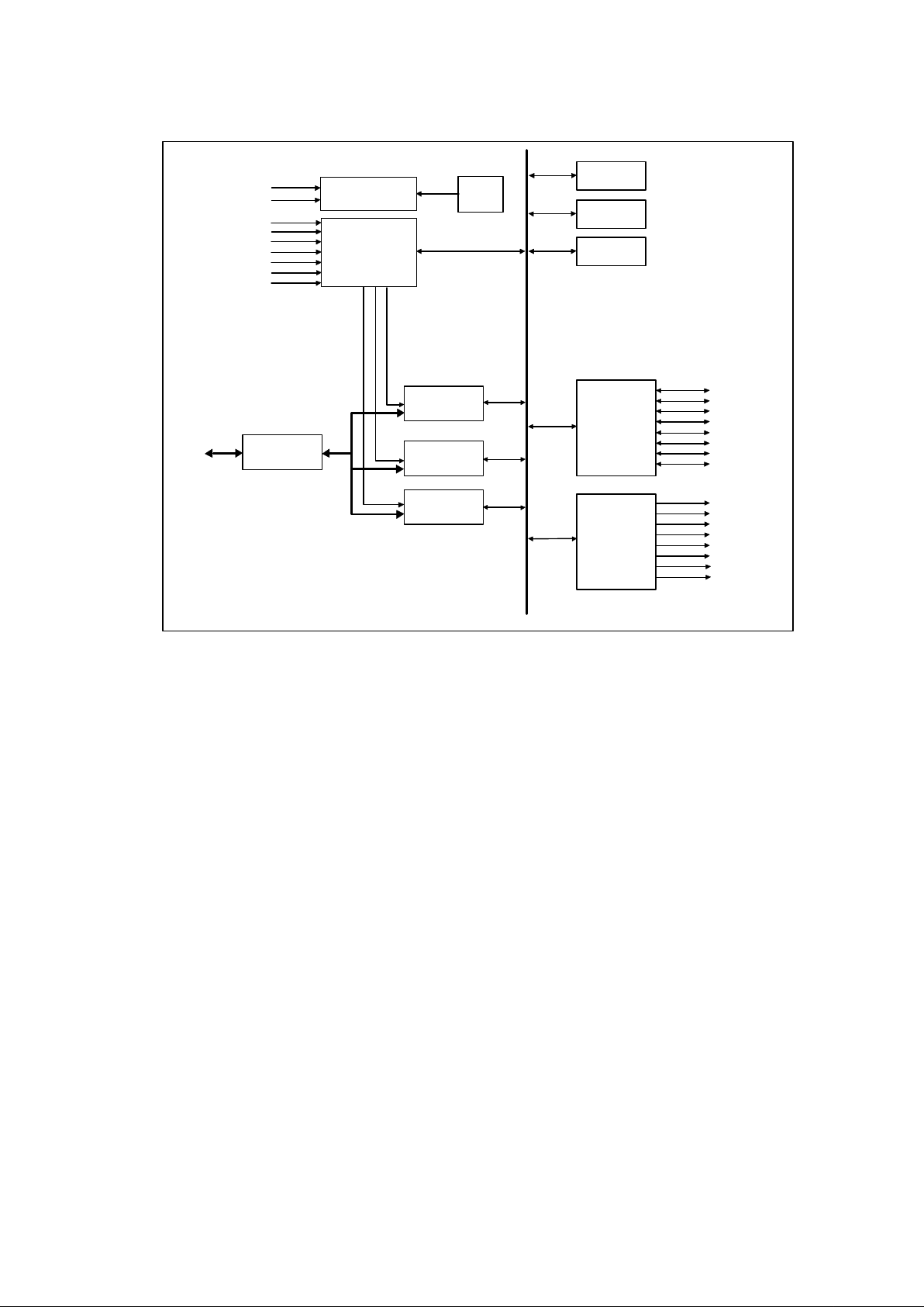
BLOCK DIAGRAM
SCAN
CODE
ROM
RECEIVE
CONTROL
HARDWIRE
CONTROL &
SELECT
LOGIC
STATUS
BUFFER
REGISTER
R64
W60
W64
R60
INPUT
BUFFER
REGISTER
BUFFER
REGISTER
OUTPUT
DATA
BUFFER
REGISTER
D0~D7
T0
T1
nWR
nRD
nCS
A2
nRESET
TRANSMIT
CONTRROL
REGISTER
STATUS
TRANSMIT
REGISTER
INPUT &
OUTPUT
PORT
INTERFACE
OUTPUT
PORT
INTERFACE
P20 (nRC)
P21 (nGA20)
P22 (NC/MDAT)
P23 (NC/MCLK)
P24 (KINT)
P25 (IEMP/MINT)
P26 (KCLK)
P27 (KDAT)
P10
P11
P12
P13
P14 (RAM)
P15 (JUMP)
P16 (DISP)
P17 (KINH)
x2
x1
7
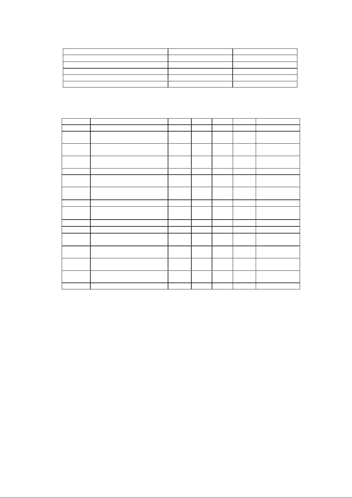
ABSOLUTE MAXIMUM RATINGS
PARAMETER RATING UNIT
Ambient Operating Temperature -0 to + 85
°C
Storage Temperature -65 to + 150
°C
Supply Voltage to Ground Potential -0.3 to + 7.0 V
Applied Input/Output Voltage -0.3 to + 7.0 V
Power Dissipation 50 mW
Note: Exposure to conditions beyond those listed under Absolute Maximum Ratings may adversely
affect the life and reliability of the device.
ELECTRICAL CHARACTERISTICS & CAPACITANCE
(Ta = 0° C to + 70° C, VDD = +5V ± 5%)
SYMBOL DESCRIPTION MIN. TYP. MAX. UNIT NOTE
VDD Power Supply 4.75 5.0 5.25 V
VIL Input Low Voltage (except
RESET, T0, T1)
0.8 V
VIL1 Input Low Voltage (RESET,
T0,T1)
0.6 V
VIH1 Input High Voltage (except
RESET, T0, T1, P10, P11)
2.0 V
VIH2 Input High Voltage (P10,P11) 3.0 V
VIH3 Input High Voltage (T0,T1,
RESET)
3.5 V
VOH1 Output High Voltage
(P10−P13, P20−P27)
2.4 V IOH = -2 mA
VOH2
Output High Voltage (D0−D7)
2.4 V IOH = -4 mA
VOL1
Output Low Voltage (P10−P13,
P20−P27)
0.4 V IOL = 2 mA
VOL2
Output Low Voltage (D0−D7)
0.4 V IOL = 4 mA
RIP Min. I/P Resist 10K
Ω
IOFL
O/P Leakage Current (D0−D7,
High Z State)
-10 10
µA
IIH I/P Leakage Current -10 10
µA
VDD = 5.5V,
VIN = VDD
IIL I/P Leakage Current (Except
P10, P11, P14, P15, P16, P17)
-10 10
µA
VDD = 5.5V,
VIN = VSS
IIL1 I/P Leakage Current (P10,
P11, P14, P15, P16, P17)
-10 550
µA
VDD = 5.5V,
VIN = VSS
CL O/P Load Capacity 15 50 pF
 Loading...