

SMSC KBD42W11 Datasheet

Keyboard Controller
FEATURES
KBD42W11
• Supports IBM PC and Compatible System
Designs
• Runs Much Faster Than Traditional
Keyboard Controllers
• Host interface Compatible with Traditional
Keyboard Controller
GENERAL DESCRIPTION
The KBD42W11 keyboard controller is
programmed to support the IBM® compatible
personal computer keyboard serial interface. The
keyboard controller receives serial data from the
keyboard, checks the parity of the data,
translates the scan code, and presents the data
to the system as a byte of data in its output
buffer. The controller will interrupt the system
when data is placed in its output buffer. The byte
of data will be sent to the keyboard serially with
an odd parity bit automatically inserted. The
keyboard is required to acknowledge all data
transmissions. No transmission should be sent to
the keyboard until acknowledgment is received
for the previous byte sent.
The KBD42W11 keyboard controller and BIOS to
improve the performance of IBM PC machines
and their compatibles. A hardwire methodology
• 6 MHz – 12 MHz Operating Frequency
• Communicates with Keyboard Directly
• High-reliability CMOS Technology
• 40 Pin DIP and 44 Pin PLCC Package
is used in this keyboard controller instead of a
software implementation, as in the traditional
8042 keyboard BIOS. This enables the keyboard
controller to respond instantly to all commands
sent from the keyboard to the CPU BIOS.
The KBD42W11 enables popular programs such
as AutoCAD®, Microsoft® Windows™, NOVELL®,
and other programs to run much faster.
IBM is a registered trademark of International Business
Machines Corporation. AutoCAD is a registered trademark
of Autodesk, Inc. Microsoft is a registered trademark and
Windows is a trademark of Microsoft Corporation.
NOVELL is a registered trademark of Novell, Inc.
Standard Microsystems is a registered trademark and
SMSC is a trademark of Standard Microsystems
Corporation. Other product and company names are
trademarks or registered trademarks of their respective
holders.

TABLE OF CONTENTS
FEATURES....................................................................................................................................... 1
GENERAL DESCRIPTION ................................................................................................................ 1
PIN CONFIGURATION...................................................................................................................... 3
PIN DESCRIPTION ........................................................................................................................... 4
BLOCK DIAGRAM............................................................................................................................ 5
AC TIMING........................................................................................................................................ 6
TIMING WAVEFORMS...................................................................................................................... 7
WRITE CYCLE TIMING ........................................................................................................................ 7
READ CYCLE TIMING.......................................................................................................................... 7
SEND DATA TO K/B...........................................................................................................................8
RECEIVE DATA FROM K/B................................................................................................................... 8
XIN/XOUT CLOCK ........................................................................................................................... 8
ABSOLUTE MAXIMUM RATINGS..................................................................................................... 9
ELECTRICAL CHARACTERISTICS & CAPACITANCE..................................................................... 9
STATUS REGISTER ....................................................................................................................... 10
OUTPUT BUFFER........................................................................................................................... 10
INPUT BUFFER .............................................................................................................................. 10
I/O PORTS...................................................................................................................................... 10
COMMANDS (I/O ADDRESS HEX 64)............................................................................................. 12
APPLICATION CIRCUIT ................................................................................................................. 13
ASYNCHRONOUS............................................................................................................................. 13
SYNCHRONOUS............................................................................................................................... 14
PACKAGE DIMENSIONS ................................................................................................................ 15
80 Arkay Drive
Hauppauge, NY 11788
(516) 435-6000
FAX (516) 273-3123
2
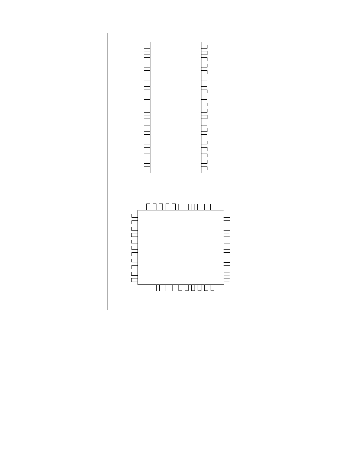
PIN CONFIGURATION
65432
1
4443424140
1819202122232425262728
D4D5D6
D7
VSS
NC
P20
P21
P22
P23
V
DD
VDDnRESET
XOUT
XINT0NC
VDDT1
P27
P28
P25
T0
X
X
OUT
nRESET
DD
V
nCS
SS
V
nRD
A2
nWR
NC
D0
D1
D2
D3
D4
D5
D6
D7
SS
V
40
V
1
IN
2
3
4
5
6
7
8
9
10
40 Pin DIP
11
12
13
14
15
16
17
18
19
20
39
38
37
36
35
34
33
32
31
30
29
28
27
26
25
24
23
22
21
DD
T1
P27(KDAT)
P26(KCLK)
P25(IEMP)
P24(INIT)
P17(KINH)
P16(DISP)
P15(JUMP)
P14(RAM)
P13
P12
P11
P10
NC
DD
V
P23
P22
P21(nGA20)
P20(nRC)
nCS
SS
V
nRD
A2
nWR
NC
NC
D0
D1
D2
D3
10
11
12
13
14
15
16
17
7
8
9
44 Pin PLCC
39
38
37
36
35
34
33
32
31
30
29
P24
P17
P18
P15
P14
NC
P13
P12
P11
P10
NC
3
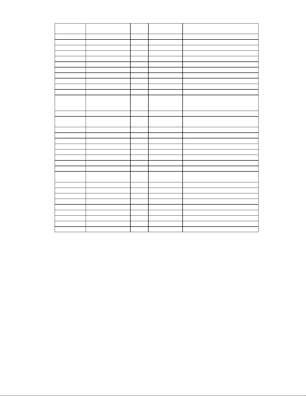
PIN DESCRIPTION
PIN NO.
(40 Pin DIP)
PIN NO.
(44 Pin PLCC) I/O NAME FUNCTION
1 2 I T0 K/B Clock Input
2 3 I XIN Crystal Clock I/P
3 4 O XOUT Crystal Clock O/P
4 5 I nRESET Chip Reset
5 6 - VDD Optional +5V Power Supply
6 7 I nCS Chip Select
7 8 - VSS Optional Ground Power
8 9 I nRD I/O Read
9 10 I A2 Connect to Address A2
10 11 I nWR I/O Write
11,26 1,12,13,23,29, 34 - NC Reserved
12,13,14,
15,16,17,
14,15,16,17,18,
19,20,21
I/O D0-D7 Data Bus D0 - D7
18, 19
20 22 - VSS Ground Power Supply
21 24 O P20 Bit 0 of Port 2 (RCB: System
Reset)
22 25 O P21 Bit 1 of Port 2 (GA20: GATE A20)
23 26 I/O P22 Bit 2 of Port 2
24 27 I/O P23 Bit 3 of Port 2
25 28 - VDD Optional +5V Power Supply
27 30 I/O P10 Bit 0 of Port 1
28 31 I/O P11 Bit 1 of Port 1
29 32 I/O P12 Bit 2 of Port 1
30 33 I/O P13 Bit 3 of Port 1
31 35 I P14 Bit 4 of Port 1 (RAM Jumper
Select)
32 36 I P15 Bit 5 of Port 1 (JUMP)
33 37 I P16 Bit 6 of Port 1 (Display Select)
34 38 I P17 Bit 7 of Port 1 (K/B Inhibit Switch)
35 39 O P24 Bit 4 of Port 2 (OBF O/P Interrupt)
36 40 O P25 Bit 5 of Port 2 (I/P Buffer Empty)
37 41 O P26 Bit 6 of Port 2 (K/B Clock O/P)
38 42 O P27 Bit 7 of Port 2 (K/B Data O/P)
39 43 I T1 K/B Data Input
40 44 - VDD +5V Power Supply
4
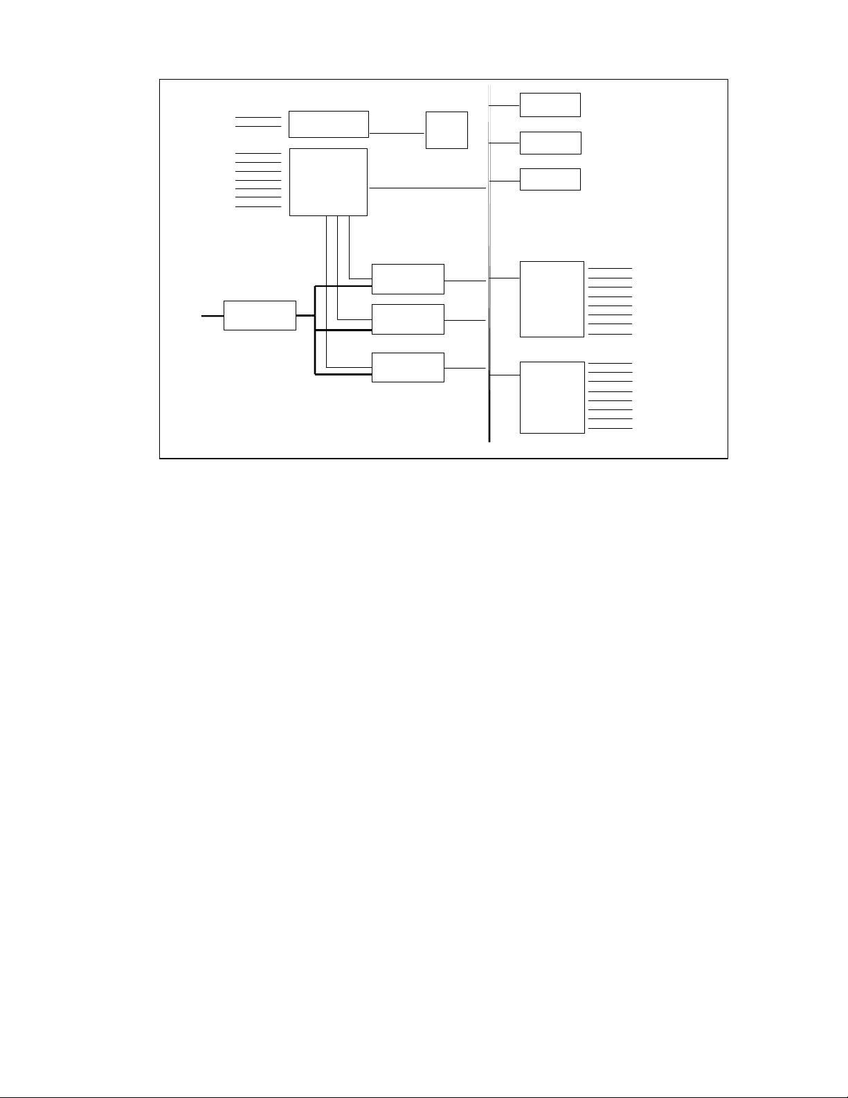
BLOCK DIAGRAM
T0
T1
XOUT
XIN
nWR
nRD
nCS
A2
nRESET
RECEIVE
CONTROL
HARDWIRE
CONTROL &
SELECT
LOGIC
SCAN
CODE
ROM
TRANSMIT
CONTROL
TRANSMIT
REGISTER
STATUS
REGISTER
D0- D7
DATA
BUFFER
REGISTER
R60
W60
W64
R64
STATUS
BUFFER
REGISTER
INPUT
BUFFER
REGISTER
OUTPUT
BUFFER
REGISTER
INPUT &
OUTPUT
PORT
INTERFACE
OUTPUT
PORT
INTERFACE
P10
P11
P12
P13
P14 (RAM Select)
P15 (Manufacture Mode)
P16 (Display)
P17 (KBNH)
(nRC)
P20
P21 (Gate A20)
P22
P23
P24
P25
P26 (Keyboard Clock)
(Keyboard Data)
P27
5
 Loading...