

SMSC EMC2305-1 Schematic [ru]
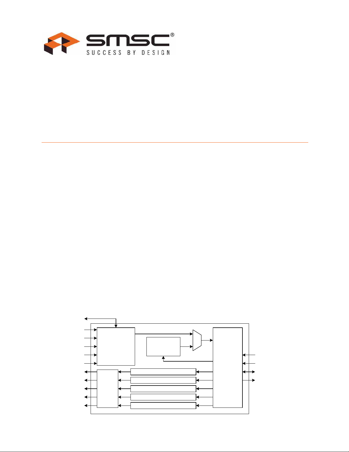
EMC2305
SMBus
Slave
Protocol
PWM
Drivers
SMCLK
SMDATA
Tachometer
Limit
Registers
PWM1
Tach
Measurement
TACH1
CLK
ADDR_SEL
ALERT#
PWM3
Fan Speed Control Algorithm
Fan Speed Control Algorithm
Fan Speed Control Algorithm
Fan Speed Control Algorithm
Fan Speed Control Algorithm
TACH2
TACH3
TACH4
PWM2
PWM4
PWM5
TACH5
Multiple RPM-Based PWM Fan Controller
for Five Fans
PRODUCT FEATURES
General Description
The EMC2305 is an SMBus compliant fan controller with
up to five independently controlled PWM fan drivers.
Each fan driver is controlled by a programmable
frequency PWM driver and Fan Speed Control algorithm
that operates in either a closed loop fashion or as a
directly PWM-controlled device.
The closed loop Fan Speed Control algorithm (FSC) has
the capability to detect aging fans and alert the system.
It will likewise detect stalled or locked fans and trigger
an interrupt.
Additionally, the EMC2305 offers a clock output so that
multiple devices may be chained and slaved to the
same clock source for optimal performance in large
distributed systems.
Applications
Servers
Projectors
Industrial and Networking Equipment
Notebook Computers
Datasheet
Features
Five Programmable Fan Control circuits (EMC2305)
— 4-wire fan compatible
— High speed PWM (26 kHz)
— Low speed PWM (9.5Hz - 2240 Hz)
— Optional detection of aging fans
— Fan Spin Up Control and Ramp Rate Control
— Alert on Fan Stall
— Up to 3 Selectable Default Fan Speeds
Watchdog Timer
RPM-based fan control algorithm
— 0.5% accuracy from 500 RPM to 16k RPM (external
crystal oscillator)
— 1% accuracy from 500 RPM to 16k RPM (internal clock)
SMBus 2.0 Compliant
— Up to 6 selectable SMBus addresses
— SMBus Alert compatible
CLK Pin can provide a clock source output
Available in a 16-pin 4mm x 4mm QFN Lead-free
RoHS Compliant package
Block Diagram
SMSC EMC2305 DATASHEET Revision 1.3 (05-18-11)
Multiple RPM-Based PWM Fan Controller for Five Fans
Order Number:
ORDERING NUMBER PACKAGE FEATURES
Datasheet
EMC2305-1-AP-TR 16-pin QFN (Lead-free
RoHS compliant)
Five RPM-based fan speed control
algorithms
This product meets the halogen maximum concentration values per IEC 61249-2-21
For RoHS compliance and environmental information, please visit
www.smsc.com/rohs
80 ARKAY DRIVE, HAUPPAUGE, NY 11788 (631) 435-6000 or 1 (800) 443-SEMI
Copyright © 2011 SMSC or its subsidiaries. All rights reserved.
Circuit diagrams and other information relating to SMSC products are included as a mean s of illustrating typical applications. Conse quently, complete information sufficient for
construction purposes is not necessarily given. Although the information has been checked and is believed to be accurate, no responsibility is assumed for inaccuracies. SMSC
reserves the right to make changes to specifications and product descriptions at any time without notice. Contact your local SMSC sales office to obtain the latest specifications
before placing your product order. The provision of this information does not convey to the purchaser of the described semiconductor devices any licenses under any patent
rights or other intellectual property rights of SMSC or others. All sales are expressly conditional on your agreement to the terms and conditions of the most recently da ted
version of SMSC's standard Terms of Sale Agreement dated before the date of your order (the "Terms of Sale Agreement"). The product may contain design defects or errors
known as anomalies which may cause the product's functions to deviate from published specifications. Anomaly sheets are available upon request. SMSC products are not
designed, intended, authorized or warranted for use in any life support or other application where product failure could cause or contribute to personal injury or severe property
damage. Any and all such uses without prior written approval of an Officer of SMSC and further testing and/or modification will be fully at the risk of the customer. Copies of
this document or other SMSC literature, as well as the Terms of Sale Agreement, may be obtained by visiting SMSC’s website at http://www.smsc.com. SMSC is a registered
trademark of Standard Microsystems Corporation (“SMSC”). Product names and company names are the trademarks of their respective holders.
SMSC DISCLAIMS AND EXCLUDES ANY AND ALL WARRANTIES, INCLUDING WITHOUT LIMITATION ANY AND ALL IMPLIED WARRANTIES OF MERCHANTABILITY,
FITNESS FOR A PARTICULAR PURPOSE, TITLE, AND AGAINST INFRINGEMENT AND THE LIKE, AND ANY AND ALL WARRANTIES ARISING FROM ANY COURSE
OF DEALING OR USAGE OF TRADE. IN NO EVENT SHALL SMSC BE LIABLE FOR ANY DIRECT, INCIDENTAL, INDIRECT, SPECIAL, PUNITIVE, OR CONSEQUENTIAL
DAMAGES; OR FOR LOST DATA, PROFITS, SAVINGS OR REVENUES OF ANY KIND; REGARDLESS OF THE FORM OF ACTION, WHETHER BASED ON CONTRACT;
TORT; NEGLIGENCE OF SMSC OR OTHERS; STRICT LIABILITY; BREACH OF WARRANTY; OR OTHERWISE; WHETHER OR NOT ANY REMEDY OF BUYER IS HELD
TO HAVE FAILED OF ITS ESSENTIAL PURPOSE, AND WHETHER OR NOT SMSC HAS BEEN ADVISED OF THE POSSIBILITY OF SUCH DAMAGES.
Revision 1.3 (05-18-11) 2 SMSC EMC2305
DATASHEET
Multiple RPM-Based PWM Fan Controller for Five Fans
Datasheet
Table of Contents
Chapter 1 Pin Description. . . . . . . . . . . . . . . . . . . . . . . . . . . . . . . . . . . . . . . . . . . . . . . . . . . . . 7
Chapter 2 Electrical Specifications . . . . . . . . . . . . . . . . . . . . . . . . . . . . . . . . . . . . . . . . . . . . 10
2.1 Electrical Specifications . . . . . . . . . . . . . . . . . . . . . . . . . . . . . . . . . . . . . . . . . . . . . . . . . . . . . . . . . 10
2.2 SMBus Electrical Specifications . . . . . . . . . . . . . . . . . . . . . . . . . . . . . . . . . . . . . . . . . . . . . . . . . . . 11
Chapter 3 Communications . . . . . . . . . . . . . . . . . . . . . . . . . . . . . . . . . . . . . . . . . . . . . . . . . . 13
3.1 System Management Bus Interface Protocol . . . . . . . . . . . . . . . . . . . . . . . . . . . . . . . . . . . . . . . . . 13
3.1.1 SMBus Start Bit . . . . . . . . . . . . . . . . . . . . . . . . . . . . . . . . . . . . . . . . . . . . . . . . . . . . . . . . 13
3.1.2 SMBus Address and RD / WR
3.1.3 SMBus Data Bytes . . . . . . . . . . . . . . . . . . . . . . . . . . . . . . . . . . . . . . . . . . . . . . . . . . . . . 14
3.1.4 SMBus ACK and NACK Bits . . . . . . . . . . . . . . . . . . . . . . . . . . . . . . . . . . . . . . . . . . . . . . 14
3.1.5 SMBus Stop Bit . . . . . . . . . . . . . . . . . . . . . . . . . . . . . . . . . . . . . . . . . . . . . . . . . . . . . . . . 14
3.1.6 SMBus Time-out . . . . . . . . . . . . . . . . . . . . . . . . . . . . . . . . . . . . . . . . . . . . . . . . . . . . . . . 14
3.1.7 SMBus and I
3.2 SMBus Protocols . . . . . . . . . . . . . . . . . . . . . . . . . . . . . . . . . . . . . . . . . . . . . . . . . . . . . . . . . . . . . . 15
3.2.1 Write Byte . . . . . . . . . . . . . . . . . . . . . . . . . . . . . . . . . . . . . . . . . . . . . . . . . . . . . . . . . . . . 15
3.2.2 Read Byte . . . . . . . . . . . . . . . . . . . . . . . . . . . . . . . . . . . . . . . . . . . . . . . . . . . . . . . . . . . . 15
3.2.3 Send Byte . . . . . . . . . . . . . . . . . . . . . . . . . . . . . . . . . . . . . . . . . . . . . . . . . . . . . . . . . . . . 15
3.2.4 Receive Byte . . . . . . . . . . . . . . . . . . . . . . . . . . . . . . . . . . . . . . . . . . . . . . . . . . . . . . . . . . 16
3.2.5 Block Write Protocol . . . . . . . . . . . . . . . . . . . . . . . . . . . . . . . . . . . . . . . . . . . . . . . . . . . . 16
3.2.6 Block Read Protocol . . . . . . . . . . . . . . . . . . . . . . . . . . . . . . . . . . . . . . . . . . . . . . . . . . . . 16
3.2.7 Alert Response Address . . . . . . . . . . . . . . . . . . . . . . . . . . . . . . . . . . . . . . . . . . . . . . . . . 16
2
C Compliance . . . . . . . . . . . . . . . . . . . . . . . . . . . . . . . . . . . . . . . . . . . . . . 14
Bit . . . . . . . . . . . . . . . . . . . . . . . . . . . . . . . . . . . . . . . . . . 13
Chapter 4 Product Description. . . . . . . . . . . . . . . . . . . . . . . . . . . . . . . . . . . . . . . . . . . . . . . . 18
4.1 Fan Control Modes of Operation . . . . . . . . . . . . . . . . . . . . . . . . . . . . . . . . . . . . . . . . . . . . . . . . . . 18
4.2 PWM Fan Driver . . . . . . . . . . . . . . . . . . . . . . . . . . . . . . . . . . . . . . . . . . . . . . . . . . . . . . . . . . . . . . . 19
4.3 RPM-based Fan Speed Control Algorithm (FSC). . . . . . . . . . . . . . . . . . . . . . . . . . . . . . . . . . . . . . 19
4.3.1 Programming the RPM-based Fan Speed Control Algorithm . . . . . . . . . . . . . . . . . . . . . 20
4.4 Tachometer Measurement . . . . . . . . . . . . . . . . . . . . . . . . . . . . . . . . . . . . . . . . . . . . . . . . . . . . . . . 20
4.4.1 Stalled Fan . . . . . . . . . . . . . . . . . . . . . . . . . . . . . . . . . . . . . . . . . . . . . . . . . . . . . . . . . . . 21
4.4.2 Aging Fan or Invalid Drive Detection. . . . . . . . . . . . . . . . . . . . . . . . . . . . . . . . . . . . . . . . 21
4.5 CLK Pin. . . . . . . . . . . . . . . . . . . . . . . . . . . . . . . . . . . . . . . . . . . . . . . . . . . . . . . . . . . . . . . . . . . . . . 21
4.5.1 Pull Up Decode . . . . . . . . . . . . . . . . . . . . . . . . . . . . . . . . . . . . . . . . . . . . . . . . . . . . . . . . 21
4.5.2 External Clock . . . . . . . . . . . . . . . . . . . . . . . . . . . . . . . . . . . . . . . . . . . . . . . . . . . . . . . . . 22
4.5.3 Internal Clock. . . . . . . . . . . . . . . . . . . . . . . . . . . . . . . . . . . . . . . . . . . . . . . . . . . . . . . . . . 22
4.6 Spin Up Routine . . . . . . . . . . . . . . . . . . . . . . . . . . . . . . . . . . . . . . . . . . . . . . . . . . . . . . . . . . . . . . . 22
4.6.1 Power Up Options . . . . . . . . . . . . . . . . . . . . . . . . . . . . . . . . . . . . . . . . . . . . . . . . . . . . . . 23
4.7 Ramp Rate Control. . . . . . . . . . . . . . . . . . . . . . . . . . . . . . . . . . . . . . . . . . . . . . . . . . . . . . . . . . . . . 23
4.8 Watchdog Timer . . . . . . . . . . . . . . . . . . . . . . . . . . . . . . . . . . . . . . . . . . . . . . . . . . . . . . . . . . . . . . . 24
4.8.1 Power Up Operation . . . . . . . . . . . . . . . . . . . . . . . . . . . . . . . . . . . . . . . . . . . . . . . . . . . . 24
4.8.2 Continuous Operation . . . . . . . . . . . . . . . . . . . . . . . . . . . . . . . . . . . . . . . . . . . . . . . . . . . 25
Chapter 5 Register Set. . . . . . . . . . . . . . . . . . . . . . . . . . . . . . . . . . . . . . . . . . . . . . . . . . . . . . . 26
5.1 Register Map . . . . . . . . . . . . . . . . . . . . . . . . . . . . . . . . . . . . . . . . . . . . . . . . . . . . . . . . . . . . . . . . . 26
5.1.1 Lock Entries. . . . . . . . . . . . . . . . . . . . . . . . . . . . . . . . . . . . . . . . . . . . . . . . . . . . . . . . . . . 31
5.2 Configuration Register . . . . . . . . . . . . . . . . . . . . . . . . . . . . . . . . . . . . . . . . . . . . . . . . . . . . . . . . . . 31
5.3 Fan Status Registers . . . . . . . . . . . . . . . . . . . . . . . . . . . . . . . . . . . . . . . . . . . . . . . . . . . . . . . . . . . 32
5.3.1 Fan Status - 24h . . . . . . . . . . . . . . . . . . . . . . . . . . . . . . . . . . . . . . . . . . . . . . . . . . . . . . . 32
5.3.2 Fan Stall Status - 25h . . . . . . . . . . . . . . . . . . . . . . . . . . . . . . . . . . . . . . . . . . . . . . . . . . . 33
SMSC EMC2305 3 Revision 1.3 (05-18-11)
DATASHEET

Multiple RPM-Based PWM Fan Controller for Five Fans
Datasheet
5.3.3 Fan Spin Status - 26h . . . . . . . . . . . . . . . . . . . . . . . . . . . . . . . . . . . . . . . . . . . . . . . . . . . 33
5.3.4 Fan Drive Fail Status - 27h . . . . . . . . . . . . . . . . . . . . . . . . . . . . . . . . . . . . . . . . . . . . . . . 33
5.4 Fan Interrupt Enable Register. . . . . . . . . . . . . . . . . . . . . . . . . . . . . . . . . . . . . . . . . . . . . . . . . . . . . 33
5.5 PWM Configuration Registers . . . . . . . . . . . . . . . . . . . . . . . . . . . . . . . . . . . . . . . . . . . . . . . . . . . . 34
5.5.1 PWM Polarity Config - 2Ah . . . . . . . . . . . . . . . . . . . . . . . . . . . . . . . . . . . . . . . . . . . . . . . 34
5.5.2 PWM Output Config - 2Bh. . . . . . . . . . . . . . . . . . . . . . . . . . . . . . . . . . . . . . . . . . . . . . . . 34
5.6 PWM Base Frequency Registers . . . . . . . . . . . . . . . . . . . . . . . . . . . . . . . . . . . . . . . . . . . . . . . . . . 35
5.6.1 PWM Base Frequency 1 - 2Bh . . . . . . . . . . . . . . . . . . . . . . . . . . . . . . . . . . . . . . . . . . . . 35
5.6.2 PWM Base Frequency 2 - 2Ch . . . . . . . . . . . . . . . . . . . . . . . . . . . . . . . . . . . . . . . . . . . . 35
5.7 Fan Setting Registers. . . . . . . . . . . . . . . . . . . . . . . . . . . . . . . . . . . . . . . . . . . . . . . . . . . . . . . . . . . 36
5.8 PWM Divide Registers . . . . . . . . . . . . . . . . . . . . . . . . . . . . . . . . . . . . . . . . . . . . . . . . . . . . . . . . . . 36
5.9 Fan Configuration 1 Registers . . . . . . . . . . . . . . . . . . . . . . . . . . . . . . . . . . . . . . . . . . . . . . . . . . . . 37
5.10 Fan Configuration 2 Registers . . . . . . . . . . . . . . . . . . . . . . . . . . . . . . . . . . . . . . . . . . . . . . . . . . . . 38
5.11 Gain Registers . . . . . . . . . . . . . . . . . . . . . . . . . . . . . . . . . . . . . . . . . . . . . . . . . . . . . . . . . . . . . . . . 40
5.12 Fan Spin Up Configuration Registers . . . . . . . . . . . . . . . . . . . . . . . . . . . . . . . . . . . . . . . . . . . . . . . 41
5.13 Fan Max Step Registers. . . . . . . . . . . . . . . . . . . . . . . . . . . . . . . . . . . . . . . . . . . . . . . . . . . . . . . . . 43
5.14 Fan Minimum Drive Registers . . . . . . . . . . . . . . . . . . . . . . . . . . . . . . . . . . . . . . . . . . . . . . . . . . . . 44
5.15 Valid TACH Count Registers . . . . . . . . . . . . . . . . . . . . . . . . . . . . . . . . . . . . . . . . . . . . . . . . . . . . . 44
5.16 Fan Drive Fail Band Registers . . . . . . . . . . . . . . . . . . . . . . . . . . . . . . . . . . . . . . . . . . . . . . . . . . . . 45
5.17 TACH Target Registers . . . . . . . . . . . . . . . . . . . . . . . . . . . . . . . . . . . . . . . . . . . . . . . . . . . . . . . . . 46
5.18 TACH Reading Registers . . . . . . . . . . . . . . . . . . . . . . . . . . . . . . . . . . . . . . . . . . . . . . . . . . . . . . . . 47
5.19 Software Lock Register. . . . . . . . . . . . . . . . . . . . . . . . . . . . . . . . . . . . . . . . . . . . . . . . . . . . . . . . . . 48
5.20 Product Features Register . . . . . . . . . . . . . . . . . . . . . . . . . . . . . . . . . . . . . . . . . . . . . . . . . . . . . . . 48
5.21 Product ID Register . . . . . . . . . . . . . . . . . . . . . . . . . . . . . . . . . . . . . . . . . . . . . . . . . . . . . . . . . . . . 49
5.22 Manufacturer ID Register . . . . . . . . . . . . . . . . . . . . . . . . . . . . . . . . . . . . . . . . . . . . . . . . . . . . . . . . 50
5.23 Revision Register . . . . . . . . . . . . . . . . . . . . . . . . . . . . . . . . . . . . . . . . . . . . . . . . . . . . . . . . . . . . . . 50
Chapter 6 Typical Operating Curves. . . . . . . . . . . . . . . . . . . . . . . . . . . . . . . . . . . . . . . . . . . 51
Chapter 7 Package Drawing . . . . . . . . . . . . . . . . . . . . . . . . . . . . . . . . . . . . . . . . . . . . . . . . . . 53
7.1 EMC2305 Package Information . . . . . . . . . . . . . . . . . . . . . . . . . . . . . . . . . . . . . . . . . . . . . . . . . . . 53
7.2 Package Markings . . . . . . . . . . . . . . . . . . . . . . . . . . . . . . . . . . . . . . . . . . . . . . . . . . . . . . . . . . . . . 55
Chapter 8 Datasheet Revision History. . . . . . . . . . . . . . . . . . . . . . . . . . . . . . . . . . . . . . . . . . 56
Revision 1.3 (05-18-11) 4 SMSC EMC2305
DATASHEET

Multiple RPM-Based PWM Fan Controller for Five Fans
Datasheet
List of Figures
Figure 1.1 EMC2305 Pin Diagram (16-Pin QFN) . . . . . . . . . . . . . . . . . . . . . . . . . . . . . . . . . . . . . . . . . . . 7
Figure 3.1 SMBus Timing Diagram. . . . . . . . . . . . . . . . . . . . . . . . . . . . . . . . . . . . . . . . . . . . . . . . . . . . . 13
Figure 4.1 System Diagram of EMC2305 . . . . . . . . . . . . . . . . . . . . . . . . . . . . . . . . . . . . . . . . . . . . . . . . 18
Figure 4.2 Spin Up Routine. . . . . . . . . . . . . . . . . . . . . . . . . . . . . . . . . . . . . . . . . . . . . . . . . . . . . . . . . . . 23
Figure 4.3 Ramp Rate Control . . . . . . . . . . . . . . . . . . . . . . . . . . . . . . . . . . . . . . . . . . . . . . . . . . . . . . . . 24
Figure 7.1 Package Drawing - 16-Pin QFN 4mm x 4mm . . . . . . . . . . . . . . . . . . . . . . . . . . . . . . . . . . . . 53
Figure 7.2 Package Dimensions - 16-Pin QFN 4mm x 4mm . . . . . . . . . . . . . . . . . . . . . . . . . . . . . . . . . 54
Figure 7.3 PCB Footprint - 16-Pin QFN 4mm x 4mm . . . . . . . . . . . . . . . . . . . . . . . . . . . . . . . . . . . . . . . 54
Figure 7.4 EMC2305 Package Markings. . . . . . . . . . . . . . . . . . . . . . . . . . . . . . . . . . . . . . . . . . . . . . . . . 55
SMSC EMC2305 5 Revision 1.3 (05-18-11)
DATASHEET

Multiple RPM-Based PWM Fan Controller for Five Fans
Datasheet
List of Tables
Table 1.1 Pin Description for EMC2305 . . . . . . . . . . . . . . . . . . . . . . . . . . . . . . . . . . . . . . . . . . . . . . . . . . 7
Table 1.2 Pin Types. . . . . . . . . . . . . . . . . . . . . . . . . . . . . . . . . . . . . . . . . . . . . . . . . . . . . . . . . . . . . . . . . . 9
Table 2.1 Absolute Maximum Ratings. . . . . . . . . . . . . . . . . . . . . . . . . . . . . . . . . . . . . . . . . . . . . . . . . . . 10
Table 2.2 Electrical Specifications. . . . . . . . . . . . . . . . . . . . . . . . . . . . . . . . . . . . . . . . . . . . . . . . . . . . . . 10
Table 2.3 SMBus Electrical Specifications . . . . . . . . . . . . . . . . . . . . . . . . . . . . . . . . . . . . . . . . . . . . . . . 11
Table 3.1 ADDR_SEL Pin Decode . . . . . . . . . . . . . . . . . . . . . . . . . . . . . . . . . . . . . . . . . . . . . . . . . . . . . 14
Table 3.2 Protocol Format . . . . . . . . . . . . . . . . . . . . . . . . . . . . . . . . . . . . . . . . . . . . . . . . . . . . . . . . . . . . 15
Table 3.3 Write Byte Protocol . . . . . . . . . . . . . . . . . . . . . . . . . . . . . . . . . . . . . . . . . . . . . . . . . . . . . . . . . 15
Table 3.4 Read Byte Protocol . . . . . . . . . . . . . . . . . . . . . . . . . . . . . . . . . . . . . . . . . . . . . . . . . . . . . . . . . 15
Table 3.5 Send Byte Protocol . . . . . . . . . . . . . . . . . . . . . . . . . . . . . . . . . . . . . . . . . . . . . . . . . . . . . . . . . 15
Table 3.6 Receive Byte Protocol . . . . . . . . . . . . . . . . . . . . . . . . . . . . . . . . . . . . . . . . . . . . . . . . . . . . . . . 16
Table 3.7 Block Write Protocol . . . . . . . . . . . . . . . . . . . . . . . . . . . . . . . . . . . . . . . . . . . . . . . . . . . . . . . . 16
Table 3.8 Block Read Protocol . . . . . . . . . . . . . . . . . . . . . . . . . . . . . . . . . . . . . . . . . . . . . . . . . . . . . . . . 16
Table 3.9 Alert Response Address Protocol . . . . . . . . . . . . . . . . . . . . . . . . . . . . . . . . . . . . . . . . . . . . . . 17
Table 4.1 Fan Controls Active for Operating Mode . . . . . . . . . . . . . . . . . . . . . . . . . . . . . . . . . . . . . . . . . 19
Table 4.2 CLK Pin Pull-Up Decode . . . . . . . . . . . . . . . . . . . . . . . . . . . . . . . . . . . . . . . . . . . . . . . . . . . . . 21
Table 5.1 EMC2305 Register Set . . . . . . . . . . . . . . . . . . . . . . . . . . . . . . . . . . . . . . . . . . . . . . . . . . . . . . 26
Table 5.2 Configuration Register. . . . . . . . . . . . . . . . . . . . . . . . . . . . . . . . . . . . . . . . . . . . . . . . . . . . . . . 31
Table 5.3 Fan Status Registers . . . . . . . . . . . . . . . . . . . . . . . . . . . . . . . . . . . . . . . . . . . . . . . . . . . . . . . . 32
Table 5.4 Fan Interrupt Enable Register . . . . . . . . . . . . . . . . . . . . . . . . . . . . . . . . . . . . . . . . . . . . . . . . . 33
Table 5.5 PWM Configuration Registers . . . . . . . . . . . . . . . . . . . . . . . . . . . . . . . . . . . . . . . . . . . . . . . . . 34
Table 5.6 PWM Base Frequency Registers. . . . . . . . . . . . . . . . . . . . . . . . . . . . . . . . . . . . . . . . . . . . . . . 35
Table 5.7 PWM_BASEx[1:0] Bit Decode. . . . . . . . . . . . . . . . . . . . . . . . . . . . . . . . . . . . . . . . . . . . . . . . . 35
Table 5.8 Fan Driver Setting Registers . . . . . . . . . . . . . . . . . . . . . . . . . . . . . . . . . . . . . . . . . . . . . . . . . . 36
Table 5.9 PWM Divide Registers. . . . . . . . . . . . . . . . . . . . . . . . . . . . . . . . . . . . . . . . . . . . . . . . . . . . . . . 36
Table 5.10 Fan Configuration 1 Registers. . . . . . . . . . . . . . . . . . . . . . . . . . . . . . . . . . . . . . . . . . . . . . . . . 37
Table 5.11 Range Decode. . . . . . . . . . . . . . . . . . . . . . . . . . . . . . . . . . . . . . . . . . . . . . . . . . . . . . . . . . . . . 37
Table 5.12 Minimum Edges for Fan Rotation . . . . . . . . . . . . . . . . . . . . . . . . . . . . . . . . . . . . . . . . . . . . . . 38
Table 5.13 Update Time . . . . . . . . . . . . . . . . . . . . . . . . . . . . . . . . . . . . . . . . . . . . . . . . . . . . . . . . . . . . . . 38
Table 5.14 Fan Configuration 2 Registers. . . . . . . . . . . . . . . . . . . . . . . . . . . . . . . . . . . . . . . . . . . . . . . . . 38
Table 5.15 Derivative Options . . . . . . . . . . . . . . . . . . . . . . . . . . . . . . . . . . . . . . . . . . . . . . . . . . . . . . . . . . 39
Table 5.16 Error Range Options . . . . . . . . . . . . . . . . . . . . . . . . . . . . . . . . . . . . . . . . . . . . . . . . . . . . . . . . 40
Table 5.17 Gain Registers. . . . . . . . . . . . . . . . . . . . . . . . . . . . . . . . . . . . . . . . . . . . . . . . . . . . . . . . . . . . . 40
Table 5.18 Gain Decode . . . . . . . . . . . . . . . . . . . . . . . . . . . . . . . . . . . . . . . . . . . . . . . . . . . . . . . . . . . . . . 41
Table 5.19 Fan Spin Up Configuration Registers . . . . . . . . . . . . . . . . . . . . . . . . . . . . . . . . . . . . . . . . . . . 41
Table 5.20 DRIVE_FAIL_CNT[1:0] Bit Decode . . . . . . . . . . . . . . . . . . . . . . . . . . . . . . . . . . . . . . . . . . . . . 41
Table 5.21 Spin Level . . . . . . . . . . . . . . . . . . . . . . . . . . . . . . . . . . . . . . . . . . . . . . . . . . . . . . . . . . . . . . . . 42
Table 5.22 Spin Time. . . . . . . . . . . . . . . . . . . . . . . . . . . . . . . . . . . . . . . . . . . . . . . . . . . . . . . . . . . . . . . . . 43
Table 5.23 Fan Max Step Registers . . . . . . . . . . . . . . . . . . . . . . . . . . . . . . . . . . . . . . . . . . . . . . . . . . . . . 43
Table 5.24Minimum Fan Drive Registers . . . . . . . . . . . . . . . . . . . . . . . . . . . . . . . . . . . . . . . . . . . . . . . . . 44
Table 5.25 Valid TACH Count Registers. . . . . . . . . . . . . . . . . . . . . . . . . . . . . . . . . . . . . . . . . . . . . . . . . . 44
Table 5.26 Fan Drive Fail Band Registers. . . . . . . . . . . . . . . . . . . . . . . . . . . . . . . . . . . . . . . . . . . . . . . . . 45
Table 5.27 TACH Target Registers . . . . . . . . . . . . . . . . . . . . . . . . . . . . . . . . . . . . . . . . . . . . . . . . . . . . . . 46
Table 5.28 TACH Reading Registers . . . . . . . . . . . . . . . . . . . . . . . . . . . . . . . . . . . . . . . . . . . . . . . . . . . . 47
Table 5.29 Software Lock Register . . . . . . . . . . . . . . . . . . . . . . . . . . . . . . . . . . . . . . . . . . . . . . . . . . . . . . 48
Table 5.30 Product Features Register. . . . . . . . . . . . . . . . . . . . . . . . . . . . . . . . . . . . . . . . . . . . . . . . . . . . 48
Table 5.31 ADDR_SEL Pin Configuration. . . . . . . . . . . . . . . . . . . . . . . . . . . . . . . . . . . . . . . . . . . . . .
Table 5.32 FAN_SPD Pin Configuration . . . . . . . . . . . . . . . . . . . . . . . . . . . . . . . . . . . . . . . . . . . . . . . . . . 49
Table 5.33 Product ID Register . . . . . . . . . . . . . . . . . . . . . . . . . . . . . . . . . . . . . . . . . . . . . . . . . . . . . . . . . 49
Table 5.34 Manufacturer ID Register. . . . . . . . . . . . . . . . . . . . . . . . . . . . . . . . . . . . . . . . . . . . . . . . . . . . . 50
Table 5.35 Revision Register. . . . . . . . . . . . . . . . . . . . . . . . . . . . . . . . . . . . . . . . . . . . . . . . . . . . . . . . . . . 50
Table 8.1 Customer Revision History . . . . . . . . . . . . . . . . . . . . . . . . . . . . . . . . . . . . . . . . . . . . . . . . . . . 56
. . . 49
Revision 1.3 (05-18-11) 6 SMSC EMC2305
DATASHEET
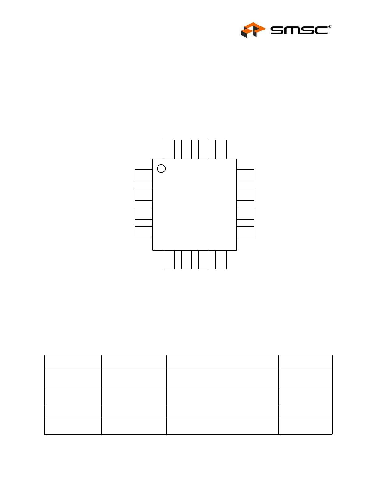
Multiple RPM-Based PWM Fan Controller for Five Fans
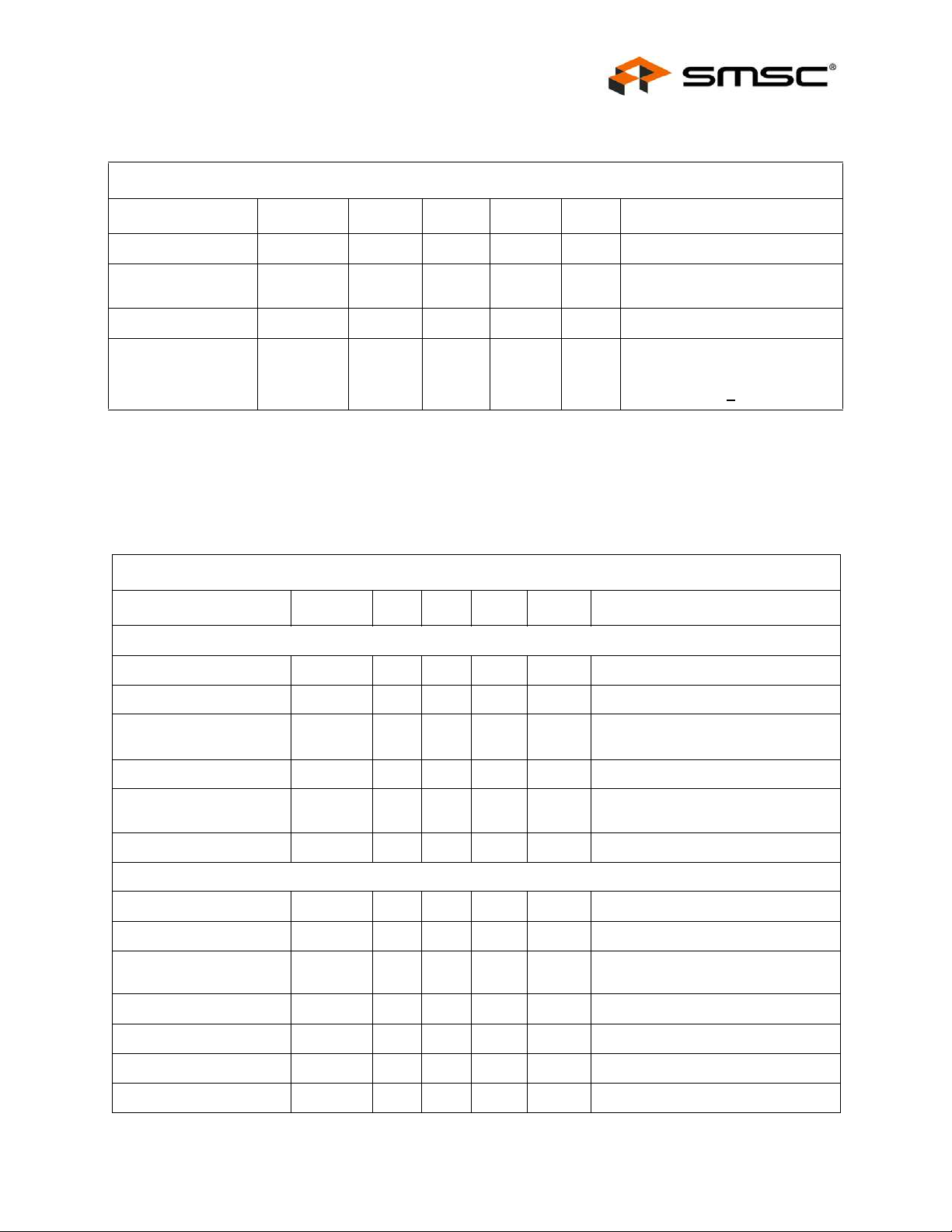
EMC2305
16-QFN
1
2
3
4
5
6
7
8
12
11
10
9
16
15
14
13
VDD
SMCLK
PWM1
TACH2
SMDATA
CLK
ADDR_SEL
TACH1
PWM2
PWM 3
TACH3
ALERT#
PWM4
TACH4
TACH5
PWM5
Datasheet
Chapter 1 Pin Description
PIN NUMBER PIN NAME PIN FUNCTION PIN TYPE
1SMDATA
2SMCLK
3 VDD Power Supply Power
4 ADDR_SEL
SMSC EMC2305 7 Revision 1.3 (05-18-11)
Figure 1.1 EMC2305 Pin Diag ram (16-Pin QFN)
Ta bl e 1.1 Pin Description for EMC2305
SMBus data input/output - requires
external pull-up resistor
SMBus clock input - requires external
pull-up resistor
Address selection input - requires pull-up
resistor
DATASHEET
DIOD (5V)
DI (5V)
AIO

Multiple RPM-Based PWM Fan Controller for Five Fans
Datasheet
Table 1.1 Pin Description for EMC2305 (continued)
PIN NUMBER PIN NAME PIN FUNCTION PIN TYPE
5PWM1
Push-Pull PWM output driver for Fan 1 DO
Open Drain PWM output driver for Fan 1 OD (5V)
6TACH1
Open drain tachometer input for Fan 1-
Push-Pull PWM output driver for Fan 2 DO
7PWM2
Open Drain PWM output driver for Fan 2 OD (5V)
8TACH2
Open drain tachometer input for Fan 2 -
Push-Pull PWM output driver for Fan 3 DO
9PWM3
Open Drain PWM output driver for Fan 3 OD (5V)
10 TACH3
Open drain tachometer input for Fan 3 -
Clock input for tachometer measurement DI (5V)
11 CLK
Push Pull Clock output to other fan
controllers to synchronize Fan Speed
12 ALERT#
Active low interrupt - requires external
Push-Pull PWM output driver for Fan 4 DO
13 PWM4
Open Drain PWM output driver for Fan 4 OD (5V)
requires pull-up resistor
requires pull-up resistor
requires pull-up resistor
Control
pull-up resistor.
DI (5V)
DI (5V)
DI (5V)
DO
OD (5V)
14 TACH4
Open drain tachometer input for Fan 4 -
requires pull-up resistor
DI (5V)
Push-Pull PWM output driver for Fan 5 DO
15 PWM5
Open Drain PWM output driver for Fan 5 OD (5V)
16 TACH5
Open drain tachometer input for Fan 5 -
requires pull-up resistor
DI (5V)
Bottom Pad GND Ground Powe r
The pin types are described in detail below. All pins labeled with (5V) are 5V tolerant.
APPLICATION NOTE: For the 5V tolerant pins that have a pull-up resistor, the voltage difference between VDD and
the 5V tolerant pad must never be more than 3.6V.
Revision 1.3 (05-18-11) 8 SMSC EMC2305
DATASHEET
Multiple RPM-Based PWM Fan Controller for Five Fans
Datasheet
PIN TYPE DESCRIPTION
Power This pin is used to supply power or ground to the device.
AIO Analog input / output - this pin is used for analog signals
Table 1.2 Pin Types
DI
DO
DIOD
OD
Digital Input - this pin is used as a digital input. This pin is
5V tolerant.
Push / Pull Digital Output - this pin is used as a digital
output. It can both source and sink current.
Digital Input / Open Drain Output this pin is used as a
digital I/O. When it is used as an output, it is open drain
and requires a pull-up resistor. This pin is 5V tolerant.
Open Drain Digital Output - this pin is used as a digital
output. It is open drain and requires a pull-up resistor. This
pin is 5V tolerant.
SMSC EMC2305 9 Revision 1.3 (05-18-11)
DATASHEET
Multiple RPM-Based PWM Fan Controller for Five Fans
Chapter 2 Electrical Specifications
Table 2.1 Absolute Maximum Ratings
Datasheet
Voltage on 5V tolerant pins (V
Voltage on 5V tolerant pins (|V
) -0.3 to 5.5 V
5VT_pin
5VT_pin
- VDD|) (see
Note 2.1)0 to 3.6 V
Voltage on VDD pin -0.3 to 4 V
Voltage on any other pin to GND -0.3 to VDD + 0.3 V
Package Thermal Resistance - Junction to Ambient (θ
)40 °C/W
JA
Operating Ambient Temperature Range -40 to 125 °C
Storage Temperature Range -55 to 150 °C
ESD Rating, All Pins, HBM 2000 V
Note: Stresses above those listed could cause permanent damage to the device. This is a stress
rating only and functional operation of the device at any other conditio n above those indicated
in the operation sections of this specification is not implied.
Note 2.1 For the 5V tolerant pins that have a pull-up resistor, the pull-up voltage must not exceed
3.6V when the EMC2305 is unpowered.
2.1 Electrical Specifications
Table 2.2 Electrical Specifications
V
= 3V to 3.6V, TA = -40°C to 125°C, all Typical values at TA = 27°C unless otherwise noted.
DD
CHARACTERISTIC SYMBOL MIN TYP M AX UNIT CONDITIONS
DC Power
Supply Voltage V
Supply Current I
DD
DD
33.33.6V
625 800 uA
PWM Fan Driver
PWM Resolution PWM 256 Steps
PWM Duty Cycle DUTY 0 100 %
RPM-based Fan Controller
Tachometer Range TACH 480 16000 RPM
Tachometer Setting
Accuracy
Input High Voltage V
Revision 1.3 (05-18-11) 10 SMSC EMC2305
Δ
Δ
TACH
TACH
IH
±0.5 ±1 % External oscillator 32.768kHz
±1 ±2 % Internal Oscillator
2.0 V
DATASHEET
Multiple RPM-Based PWM Fan Controller for Five Fans
Datasheet
Table 2.2 Electrical Specifications (continued)
VDD = 3V to 3.6V, TA = -40°C to 125°C, all Typical values at TA = 27°C unless otherwise noted.
CHARACTERISTIC SYMBOL MIN TYP M AX UNIT CONDITIONS
Input Low Voltage V
Output High Voltage
Output Low Voltage V
Leakage current
I
IL
V
OH
OL
LEAK
VDD -
0.4
0.8 V
8 mA current drive
V
0.4 V 8 mA current sink
ALERT# pin
±5 uA
Powered and unpowered
0°C < TA < 85°C
pull-up voltage <
Note 2.2 All voltages are relative to ground.
2.2 SMBus Electrical Specifications
Table 2.3 SMBus Ele ctrical Specifications
VDD= 3V to 3.6V, T
CHARACTERISTIC SYMBOL MIN TYP MAX UNITS CONDITIONS
Input High Voltage V
Input Low Voltage V
Output High Voltage
= -40°C to 125°C Typical values are at TA = 27°C unless otherwise noted.
A
SMBus Interface
IH
IL
V
OH
2.0 V
0.8 V
VDD
- 0.4
V
3.6V
Output Low Voltage V
Input High/Low Current
I
IH / IIL
Input Capacitance C
OL
IN
5pF
0.4 V 4 mA current sink
±5 uA
Powered and unpowered
0°C < TA < 85°C
SMBus Timing
Clock Frequency f
Spike Suppression t
Bus free time Start to
Sto p
Setup Time: Start t
Setup Time: Stop t
Data Hold Time t
Data Setup Time t
SMSC EMC2305 11 Revision 1.3 (05-18-11)
SMB
SP
t
BUF
SU:STA
SU:STP
HD:DAT
SU:DAT
10 400 kHz
50 ns
1.3 us
0.6 us
0.6 us
0us
0.6 us
DATASHEET
Multiple RPM-Based PWM Fan Controller for Five Fans
T able 2.3 SMBus Electrical Specifications (continued)
Datasheet
VDD= 3V to 3.6V, T
= -40°C to 125°C Typical values are at TA = 27°C unless otherwise noted.
A
CHARACTERISTIC SYMBOL MIN TYP MAX UNITS CONDITIONS
Clock Low Period t
Clock High Period t
Clock/Data Fall time t
Clock/Data Rise time t
Capacitive Load C
LOW
HIGH
FAL L
RISE
LOAD
1.3 us
0.6 us
300 ns Min = 20+0.1C
300 ns Min = 20+0.1C
400 pF per bus line
LOAD
LOAD
ns
ns
Revision 1.3 (05-18-11) 12 SMSC EMC2305
DATASHEET
Multiple RPM-Based PWM Fan Controller for Five Fans
SMDATA
SMCLK
T
LOW
T
RISE
T
HIGH
T
FALL
T
BUF
T
HD:STA
P
S
S - Start Condition
P - Stop Condition
T
HD:DAT
T
SU:DAT
T
SU:STA
T
HD:STA
P
T
SU:STO
S
Datasheet
Chapter 3 Communications
3.1 System Management Bus Interface Protocol
The EMC2305 communicates with a host controller, such as an SMSC SIO, through the SMBus. The
SMBus is a two-wire serial communication protocol between a computer host and its peripheral
devices. A detailed timing diagram is shown in
however, the EMC2305 will not stretch the clock signal.
Figure 3.1. Stretching of the SMCLK signal is supported;
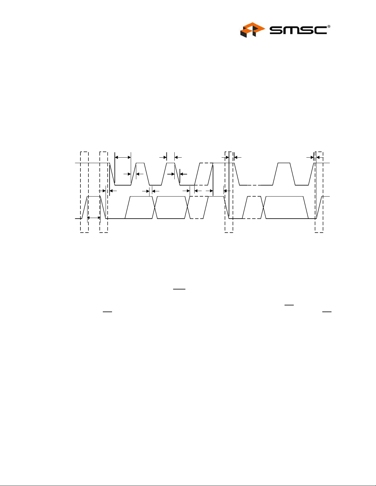
Figure 3.1 SMBus Timing Diagram
3.1.1 SMBus Start Bit
The SMBus Start bit is defined as a transition of the SMBus Data line from a logic ‘1’ state to a logic
‘0’ state while the SMBus Clock line is in a logic ‘1’ state.
3.1.2 SMBus Address and RD / WR Bit
The SMBus Address Byte consists of the 7-bit client address followed by a RD / WR
this RD / WR
bit is a logic ‘1’, then the SMBus Host is reading data from the client device.
The SMBus client will respond to one of multiple SMBus a ddresses determined by the pull-up resistor
on the ADDR_SEL pin. The ADDR_SEL pin decodes one of six pull-up resistors upon device power
up. Depending on the resistor used, the CLK pin may also be used to select a dditional functionality.
bit is a logic ‘0’, then the SMBus Host is writing data to the client device. If this RD / WR
indicator bit. If
SMSC EMC2305 13 Revision 1.3 (05-18-11)
DATASHEET
Multiple RPM-Based PWM Fan Controller for Five Fans
Datasheet
T able 3.1 ADDR_SEL Pin Decode
PULL-UP RESISTOR SMBUS ADDRESS ADDITIONAL FUNCTIONS
4.7k Ohm ±5% 0101_110(r/w)
6.8k Ohm ±5% 0101_111(r/w)
10k Ohm ±5% 0101_100(r/w)
15k Ohm ±5% 0101_101(r/w)
22k Ohm ±5% 1001_100(r/w)
None - CLK pin used as clock input
or output
33k Ohm ±5% 1001_101(r/w) CLK pin used to determine default
3.1.3 SMBus Data Bytes
All SMBus Data bytes are sent most significant bit first and composed of 8-bits of information.
3.1.4 SMBus ACK and NACK Bits
The SMBus client will acknowledge all data bytes that it receives (as well as the client add ress if it
matches and the ARA address if the ALERT# pin is asserted). This is done by the client device pulling
the SMBus Data line low after the 8th bit of each byte that is transmitted.
The Host will NACK (not acknowledge) the data received from the client by holding the SMBus data
line high after the 8th data bit has been sent.
3.1.5 SMBus Stop Bit
The SMBus Stop bit is defined as a transition of the SMBus Data line from a logic ‘0’ state to a logic
‘1’ state while the SMBus clock line is in a logic ‘1’ state. When the EMC2305 detects an SMBus Stop
bit has been communicating with the SMBus protocol, it will reset its client interface and prepare to
receive further communications.
3.1.6 SMBus Time-out
fan drive - see
CLK pin cannot be used as a clock
input or output
Section 4.5.1. The
The EMC2305 includes an SMBus timeout feature. Following a 30ms period of inactivity on the
SMBus, the device will time-out and reset the SMBus interface.
The SMBus timeout feature is disabled by default and can be en abled via clearing the DIS_TO bit in
the Configuration register (20h).
3.1.7 SMBus and I2C Compliance
The major difference between SMBus and I2C devices is highlighted here. For complete compliance
information refer to the SMBus 2.0 specification.
2
1. Minimum frequency for SMBus communications is 10kHz (I
2. The sla ve protocol will reset if the clock is held low for longer than 30ms (I2C has no timeout).
3. Th e slave protocol will reset if both the clock and data lines are held high for longer tha n 150us.
2
C devices do not support the Alert Response Address functionality (which is op tiona l for SMBus).
4. I
Revision 1.3 (05-18-11) 14 SMSC EMC2305
C has no minimum frequency).
DATASHEET
Multiple RPM-Based PWM Fan Controller for Five Fans
Datasheet
5. Th e Block Read and Block Write protocols are only compliant with I2C data formatting. They do
not support SMBus formatting for Block Read and Block Write protocols.
3.2 SMBus Protocols
The EMC2305 is SMBus 2.0 compatible and supports Send Byte, Read Byte, Receive Byte and Write
Byte as valid protocols as shown below. It will respond to the Alert Response Address protocol but is
not in full compliance.
All of the below protocols use the convention in
Table 3.2. When reading the protocol blocks, th e value
of YYYY_YYYb should be replaced with the respective SMBus addresses.
Table 3.2 Protocol Format
DATA SENT
TO DEVICE
DATA SENT TO
THE HOST
# of bits sent # of bits sent
3.2.1 Write Byte
The Write Byte is used to write one byte of data to the registers as shown below Table 3.3.
Table 3.3 Write Byte Protocol
ST ART
SLAVE
ADDRESS WR
ACK
REGISTER
ADDRESS ACK
REGISTER
DATA ACK STOP
1 -> 0 YYYY_YYYb 0 0 XXh 0 XXh 0 0 -> 1
3.2.2 Read Byte
The Read Byte protocol is used to read one byte of data from the registers as show n in
Table 3.4.
Table 3.4 Read Byte Protocol
START SLAVE
1 -> 0 YYYY_YYYb 0 0 XXh 0 0 -> 1 YYYY_YYYb 1 0 XXh 1 0 -> 1
ADDRESS
ACK Register
WR
Address
ACK START Slave
Address
RD ACK Register
Data
NACK STOP
3.2.3 Send Byte
The Send Byte protocol is used to set the internal address register pointer to the correct address
location. No data is transferred during the Send Byte protocol as shown in
Table 3.5.
Table 3.5 Send Byte Protocol
START
SLA VE
ADDRESS WR ACK
REGISTER
ADDRESS ACK STOP
1 -> 0 YYYY_YYYb 0 0 XXh 0 0 -> 1
SMSC EMC2305 15 Revision 1.3 (05-18-11)
DATASHEET
3.2.4 Receive Byte
The Receive Byte protocol is used to read data from a register when the internal register address
pointer is known to be at the right location (e.g. set via Send Byte). This is used for consecutive reads
of the same register as shown in
Multiple RPM-Based PWM Fan Controller for Five Fans
Datasheet
Table 3.6.
Table 3.6 Receive Byte Protocol
START
ADDRESS RD
ACK REGISTER DATA NACK STOP
1 -> 0 YYYY_YYYb 1 0 XXh 1 0 -> 1
3.2.5 Block Write Protocol
SLA VE
The Block Write is used to write multiple data bytes to a group of contiguous registers as shown in
Table 3.7. It is an extension of the Write Byte Protocol.
Table 3.7 Block Write Protocol
START
SLAVE
ADDRESS WR ACK
REGISTER
ADDRESS ACK
REGISTER
DATA ACK
1 ->0 YYYY_YYYb 0 0 XXh 0 XXh 0
REGISTER
DATA
ACK
REGISTER
DATA ACK . . .
REGISTER
DATA ACK STOP
XXh 0 XXh 0 . . . XXh 0 0 -> 1
3.2.6 Block Read Protocol
The Block Read is used to read multiple data bytes from a group of contiguous registers as sh own in
Table 3.8. It is an extension of the Read Byte Protocol.
Table 3.8 Block Read Protocol
START SLAVE
ADDRESS
WR
ACK REGISTER
ADDRESS
ACK START SLAVE
ADDRESS
RD ACK REGISTER
DATA
1->0 YYYY_YYYb 0 0 XXh 0 1 ->0 YYYY_YYYb 1 0 XXh
ACK
REGISTER
DATA
ACK REGISTER
DATA
ACK REGISTER
DATA
ACK . . . REGISTER
DATA
NACK STOP
0 XXh 0 XXh 0 XXh 0 . . . XXh 1 0 -> 1
3.2.7 Alert Response Address
The ALERT# output can be used as a processor interrupt or as an SMBus Alert when configured to
operate as an interrupt.
When it detects that the ALERT# pin is asserted, the host will send the Alert Response Address (ARA)
to the general address of 0001_100xb. All devices with active i nterrupts will respond with their client
address as shown in
Revision 1.3 (05-18-11) 16 SMSC EMC2305
Table 3.9.
DATASHEET
Multiple RPM-Based PWM Fan Controller for Five Fans
Datasheet
Table 3.9 Alert Response Address Protocol
ALERT
START
RESPONSE
ADDRESS RD
ACK
DEVICE
ADDRESS NACK STOP
1 -> 0 0001_100b 1 0 YYYY_YYYb 1 0 -> 1
The EMC2305 will respond to the ARA in the following way if the ALERT# pin is asserted.
1. Send Slave Address and verify that full slav e address was sent (i.e. the SMBus communication
from the device was not prematurely stopped due to a bus contention event).
2. Set the MASK bit to clear the ALERT# pin.
SMSC EMC2305 17 Revision 1.3 (05-18-11)
DATASHEET
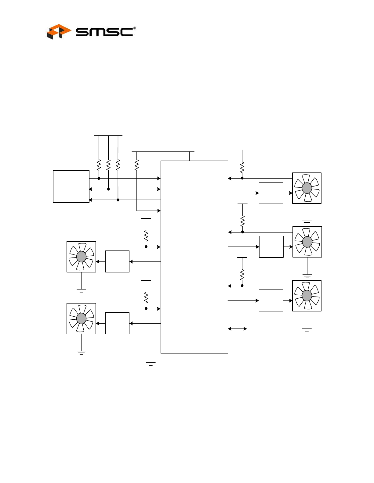
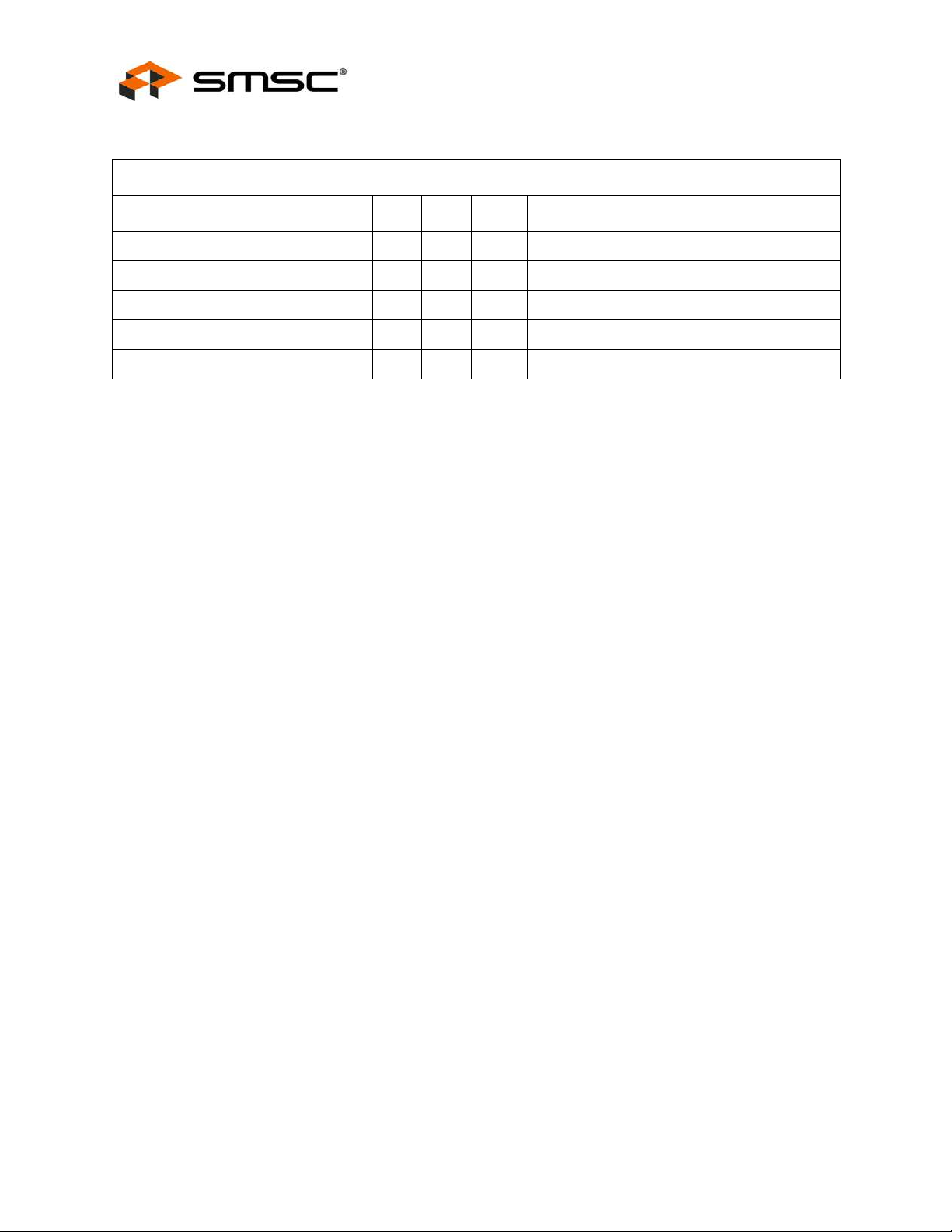
Chapter 4 Product Description
EMC 2305
SMCLK
SMDATA
ALERT#
VDD
3.3V
MCU
ADDR_SEL
GND
32.768KHz Clock
Input or O utput
CLK
TACH3
tachometer
PWM3
Drive
Circuit
TACH4
tachometer
PWM4
Drive
Circuit
TACH5
tachometer
PWM5
Drive
Circuit
TACH1
tachometer
PWM1
Drive
Circuit
TACH2
tachometer
PWM2
Drive
Circuit
The EMC2305 is an SMBus compliant fan controller with five programmable frequency PWM fan
drivers. The fan drivers can be operated using two modes: the RPM-based Fan Speed Control
Algorithm or the direct fan drive setting.
Figure 4.1 shows a system diagram of the EMC2305.
Multiple RPM-Based PWM Fan Controller for Five Fans
Datasheet
4.1 Fan Control Modes of Operation
The EMC2305 has two modes of operation for each fan driver. Each mode of operation uses the Ramp
Revision 1.3 (05-18-11) 18 SMSC EMC2305
Rate control and Spin Up Routine.
1. Direct Setting Mode - in this mode of operation, the user directly controls the fan drive setting.
Updating the Fan Driver Setting Register (see
Ramp Rate control is optional and enabled via the EN_RRC b its.
Figure 4.1 System Diagram of EMC2305
DATASHEET
Section 5.7) will instantly update the PWM fan drive.
 Loading...