

Page 1

COM20020 ULANC
Universal Local Area Network Controller
with 2K x 8 On-Board RAM
• 24-Pin Embedded Network Controller/
Transceiver/RAM
• Ideal for Industrial/Factory Automation
and Automotive Applications
• Deterministic, 2.5 Mbps, Token Passing
ARCNET Protocol
• Minimal Microcontroller and Media
Interface Logic Required
• Flexible Microcontroller Interface for Use
with 80XX, 68XX, etc.
• Automatically Detects Type of
Microcontroller Interface:
- Non-Multiplexed or Multiplexed Bus
- Separate nRD & nWR Lines or DIR &
nDS Lines
• Full 2Kx8 On-Chip RAM
• Command Chaining for Top Performance
• Reduced Reconfiguration Times
• Sequential Access to Internal RAM
• Software Programmable Node ID
• Duplicate Node ID Detection
• Powerful Diagnostics
• Receive All Mode
COM20020
FEATURES
• Data Rates from 2.5 Mbps to 156.25 Kbps
• 24-Pin DIP or 28-Pin PLCC Package
• Flexible Media Interface:
- Traditional Hybrid Interface for Long
Distances
- RS485 Differential Driver Interface for
Low Cost, Low Power, High Reliability
- Backplane Mode for Direct Connection to
Media in Short Distance Applications
• Eight, 256-Byte Pages Allow 4 Pages TX
and RX Plus Scratch-Pad Memory
• No Wait-State Arbitration
• Programmable TXEN Polarity
• Next ID Readable
• Internal Clock Prescaler for Slower Network
Speed without Slowing Arbitration
• Operating Temperature Range of -40oC to
+85oC, or 0oC to +70oC
• Self-Reconfiguration Protocol
• Supports up to 255 Nodes
• Supports Various Network Topologies (Star,
Tree, Bus...)
• CMOS, Single +5V Supply
GENERAL DESCRIPTION
SMSC's COM20020 is a member of the family
of Industrial Network Controllers from Standard
Microsystems Corporation. The device is a
special purpose communications controller for
networking microcontrollers and intelligent
peripherals in industrial, automotive, and
embedded control environments using an
ARCNET® protocol engine. The small 24-pin
package, flexible microcontroller and media
interfaces, eight-page message support, and
extended temperature range of the COM20020
make it the only true network
Page 2

2
TABLE OF CONTENTS
FEATURES........................................................................................................................................1
GENERAL DESCRIPTION .................................................................................................................1
PIN CONFIGURATION.......................................................................................................................3
DESCRIPTION OF PIN FUNCTIONS .................................................................................................4
PROTOCOL DESCRIPTION ..............................................................................................................8
NETWORK PROTOCOL ....................................................................................................................8
DATA RATES.....................................................................................................................................8
NETWORK RECONFIGURATION......................................................................................................8
BROADCAST MESSAGES.................................................................................................................9
EXTENDED TIMEOUT FUNCTION.....................................................................................................9
LINE PROTOCOL ............................................................................................................................10
SYSTEM DESCRIPTION ..................................................................................................................12
MICROCONTROLLER INTERFACE.................................................................................................12
TRANSMISSION MEDIA INTERFACE..............................................................................................15
FUNCTIONAL DESCRIPTION.......................................................................................................... 19
MICROSEQUENCER .......................................................................................................................19
INTERNAL REGISTERS................................................................................................................... 22
INTERNAL RAM...............................................................................................................................32
COMMAND CHAINING.....................................................................................................................37
INITIALIZATION SEQUENCE...........................................................................................................40
IMPROVED DIAGNOSTICS .............................................................................................................40
OPERATIONAL DESCRIPTION.......................................................................................................43
MAXIMUM GUARANTEED RATINGS*..............................................................................................43
DC ELECTRICAL CHARACTERISTICS............................................................................................43
TIMING DIAGRAMS ........................................................................................................................46
COM20020 ERRATA SHEET...........................................................................................................59
For more details on the ARCNET protocol engine and traditional dipulse signalling schemes,
please refer to the ARCNET Local Area Network Standard, available from Standard
Microsystems Corporation or the ARCNET Designer's Handbook, available from Datapoint
Corporation.
For more detailed information on cabling options including RS485, transformer-coupled RS485 and Fiber Optic interfaces, please refer to the following technical note which is available
from Standard Microsystems Corporation: Technical Note 7-5 - Cabling Guidelines for the
COM20020 ULANC.
Page 3

3
controller optimized for use in industrial and
A0/nMUX
n
C
S
n
I
N
T
R
n
R
E
S
E
T
I
N
V
S
S
n
T
X
E
N
R
X
I
N
n
P
U
L
S
E
2
A
D
1
V
S
S
A
D
2
D3D4D5D
6
automotive applications. Using an ARCNET
protocol engine is the ideal solution for factory
automation applications because it provides a
token-passing protocol, a highly reliable and
proven networking scheme, and a data rate of
up to 2.5 Mbps when using the COM20020.
A token-passing protocol provides predictable
response times because each network event
occurs within a predetermined time interval,
based upon the number of nodes on the
PIN CONFIGURATION
VDD
24
23
nRD/nDS
22
nWR/DIR
nCS
21
nINTR
20
19
nRESET IN
18
nTXEN
17
RXIN
nPULSE2
16
15
nPULSE1
14
XTAL2
13
XTAL1
A2/ALE
AD0
AD1
AD2
VSS
1
2
A1
3
4
5
6
D3
7
D4
8
D5
9
10
D6
11
D7
12
network. The deterministic nature of ARCNET
is essential in mission critical applications.
The integration of the 2Kx8 RAM buffer on-chip,
the Command Chaining feature, the 2.5 Mbps
maximum data rate, and the internal diagnostics
make the COM20020 the highest performance
industrial communications device available.
With only one COM20020 and one
microcontroller, a complete communications
node may be implemented.
ARCNET is a registered trademark of Datapoint Corporation
nWR/DIR
nRD/nDS
VDD
A0/nMUX
A1
A2/ALE
AD0
25 24 23 22 21 20 19
26
27
28
1
2
3
4
5 6 7 8 9 10 11
18
17
16
15
14
13
12
nPULSE 1
XTAL2
XTAL1
VDD
VSS
N/C
D7
Packages: 24-Pin DIP or 28-Pin PLCC
Ordering Information:
COM20020 P
PACKAGE TYPE: P = Plastic, LJP = PLCC
TEMP RANGE: (Blank) = Commercial: 0°C to +70°C
I = Industrial: -40°C to +85°C
DEVICE TYPE: 20020 = Universal Local Area Network Controller
(with 2K x 8 RAM)
Page 4

4
DESCRIPTION OF PIN FUNCTIONS
DIP PIN
NO.
1-3 1-3 Address
4-11 4-6,8-12 Data 0-7 AD0-AD2,
23 27 nRead/nData
22 26 nWrite/
PLCC PIN
NO.
NAME
MICROCONTROLLER INTERFACE
0-2
nStrobe
Direction
SYMBOL DESCRIPTION
A0/nMUX,
A1,A2/ALE
D3-D7
nRD/nDS Input. On a 68XX-like bus, this active low
nWR/DIR Input. On a 68XX-like bus, this signal is
Input. On a non-multiplexed bus, these
signals are directly connected to the low bits
of the host address bus. On a multiplexed
address/data bus, A0/nMUX is tied low, A1
is left open, and A2 is tied to the Address
Latch Enable signal of the host. A1 is
connected to an internal pull-up resistor.
Input/Output. On a non-multiplexed bus,
these signals are used as the data lines for
the device. On a multiplexed address/data
bus, AD0-AD2 act as the address lines
(latched by ALE) and as the low data lines
for the device. D3-D7 are always used for
data only. These signals are connected to
internal pull-up resistors.
signal is issued by the microcontroller as the
data strobe signal to strobe the data onto
the bus. On a 80XX-like bus, this active low
signal is issued by the microcontroller to
indicate a read operation. In this case, a
logic "0" on this pin, when the COM20020 is
accessed, enables data from the device to
the data bus to be read by the
microcontroller.
issued by the microcontroller as the
Read/nWrite signal to determine the
direction of data transfer. In this case, a
logic "1" selects a read operation, while a
logic "0" selects a write operation. In this
case, data is actually strobed by the nDS
signal. On an 80XX-like bus, this active low
signal is issued by the microcontroller to
indicate a write operation. In this case, a
logic "0" on this pin, when the COM20020 is
accessed, enables data from the data bus to
be written to the device.
Page 5

5
DIP PIN
NO.
PLCC PIN
NO.
NAME
SYMBOL DESCRIPTION
19 23 nReset in nRESET IN Input. This active low signal issued by the
microcontroller executes a hardware reset.
It is used to activate the internal reset
circuitry within the COM20020.
20 24 nInterrupt nINTR Output. This active low signal is generated
by the COM20020 when an enabled
interrupt condition occurs. nINTR returns to
its inactive state when the interrupt status
condition or the corresponding interrupt
mask bit is reset.
21 25 nChip Select nCS Input. This active low signal issued by the
microcontroller selects the COM20020 for
an access.
TRANSMISSION MEDIA INTERFACE
16,15 19,18 nPulse 2,
nPulse 1
nPULSE2,
nPULSE1
Output. In Normal Mode, these active low
signals carry the transmit data information,
encoded in pulse format, from the
COM20020 to the media driver circuitry.
When the device is in Backplane Mode, the
nPULSE1 signal driver is programmable
(push/pull or open-drain), while the
nPULSE2 signal provides a clock with
frequency of crystal/4. nPULSE1 is
connected to a weak internal pull-up resistor
in backplane mode.
17 20 Receive In RXIN Input. This signal carries the receive data
information from the line receiver circuitry to
the COM20020.
18 21 nTransmit
nEnable
nTXEN
Output. This signal is used prior to the
Power-up to enable the line drivers for
transmission. The polarity of the signal is
programmable by grounding the nPULSE2
pin.
nPULSE2 floating before Power-up: nTXEN
active low (Default option)
nPULSE2 grounded before Power-up:
nTXEN active high (This option is only
available in Backplane Mode)
MISCELLANEOUS
13,14 16,17 Crystal
Oscillator
XTAL1,
XTAL2
An external crystal should be connected to
these pins. If an external TTL clock is used
Page 6

6
DIP PIN
NO.
PLCC PIN
NO.
NAME
24 15,28 Power
Supply
12 7,14,22 Ground V
SYMBOL DESCRIPTION
instead, it must be connected to XTAL1 with
a 390Ω pull-up resistor, and XTAL2 should
be left floating.
V
DD
SS
+5 Volt Power Supply pin.
Ground pin.
Page 7

7
SEND ACK
Reconfigure
Timer has
Timed Out
Power On
Send
Reconfigure
Burst
Read Node ID
Write ID to
RAM Buffer
Set NID=ID
1
Start
Reconfiguration
Timer (840 mS)
YN
TA?
Broadcast?
Y
Send
Packet
Was Packet
Broadcast?
N
No
Y
Activity
for 74.7
us?
N
N
ID refers to the identification number of the ID assigned to this node.
NID refers to the next identification number that receives the token after
after this ID passes it.
SID refers to the source identification.
DID refers to the destination identification.
SOH refers to the start of header character; preceeds all data packets.
-
Y
ACK? Set TMA
Y
Invitation
to Transmit to
this ID?
Transmit
NAK
Transmit
ACK
N
Y
Set TA
Y N
RI?
Free Buffer
Increment
N
Y N
Free Buffer
Enquiry to
this ID?
Transmit
Enquiry
N
Y N
ACK?
Y
NAK?
NID
No
Activity
for 74.7
us?
N
No
Activity
for 74.7
us?
Y N
SOH?
NY
RI?
Write SID
to Buffer
Y
Pass the
Token
DID
=0?
N
DID
=ID?
Y
Write Buffer
with Packet
CRC
OK?
Y
LENGTH
OK?
Y
DID
=0?
N
DID
=ID?
Y
Broadcast
Enabled?
N
N
N
Y
N
N
Y
Set RI
Y
Set TA
1
NY
No Activity
for 82
uS?
Set NID=ID
Start Timer:
T=(255-ID)
x 146 us
Activity
On Line?
N
T=0?
N
Y
Y
N
Y
FIGURE 1 - COM20020 OPERATION
Page 8

8
PROTOCOL DESCRIPTION
NETWORK PROTOCOL
Communication on the network is based on a
token passing protocol. Establishment of the
network configuration and management of the
network protocol are handled entirely by the
COM20020's internal microcoded sequencer. A
processor or intelligent peripheral transmits data
by simply loading a data packet and its
destination ID into the COM20020's internal
RAM buffer, and issuing a command to enable
the transmitter. When the COM20020 next
receives the token, it verifies that the receiving
node is ready by first transmitting a FREE
BUFFER ENQUIRY message. If the receiving
node transmits an ACKnowledge message, the
data packet is transmitted followed by a 16-bit
CRC. If the receiving node cannot accept the
packet (typically its receiver is inhibited), it
transmits a Negative AcKnowledge message
and the transmitter passes the token. Once it
has been established that the receiving node
can accept the packet and transmission is
complete, the receiving node verifies the packet.
If the packet is received successfully, the
receiving node transmits an ACKnowledge
message (or nothing if it is not received
successfully) allowing the transmitter to set the
appropriate status bits to indicate successful or
unsuccessful delivery of the packet. An interrupt
mask permits the COM20020 to generate an
interrupt to the processor when selected status
bits become true. Figure 1 is a flow chart
illustrating the internal operation of the
COM20020 connected to a 20 MHz crystal
oscillator.
DATA RATES
The COM20020 is capable of supporting data
rates from 156.25 Kbps to 2.5 Mbps. The
following protocol description assumes a 2.5
Mbps data rate. For slower data rates, an
internal clock divider scales down the clock
frequency. Thus all timeout values are scaled
up as shown in the following table:
TIMEOUT
SCALING
FACTOR
(MULTIPLY BY)
1
2
4
8
16
CLOCK
PRESCALER
÷8
÷16
÷32
÷64
÷128
DATA RATE
W/20MHz
XTAL
2.5 Mbps
1.25 Mbps
625 Kbps
312.5 Kbps
156.25 Kbps
Example: IDLE LINE Timeout @ 2.5 Mbps = 82
µs. IDLE LINE Timeout for 156.2 Kbps is 82 µs
* 16 = 1.3 ms
NETWORK RECONFIGURATION
A significant advantage of the COM20020 is its
ability to adapt to changes on the network.
Whenever a new node is activated or
deactivated, a NETWORK
RECONFIGURATION is performed. When a
new COM20020 is turned on (creating a new
active node on the network), or if the
COM20020 has not received an INVITATION
TO TRANSMIT for 840mS, or if a software reset
occurs, the COM20020 causes a NETWORK
RECONFIGURATION by sending a
RECONFIGURE BURST consisting of eight
marks and one space repeated 765 times. The
purpose of this burst is to terminate all activity
on the network. Since this burst is longer than
any other type of transmission, the burst will
interfere with the next INVITATION TO
TRANSMIT, destroy the token and keep any
other node from assuming control of the line.
Page 9

9
When any COM20020 senses an idle line for
greater than 82µS, which occurs only when the
token is lost, each COM20020 starts an internal
timeout equal to 146µs times the quantity 255
minus its own ID. The COM20020 starts
network reconfiguration by sending an invitation
to transmit first to itself and then to all other
nodes by decrementing the destination Node ID.
If the timeout expires with no line activity, the
COM20020 starts sending INVITATION TO
TRANSMIT with the Destination ID (DID) equal
to the currently stored NID. Within a given
network, only one COM20020 will timeout (the
one with the highest ID number). After sending
the INVITATION TO TRANSMIT, the
COM20020 waits for activity on the line. If there
is no activity for 74.7µS, the COM20020
increments the NID value and transmits another
INVITATION TO TRANSMIT using the NID
equal to the DID. If activity appears before the
74.7µS timeout expires, the COM20020 releases
control of the line. During NETWORK
RECONFIGURATION, INVITATIONS TO
TRANSMIT are sent to all NIDs (1-255).
Each COM20020 on the network will finally have
saved a NID value equal to the ID of the
COM20020 that it released control to. At this
point, control is passed directly from one node
to the next with no wasted INVITATIONS TO
TRANSMIT being sent to ID's not on the
network, until the next NETWORK
RECONFIGURATION occurs. When a node is
powered off, the previous node attempts to pass
the token to it by issuing an INVITATION TO
TRANSMIT. Since this node does not respond,
the previous node times out and transmits
another INVITATION TO TRANSMIT to an
incremented ID and eventually a response will
be received.
The NETWORK RECONFIGURATION time
depends on the number of nodes in the network,
the propagation delay between nodes, and the
highest ID number on the network, but is
typically within the range of 24 to 61 ms.
BROADCAST MESSAGES
Broadcasting gives a particular node the ability
to transmit a data packet to all nodes on the
network simultaneously. ID zero is reserved for
this feature and no node on the network can be
assigned ID zero. To broadcast a message, the
transmitting node's processor simply loads the
RAM buffer with the data packet and sets the
DID equal to zero. Figure 8 illustrates the
position of each byte in the packet with the DID
residing at address 0X01 or 1 Hex of the
current page selected in the "Enable Transmit
from Page fnn" command. Each individual node
has the ability to ignore broadcast messages by
setting the most significant bit of the "Enable
Receive to Page fnn" command (see Table 6) to
a logic "0".
EXTENDED TIMEOUT FUNCTION
There are three timeouts associated with the
COM20020 operation. The values of these
timeouts are controlled by bits 3 and 4 of the
Configuration Register and bit 5 of the Setup
Register.
Response Time
The Response Time determines the maximum
propagation delay allowed between any two
nodes, and should be chosen to be larger than
the round trip propagation delay between the
two furthest nodes on the network plus the
maximum turn around time (the time it takes a
particular COM20020 to start sending a
message in response to a received message)
which is approximately 12.7µS. The round trip
propagation delay is a function of the
transmission media and network topology. For
a typical system using RG62 coax in a
baseband system, a one way cable propagation
delay of 31µS translates to a distance of about 4
miles. The flow chart in Figure 1 uses a value
of 74.7µS (31 + 31 + 12.7) to determine if any
node will respond.
Page 10

10
Idle Time
The Idle Time is associated with a NETWORK
RECONFIGURATION. Figure 1 illustrates that
during a NETWORK RECONFIGURATION one
node will continually transmit INVITATIONS TO
TRANSMIT until it encounters an active node.
All other nodes on the network must distinguish
between this operation and an entirely idle line.
During NETWORK RECONFIGURATION,
activity will appear on the line every 82µS. This
82µS is equal to the Response Time of 74.7µS
plus the time it takes the COM20020 to start
retransmitting another message (usually another
INVITATION TO TRANSMIT).
Reconfiguration Time
Unlike asynchronous protocols, there is a
constant amount of time separating each data
byte. On a 2.5 Mbps network, each byte takes
exactly 11 clock intervals of 400ns each. As a
result, one byte is transmitted every 4.4µS and
the time to transmit a message can be precisely
determined. The line idles in a spacing (logic
"0") condition. A logic "0" is defined as no line
activity and a logic "1" is defined as a negative
pulse of 200nS duration. A transmission starts
with an ALERT BURST consisting of 6 unit
intervals of mark (logic "1"). Eight bit data
characters are then sent, with each character
preceded by 2 unit intervals of mark and one
unit interval of space. Five types of
transmission can be performed as described
below:
If any node does not receive the token within the
Reconfiguration Time, the node will initiate a
NETWORK RECONFIGURATION. The ET2
and ET1 bits of the Configuration Register allow
the network to operate over longer distances
than the 4 miles stated earlier. The logic levels
on these bits control the maximum distances
over which the COM20020 can operate by
controlling the three timeout values described
above. For proper network operation, all
COM20020's connected to the same network
must have the same Response Time, Idle Time,
and Reconfiguration Time.
LINE PROTOCOL
The ARCNET line protocol is considered
isochronous because each byte is preceded by a
start interval and ended with a stop interval.
Invitations To Transmit
An Invitation To Transmit is used to pass the
token from one node to another and is sent by
the following sequence:
• An ALERT BURST
• An EOT (End Of Transmission: ASCII code
04H)
• Two (repeated) DID (Destination
ID) characters
ALERT
Free Buffer Enquiries
A Free Buffer Enquiry is used to ask another
node if it is able to accept a packet of data. It is
sent by the following sequence:
• An ALERT BURST
• An ENQ (ENQuiry: ASCII code 85H)
• Two (repeated) DID (Destination ID)
characters
ALERT
Page 11

11
Data Packets
ALE
R
T
BUR
S
T
SOH
SID
DID
DID
COU
N
T
dat
a
dat
a
CRC
CRC
A Data Packet consists of the actual data being
sent to another node. It is sent by the following
sequence:
• An ALERT BURST
• An SOH (Start Of Header--ASCII code 01H)
• An SID (Source ID) character
• Two (repeated) DID (Destination ID)
characters
• A single COUNT character which is the 2's
complement of the number of data bytes to
follow if a short packet is sent, or 00H
followed by a COUNT character if a long
packet is sent
• N data bytes where COUNT = 256-N (or 512N for a long packet)
• Two CRC (Cyclic Redundancy Check)
characters. The CRC polynomial used is:
X16 + X15 + X2 + 1.
Acknowledgements
An Acknowledgement is used to acknowledge
reception of a packet or as an affirmative
response to FREE BUFFER ENQUIRIES and is
sent by the following sequence:
• An ALERT BURST
• An ACK (ACKnowledgement--ASCII code
86H) character
ALERT
ACK
BURST
Negative Acknowledgements
A Negative Acknowledgement is used as a
negative response to FREE BUFFER
ENQUIRIES and is sent by the following
sequence:
• An ALERT BURST
• A NAK (Negative Acknowledgement--ASCII
code 15H) character
ALERT
NAK
BURST
Page 12

12
SYSTEM DESCRIPTION
MICROCONTROLLER INTERFACE
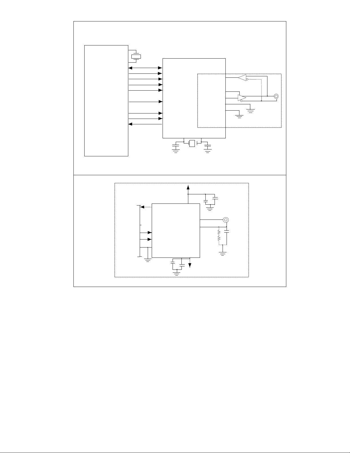
The top halves of Figures 2 and 3 illustrate
typical COM20020 interfaces to the
microcontrollers. The interfaces consist of an 8bit data bus, an address bus, and a control bus.
In order to support a wide range of
microcontrollers without requiring glue logic and
without increasing the number of pins, the
COM20020 automatically detects and adapts to
the type of microcontroller being used. Upon
hardware reset, the COM20020 first determines
whether the read and write control signals are
separate READ and WRITE signals (like the
80XX) or DIRECTION and DATA STROBE (like
the 68XX). To determine the type of control
signals, the device requires the software to
execute at least one write access to external
memory before attempting to access the
COM20020. The device defaults to 80XX-like
signals. Once the type of control signals are
determined, the COM20020 remains in this
interface mode until the next hardware reset
occurs. The second determination the
COM20020 makes is whether the bus is
multiplexed or non-multiplexed. To determine
the type of bus, the device requires the software
to write to an odd memory location followed by a
read from an odd location before attempting to
access the COM20020. The signal on the A0
pin during the odd location access tells the
COM20020 the type of bus. Since multiplexed
operation requires A0 to be active low, activity
on the A0 line tells the COM20020 that the bus
is non-multiplexed. The device defaults to
multiplexed operation. Both determinations may
be made simultaneously by performing a
WRITE followed by a READ operation to an odd
location within the COM20020 Address space
20020 registers. Once the type of bus is
determined, the COM20020 remains in this
interface mode until hardware reset occurs.
Whenever nCS and nRD are activated, the
preset determinations are assumed as final and
will not be changed until hardware reset.
Refer to Description of Pin
Functions section for details on the related
signals. All accesses to the internal RAM and
the internal registers are controlled by the
COM20020. The internal RAM is accessed via
a pointer-based scheme (refer to the Sequential
Access Memory section), and the internal
registers are accessed via direct addressing.
Many peripherals are not fast enough to take
advantage of high-speed microcontrollers. Since
microcontrollers do not typically have READY
inputs, standard peripherals cannot extend
cycles to extend the access time. The access
time of the COM20020, on the other hand, is so
fast that it does not need to limit the speed of
the microcontroller. The COM20020 is
designed to be flexible so that it is independent
of the microcontroller speed.
The COM20020 provides for no wait state
arbitration via direct addressing to its internal
registers and a pointer based addressing
scheme to access its internal RAM. The pointer
may be used in auto-increment mode for typical
sequential buffer emptying or loading, or it can
be taken out of auto-increment mode to perform
random accesses to the RAM. The data within
the RAM is accessed through the data register.
Data being read is prefetched from memory and
placed into the data register for the
microcontroller to read. It is important to notice
that only by writing a new address pointer
(writing to an address pointer low), one obtains
the contents of COM20020 internal RAM.
Performing only read from the Data Register
does not load new data from the internal RAM.
During a write operation, the data is stored in
the data register and then written into memory.
Whenever the pointer is loaded for reads with a
new value, data is immediately prefetched to
prepare for the first read operation.
Page 13

13
XTAL1
XTA
L
1
XTA
L
2
COM20020
XTAL2
AD0-AD7
ALE
A15
RESET
nRD
nWR
nINT1
8051
AD0-AD2, D3-D7
A2/BALE
nCS
nRESET IN
nRD/nDS
nWR/DIR
nINTR
A0/nMUX
27 pF
RXIN
nTXEN
nPULSE1
nPULSE2
GND
27 pF
75176B or
Equiv.
Differential Driver
Configuration
Media Interface
*
may be replaced
with Figure A, B or C.
FIGURE 2 - MULTIPLEXED, 8051-LIKE BUS INTERFACE WITH RS-485 INTERFACE
+5V
RXIN
TXEN
nPULSE1
nPULSE2
GND
+5V
100 Ohm
RXIN
nPULSE1
+5V
2
Receiver
6
HFD3212-002
7
Transmitter
HFE4211-014
3
2
6
7
BACKPLANE CONFIGURATION
FIGURE A
2 Fiber Interface
(ST Connectors)
NOTE: COM20020 must be in backplane mode
FIGURE B
Page 14
14
+
FIGURE C
XTA
L
1
XTA
L
2
6801
20M
H
z
XTAL
XTAL1
XTAL2
D0-D7
nRES
nIOS
R/nW
nIRQ1
A0
A1
A2
A7
D0-D7
A0/nMUX
A1
A2/BALE
nCS
nRESET IN
nRD/nDS
nWR/nDIR
nINTR
27 pF
COM20020
RXIN
TXEN
nPULSE1
nPULSE2
GND
27 pF
75176B or
Equiv.
Differential Driver
Configuration
Media Interface
*
may be replaced
with Figure A, B or C.
FIGURE 3 - NON-MULTIPLEXED, 6801-LIKE BUS INTERFACE WITH RS-485 INTERFACE
+5V
RXIN
HYC9068 or
HYC9088
RXIN
10
uF
6
0.47
uF
nTXEN
nPULSE1
nPULSE2
GND
N/C
nPULSE1
nPULSE2
17, 19,
4, 13, 14
0.47
uF
12
11
5.6K
1/2W
5.6K
1/2W
3
+
10
uF
-5V
Traditional Hybrid
Configuration
0.01 uF
1KV
Page 15

15
TRANSMISSION MEDIA INTERFACE
reception of data consisting of 1, 1, 0.
The bottom halves of Figures 2 and 3 illustrate
the COM20020 interface to the transmission
media used to connect the node to the network.
Table 1 lists different types of cable which are
suitable for ARCNET applications.1 The user
may interface to the cable of choice in one of
three ways:
Traditional Hybrid Interface
The Traditional Hybrid Interface is that which is
used with previous ARCNET devices. The
Hybrid Interface is recommended if the node is
to be placed in a network with other HybridInterfaced nodes. The Traditional Hybrid
Interface is for use with nodes operating at 2.5
Mbps only. The transformer coupling of the
Hybrid offers isolation for the safety of the
system and offers high Common Mode
Rejection. The Traditional Hybrid Interface uses
circuits like SMSC's HYC9068 or HYC9088 to
transfer the pulse-encoded data between the
cable and the COM20020. The COM20020
transmits a logic "1" by generating two 100nS
non-overlapping negative pulses, nPULSE1 and
nPULSE2. Lack of pulses indicates a logic "0".
The nPULSE1 and nPULSE2 signals are sent to
the Hybrid, which creates a 200nS dipulse
signal on the media. A logic "0" is transmitted
by the absence of the dipulse. During reception,
the 200nS dipulse appearing on the media is
coupled through the RF transformer of the LAN
Driver, which produces a positive pulse at the
RXIN pin of the COM20020. The pulse on the
RXIN pin represents a logic "1". Lack of pulse
represents a logic "0". Typically, RXIN pulses
occur at multiples of 400nS. The COM20020
can tolerate distortion of plus or minus 100nS
and still correctly capture and convert the RXIN
pulses to NRZ format. Figure 5 illustrates the
events which occur in transmission or
1
Please refer to TN7-5 - Cabling Guidelines
for the COM20020 ULANC, available from
SMSC, for recommended cabling distance,
termination, and node count for ARCNET nodes.
Backplane Configuration
The Backplane Open Drain Configuration is
recommended for cost-sensitive, short-distance
applications like backplanes and
instrumentation. This mode is advantageous
because it saves components, cost, and power.
Since the Backplane Configuration encodes
data differently than the traditional Hybrid
Configuration, nodes utilizing the Backplane
Configuration cannot communicate directly with
nodes utilizing the Traditional Hybrid
Configuration.
The Backplane Configuration does not isolate
the node from the media nor protects it from
Common Mode noise, but Common Mode Noise
is less of a problem in short distances.
The COM20020 supplies a programmable
output driver for Backplane Mode operation. A
push/pull or open drain driver can be selected
by programming the P1MODE bit of the Setup
Register (see register descriptions for details.)
The COM20020 defaults to an open drain
output.
The Backplane Configuration provides for direct
connection between the COM20020 and the
media. Only one pull-up resistor (in open drain
configuration of the output driver) is required
somewhere on the media (not on each
individual node). The nPULSE1 signal, in this
mode, is an open drain or push/pull driver and is
used to directly drive the media. It issues a
200nS negative pulse to transmit a logic "1". ote
that when used in the open-drain mode, the
COM20020 does not have a fail/safe input on
the RXIN pin. The nPULSE1 signal actually
contains a weak pull-up resistor. This pull-up
should not take the place of the resistor
required on the media for open drain mode.
Page 16

16
FIGURE 5 - DIPULSE WAVEFORM FOR DATA OF 1-1-0
RT RT
+VCC
+VCC +VCC
75176B or
RBIAS
RBIAS
RBIAS
Equiv.
COM20020 COM20020 COM20020
FIGURE 4 - COM20020 NETWORK USING RS-485 DIFFERENTIAL TRANSCEIVERS
20MHZ
CLOCK
(FOR REF.
ONLY)
nPULSE1
nPULSE2
DIPULSE
RXIN
100ns
1 0
100ns
200ns
400ns
1
Page 17

17
In typical applications, the serial backplane is
terminated at both ends and a bias is provided
by the external pull-up resistor.
The RXIN signal is directly connected to the
cable via an internal Schmitt trigger. A negative
pulse on this input indicates a logic "1". Lack of
pulse indicates a logic "0". For typical singleended backplane applications, RXIN is
connected to nPULSE1 to make the serial
backplane data line. A ground line (from the
coax or twisted pair) should run in parallel with
the signal. For applications requiring different
treatment of the receive signal (like filtering or
squelching), nPULSE1 and RXIN remain as
independent pins. External differential
drivers/receivers for increased range and
common mode noise rejection, for example,
would require the signals to be independent of
one another. When the device is in Backplane
Mode, the clock provided by the nPULSE2
signal may be used for encoding the data into a
different encoding scheme or other synchronous
operations needed on the serial data stream.
Differential Driver Configuration
The Differential Driver Configuration is a special
case of the Backplane Mode. It is a dc coupled
configuration recommended for applications like
car-area networks or other cost-sensitive
applications which do not require direct
compatibility with existing ARCNET nodes and
do not require isolation.
The Differential Driver Configuration cannot
communicate directly with nodes utilizing the
Traditional Hybrid Configuration. Like the
Backplane Configuration, the Differential Driver
Configuration does not isolate the node from the
media.
The Differential Driver interface includes a
RS485 Driver/Receiver to transfer the data
between the cable and the COM20020. The
nPULSE1 signal transmits the data, provided
the Transmit Enable signal is active. The
nPULSE1 signal issues a 200nS negative pulse
to transmit a logic "1". Lack of pulse indicates
a logic "0". The RXIN signal receives the data,
the transmitter portion of the COM20020 is
disabled during reset and the nPULSE1,
nPULSE2 and nTXEN pins are inactive.
Programmable TXEN Polarity
To accommodate transceivers with active high
ENABLE pins, the COM20020 contains a
programmable TXEN output. To program the
TXEN pin for an active high pulse, the nPULSE2
pin should be connected to ground. To retain
the normal active low polarity, nPULSE2 should
be left open. The polarity determination is made
at power on reset and is valid only for Backplane
Mode operation. The nPULSE2 pin should
remain grounded at all times if an active high
polarity is desired.
Page 18

18
AD0-AD2,
A0/
n
M
U
X
A
1
A2/
B
ALE
D3-D7
ADDRESS
DECODING
CIRCUITRY
2K x 8
RAM
ADDITIONAL
REGISTERS
nINTR
nRESET IN
nRD/nDS
nWR/DIR
nCS
STATUS/
COMMAND
REGISTER
RESET
LOGIC
BUS
ARBITRATION
CIRCUITRY
RECONFIGURATION
MICRO-
SEQUENCER
AND
WORKING
REGISTERS
TIMER
FIGURE 6 - INTERNAL BLOCK DIAGRAM
OSCILLATOR
NODE ID
LOGIC
TX/RX
LOGIC
nPULSE1
nPULSE2
nTXEN
RXIN
XTAL1
XTAL2
Page 19

19
Table 1 - Typical Media
ATTENUATION
NOMINAL
CABLE TYPE
RG-62 Belden #86262
RG-59/U Belden #89108
RG-11/U Belden #89108
IBM Type 1* Belden #89688
IBM Type 3* Telephone Twisted
Pair Belden #1155A
COMCODE 26 AWG Twisted
Pair Part #105-064-703
*Non-plenum-rated cables of this type are also available.
Note: For more detailed information on Cabling options including RS-485, transformer-coupled RS-
485 and Fiber Optic interfaces, please refer to TN7-5 - Cabling Guidelines for the COM20020
ULANC, available from Standard Microsystems Corporation.
IMPEDANCE
93Ω
75Ω
75Ω
150Ω
100Ω
105Ω
PER 1000 FT.
AT 5MHZ
5.5dB
7.0dB
5.5dB
7.0dB
17.9dB
16.0dB
FUNCTIONAL DESCRIPTION
MICROSEQUENCER
The COM20020 contains an internal
microsequencer which performs all of the
control operations necessary to carry out the
ARCNET protocol. It consists of a clock
generator, a 544 x 8 ROM, a program counter,
two instruction registers, an instruction decoder,
a no-op generator, jump logic, and
reconfiguration logic.
The COM20020 derives a 5MHz and a 2.5MHz
clock from the external crystal. These clocks
provide the rate at which the instructions are
executed within the COM20020. The 5MHz
clock is the rate at which the program counter
operates, while the 2.5MHz clock is the rate at
which the instructions are executed. The
microprogram is stored in the ROM and the
instructions are fetched and then placed into the
instruction registers. One register holds the
opcode, while the other holds the immediate
data. Once the instruction is fetched, it is
decoded by the internal instruction decoder, at
which point the COM20020 proceeds to execute
the instruction. When a no-op instruction is
encountered, the microsequencer enters a timed
loop and the program counter is temporarily
stopped until the loop is complete. When a jump
instruction is encountered, the program counter
is loaded with the jump address from the ROM.
The COM20020 contains an internal
reconfiguration timer which interrupts the
microsequencer if it has timed out. At this point
the program counter is cleared and the
MYRECON bit of the Diagnostic Status Register
is set.
Page 20

20
Table 2 - Read Register Summary
READ
REGISTER ADDRESS
MSB LSB
STATUS
DIAG.
STATUS
ADDRESS
PTR HIGH
ADDRESS
PTR LOW
DATA
RESERVED
CONFIGURATION
TENTID
NODEID
SETUP
RI
MY-
RECON
RDDATA
A7
D7
X
RESET
TID7
NID7
P1MODE
X
DUPID
AUTO-
INC
A6
D6
X
CCHEN
TID6
NID6
FOUR
NAKS
X
RCVACT
X
A5
D5
X
TXEN
TID5
NID5
ET3
POR
TOKEN
X
A4
D4
X
ET1
TID4
NID4
RCV_
ALL
TEST
EXCNAK
X
A3
D3
X
ET2
TID3
NID3
CKP3
RECON
TENTID
A10
A2
D2
X
BACK-
PLANE
TID2
NID2
CKP2
TMA
NEW
NEXTID
A9
A1
D1
X
SUB-
AD1
TID1
NID1
CKP1
TA
X
A8
A0
D0
X
SUB-
AD0
TID0
NID0
SLOW
ARB
00
01
02
03
04
05
06
07
NEXT ID
NXTID7
NXTID6
NXTID5
NXTID4
NXTID3
NXTID2
NXTID1
NXTID0
Page 21

21
ADDRESS
Table 3 - Write Register Summary
WRITE
MSB LSB
REGISTER
00
01
02
03
04
05
06
07
RI
D7
RDDATA
A7
D7
0
RESET
TID7
NID7
P1MODE
0
D6
AUTO-
INC
A6
D6
0
CCHEN
TID6
NID6
FOUR
NAKS
0
D5
0
A5
D5
0
TXEN
TID5
NID5
ET3
0
D4
0
A4
D4
0
ET1
TID4
NID4
RCV_
ALL
EXCNAK
TID3
NID3
CKP3 CKP2 CKP1
D3
0
A3
D3
0
ET2
RECON
D2
A10
A2
D2
0
BACK-
PLANE
TID2
NID2
NEXTID
NEW
D1
A9
A1
D1
0
SUB-
AD1
TID1
NID1
TA
D0
A8
A0
D0
0
SUB-
AD0
TID0
NID0
SLOW
ARB
INTERRUPT
MASK
COMMAND
ADDRESS
PTR HIGH
ADDRESS
PTR LOW
DATA
RESERVED
CONFIGURATION
TENTID
NODEID
SETUP
0 0
0
0
0
0
0
0
NEXT ID
Page 22

22
INTERNAL REGISTERS
The COM20020 contains eight internal registers.
Tables 2 and 3 illustrate the COM20020
register map. Reserved locations should not be
accessed. All undefined bits are read as
undefined and must be written as logic "0".
Interrupt Mask Register (IMR)
The COM20020 is capable of generating an
interrupt signal when certain status bits become
true. A write to the IMR specifies which status
bits will be enabled to generate an interrupt. The
bit positions in the IMR are in the same position
as their corresponding status bits in the Status
Register and Diagnostic Status Register. A logic
"1" in a particular position enables the
corresponding interrupt. The Status bits capable
of generating an interrupt include the Receiver
Inhibited bit, New Next ID bit, Excessive NAK
bit, Reconfiguration Timer bit, and Transmitter
Available bit. No other Status or Diagnostic
Status bits can generate an interrupt.
The five maskable status bits are ANDed with
their respective mask bits, and the results are
ORed to produce the interrupt signal. An RI
or TA interrupt is masked when the
corresponding mask bit is reset to logic "0", but
will reappear when the corresponding mask bit
is set to logic "1" again, unless the interrupt
status condition has been cleared by this time.
A RECON interrupt is cleared when the "Clear
Flags" command is issued. An EXCNAK
interrupt is cleared when the "POR Clear Flags"
command is issued. A New Next ID interrupt is
cleared by reading the Next ID Register. The
Interrupt Mask Register defaults to the value
0000 0000 upon hardware reset.
Data Register
This read/write 8-bit register is used as the
channel through which the data to and from the
RAM passes. The data is placed in or retrieved
from the address location presently specified by
the address pointer. The contents of the Data
Register are undefined upon hardware reset. In
case of READ operation, the Data Register is
loaded with the contents of COM20020 Internal
Memory upon writing Address Pointer low only
once.
Tentative ID Register
The Tentative ID Register is a read/write 8-bit
register accessed when the Sub Address Bits
are set up accordingly (please refer to the
Configuration Register). The Tentative ID
Register can be used while the node is on-line
to build a network map of those nodes existing
on the network. It minimizes the need for
operator interaction with the network. The node
determines the existence of other nodes by
placing a Node ID value in the Tentative ID
Register and waiting to see if the Tentative ID
bit of the Diagnostic Status Register gets set.
The network map developed by this method is
only valid for a short period of time, since nodes
may join or depart from the network at any time.
When using the Tentative ID feature, a node
cannot detect the existence of the next logical
node to which it passes the token. The Next ID
Register will hold the ID value of that node. The
Tentative ID Register defaults to the value 0000
0000 upon hardware reset only.
Node ID Register
The Node ID Register is a read/write 8-bit
register accessed when the Sub Address Bits
are set up accordingly (please refer to the
Configuration Register). The Node ID Register
contains the unique value which identifies this
particular node. Each node on the network
must have a unique Node ID value at all times.
The Duplicate ID bit of the Diagnostic Status
Register helps the user find a unique Node ID.
Refer to the Initialization Sequence section for
further detail on the use of the DUPID bit. The
core of the COM20020 does not wake up until a
Node ID other than zero is written into the Node
ID Register. During this time, no microcode is
executed, no tokens are passed by this node,
and no reconfigurations are caused by this
node. Once a non-zero NodeID is placed into
the Node ID Register, the core wakes up but will
not join the network until the TXEN bit of the
Configuration Register is set. While the
Page 23

23
Transmitter is disabled, the Receiver portion of
the device is still functional and will provide the
user with useful information about the network.
The Node ID Register defaults to the value 0000
0000 upon hardware reset only.
Chaining operation. The Status Register
defaults to the value 1XX1 0001 upon either
hardware or software reset.
Diagnostic Status Register
Next ID Register
The Next ID Register is an 8-bit, read-only
register, accessed when the sub-address bits
are set up accordingly (please refer to the
Configuration Register). The Next ID Register
holds the value of the Node ID to which the
COM20020 will pass the token. When used in
conjunction with the Tentative ID Register, the
Next ID Register can provide a complete
network map. The Next ID Register is updated
each time a node enters/leaves the network or
when a network reconfiguration occurs. Each
time the microsequencer updates the Next ID
Register, a New Next ID interrupt is generated.
This bit is cleared by reading the Next ID
Register. Default value is 0000 0000 upon
hardware or software reset.
Status Register
The COM20020 Status Register is an 8-bit readonly register. All of the bits, except for bits 5
and 6, are software compatible with previous
SMSC ARCNET devices. In previous SMSC
ARCNET devices the Extended Timeout status
was provided in bits 5 and 6 of the Status
Register. In the COM20020, the COM90C66,
and the COM90C165, COM20020-5,
COM20051 and COM20051+ these bits exist in
and are controlled by the Configuration Register.
The Status Register contents are defined as in
Table 4, but are defined differently during the
Command Chaining operation. Please refer to
the Command Chaining section for the definition
of the Status Register during Command
The Diagnostic Status Register contains seven
read-only bits which help the user troubleshoot
the network or node operation. Various
combinations of these bits and the TXEN bit of
the Configuration Register represent different
situations. All of these bits, except the
Excessive NAcK bit and the New Next ID bit, are
reset to logic "0" upon reading the Diagnostic
Status Register or upon software or hardware
reset. The EXCNAK bit is reset by the "POR
Clear Flags" command or upon software or
hardware reset. The Diagnostic Status Register
defaults to the value 0000 000X upon either
hardware or software reset.
Command Register
Execution of commands are initiated by
performing microcontroller writes to this
register. Any combinations of written data
other than those listed in Table 6 are not
permitted and may result in incorrect chip
and/or network operation.
Address Pointer Registers
These read/write registers are each 8-bits wide
and are used for addressing the internal RAM.
New pointer addresses should be written by first
writing to the High Register and then writing to
the Low Register because writing to the Low
Register loads the address. The contents of the
Address Pointer High and Low Registers are
undefined upon hardware reset. Writing to
Address Pointer low loads the address.
Page 24

24
Configuration Register
Setup Register
The Configuration Register is a read/write
register which is used to configure the different
modes of the COM20020. The Configuration
Register defaults to the value 0001 1000 upon
hardware reset only. SUBAD0 and SUBAD1
point to selection in Register 7.
The Setup Register is a read/write 8-bit register
accessed when the Sub Address Bits are set up
accordingly (see the bit definitions of the
Configuration Register). The Setup Register
allows the user to change the network speed
(data rate) or the arbitration speed
independently, invoke the Receive All feature,
change the nPULSE1 driver type, and reduce
protocol timeouts by a factor of 3. The data rate
may be slowed to 156.25Kbps and/or the
arbitration speed may be slowed by a factor of
two. The Setup Register defaults to the value
0000 0000 upon hardware reset only.
Page 25

25
Table 4 - Status Register
BIT BIT NAME SYMBOL DESCRIPTION
7 Receiver
Inhibited
6,5 (Reserved) These bits are undefined.
4 Power On Reset POR This bit, if high, indicates that the COM20020 has been reset by either a
3 Test TEST This bit is intended for test and diagnostic purposes. It is a logic "0"
2 Reconfiguration RECON This bit, if high, indicates that the Line Idle Timer has timed out because
1 Transmitter
Message
Acknowledged
0 Transmitter
Available
RI This bit, if high, indicates that the receiver is not enabled because either
an "Enable Receive to Page fnn" command was never issued, or a
packet has been deposited into the RAM buffer page fnn as specified by
the last "Enable Receive to Page fnn" command. No messages will be
received until this command is issued, and once the message has been
received, the RI bit is set, thereby inhibiting the receiver. The RI bit is
cleared by issuing an "Enable Receive to Page fnn" command. This bit,
when set, will cause an interrupt if the corresponding bit of the Interrupt
Mask Register (IMR) is also set. When this bit is set and another
station attempts to send a packet to this station, this station will send a
NAK.
software reset, a hardware reset, or writing 00H to the Node ID
Register. The POR bit is cleared by the "Clear Flags" command.
under normal operating conditions.
the RXIN pin was idle for 82µS. The RECON bit is cleared during a
"Clear Flags" command. This bit, when set, will cause an interrupt if the
corresponding bit in the IMR is also set. The interrupt service routine
should consist of examining the MYRECON bit of the Diagnostic Status
Register to determine whether there are consecutive reconfigurations
caused by this node.
TMA This bit, if high, indicates that the packet transmitted as a result of an
"Enable Transmit from Page fnn" command has been acknowledged.
This bit should only be considered valid after the TA bit (bit 0) is set.
Broadcast messages are never acknowledged. The TMA bit is cleared
by issuing the "Enable Transmit from Page fnn" command.
TA This bit, if high, indicates that the transmitter is available for
transmitting. This bit is set when the last byte of scheduled packet has
been transmitted out, or upon execution of a "Disable Transmitter"
command. The TA bit is cleared by issuing the "Enable Transmit from
Page fnn" command after the node next receives the token. This bit,
when set, will cause an interrupt if the corresponding bit in the IMR is
also set.
Page 26

26
Table 5 - Diagnostic Status Register
BIT BIT NAME SYMBOL DESCRIPTION
7 My Reconfiguration MY-
6 Duplicate ID DUPID This bit, if high, indicates that the value in the Node ID Register matches
5 Receive
Activity
4 Token Seen TOKEN This bit, if high, indicates that a token has been seen on the network, sent by
3 Excessive NAK EXCNAK This bit, if high, indicates that either 128 or 4 Negative Acknowledgements
2 Tentative ID TENTID This bit, if high, indicates that a response to a token whose DID matches the
1 New Next ID NEW
1,0 (Reserved) These bits are undefined.
RECON
RCVACT This bit, if high, indicates that data activity (logic "1") was detected on the
NXTID
This bit, if high, indicates that a past reconfiguration was caused by this
node. It is set when the Lost Token Timer times out, and should be typically
read following an interrupt caused by RECON. Refer to the Improved
Diagnostics section for further detail.
both Destination ID characters of the token and a response to this token has
occurred. Trailing zero's are also verified. A logic "1" on this bit indicates a
duplicate Node ID, thus the user should write a new value into the Node ID
Register. This bit is only useful for duplicate ID detection when the device is
off line, that is, when the transmitter is disabled. When the device is on line
this bit will be set every time the device gets the token. This bit is reset
automatically upon reading the Diagnostic Status Register. Refer to the
Improved Diagnostics section for further detail.
RXIN pin of the device. Refer to the Improved Diagnostics section for
further detail.
a node other than this one. Refer to the Improved Diagnostic section for
further detail.
have occurred in response to the Free Buffer Enquiry. This bit is cleared
upon the "POR Clear Flags" command. Reading the Diagnostic Status
Register does not clear this bit. This bit, when set, will cause an interrupt if
the corresponding bit in the IMR is also set. Refer to the Improved
Diagnostics section for further detail.
value in the Tentative ID Register has occurred. The second DID and the
trailing zero's are not checked. Since each node sees every token passed
around the network, this feature can be used with the device on-line in order
to build and update a network map. Refer to the Improved Diagnostics
section for further detail.
This bit, if high, indicates that the Next ID Register has been updated and
that a node has either joined or left the network. Reading the Diagnostic
Status Register does not clear this bit. This bit, when set, will cause an
interrupt if the corresponding bit in the IMR is also set. The bit is cleared by
reading the Next ID Register.
Page 27

27
Table 6 - Command Register
DATA COMMAND DESCRIPTION
0000 0000 Clear
Transmit
Interrupt
0000 0001 Disable
Transmitter
0000 0010 Disable
Receiver
b0fn n100 Enable
Receive to
Page fnn
00fn n011 Enable
Transmit from
Page fnn
0000 c101 Define
Configuration
000r p110 Clear Flags This command resets certain status bits of the COM20020. A logic "1" on
0000 1000 Clear
Receive
Interrupt
This command is used only in the Command Chaining operation. Please
refer to the Command Chaining section for definition of this command.
This command will cancel any pending transmit command (transmission
that has not yet started) and will set the TA (Transmitter Available) status
bit to logic "1" when the COM20020 next receives the token.
This command will cancel any pending receive command. If the
COM20020 is not yet receiving a packet, the RI (Receiver Inhibited) bit will
be set to logic "1" the next time the token is received. If packet reception is
already underway, reception will run to its normal conclusion.
This command allows the COM20020 to receive data packets into RAM
buffer page fnn and resets the RI status bit to logic "0". The values placed
in the "nn" bits indicate the page that the data will be received into (page 0,
1, 2, or 3). If the value of "f" is a logic "1", an offset of 256 bytes will be
added to that page specified in "nn", allowing a finer resolution of the
buffer. Refer to the Selecting RAM Page Size section for further detail. If
the value of "b" is logic "1", the device will also receive broadcasts
(transmissions to ID zero). The RI status bit is set to logic "1" upon
successful reception of a message.
This command prepares the COM20020 to begin a transmit sequence
from RAM buffer page fnn the next time it receives the token. The values
of the "nn" bits indicate which page to transmit from (0, 1, 2, or 3). If "f" is
logic "1", an offset of 256 bytes is the start of the page specified in "nn",
allowing a finer resolution of the buffer. Refer to the Selecting RAM Page
Size section for further detail. When this command is loaded, the TA and
TMA bits are reset to logic "0". The TA bit is set to logic "1" upon
completion of the transmit sequence. The TMA bit will have been set by
this time if the device has received an ACK from the destination node. The
ACK is strictly hardware level, sent by the receiving node before its
microcontroller is even aware of message reception. Refer to Figure 1 for
details of the transmit sequence and its relation to the TA and TMA status
bits.
This command defines the maximum length of packets that may be
handled by the device. If "c" is a logic "1", the device handles both long
and short packets. If "c" is a logic "0", the device handles only short
packets.
"p" resets the POR status bit and the EXCNAK Diagnostic status bit. A
logic "1" on "r" resets the RECON status bit.
This command is used only in the Command Chaining operation. Please
refer to the Command Chaining section for definition of this command.
Page 28

28
Table 7 - Address Pointer High Register
BIT BIT NAME SYMBOL DESCRIPTION
7 Read Data RDDATA This bit tells the COM20020 whether the following access
will be a read or write. A logic "1" prepares the device for
a read, a logic "0" prepares it for a write.
6 Auto Increment AUTOINC This bit controls whether the address pointer will
increment automatically. A logic "1" on this bit allows
automatic increment of the pointer after each access,
while a logic "0" disables this function. Please refer to
the Sequential Access Memory section for further detail.
5-3 (reserved) These bits are undefined.
2-0 Address 10-8 A10-A8 These bits hold the upper three address bits which
provide addresses to RAM.
Table 8 - Address Pointer Low Register
BIT BIT NAME SYMBOL DESCRIPTION
7-0 Address 7-0 A7-A0 These bits hold the lower 8 address bits which provide
the addresses to RAM.
Page 29

29
Table 9 - Configuration Register
BIT BIT NAME SYMBOL DESCRIPTION
7 Reset RESET A software reset of the COM20020 is executed by writing a logic "1"
6 Command
Chaining Enable
5 Transmit Enable TXEN When low, this bit disables transmissions by keeping nPULSE1,
4,3 Extended
Timeout 1,2
2 Backplane BACK-
CCHEN This bit, if high, enables the Command Chaining operation of the
ET1, ET2 These bits allow the network to operate over longer distances than the
PLANE
to this bit. A software reset does not reset the microcontroller
interface mode, nor does it affect the Configuration Register. The
only registers that the software reset affect are the Status Register,
the Next ID Register, and the Diagnostic Status Register. This bit
must be brought back to logic "0" to release the reset.
device. Please refer to the Command Chaining section for further
details. A low level on this bit ensures software compatibility with
previous SMSC ARCNET devices.
nPULSE2 if in non-Backplane Mode, and nTXENABLE inactive.
When high, it enables the above signals to be activated during
transmissions. This bit defaults low upon reset. This bit is typically
enabled once the Node ID is determined, and never disabled during
normal operation. Please refer to the Improved Diagnostics section
for details on evaluating network activity.
default maximum 4 miles by controlling the Response, Idle, and
Reconfiguration Times. All nodes should be configured with the
same timeout values for proper network operation. For the
COM20020 with a 20 MHz crystal oscillator, the bit combinations
follow:
ET2
0
0
1
1
A logic "1" on this bit puts the device into Backplane Mode signalling
which is used for Open Drain and Differential Driver interfaces.
ET1
0
1
0
1
Response
Time (µS)
1193.6
596.8
298.4
74.7
IdleTime
(µS)
1312
656
328
82
Reconfig
Time (mS)
1680
1680
1680
840
1,0 Sub Address 1,0 SUBAD 1,0 These bits determine which register at address 07 may be accessed.
The combinations are as follows:
SUBAD1 SUBAD0 Register
0 0 Tentative ID
0 1 Node ID
1 0 Setup
1 1 Next ID
Page 30

30
Table 10 - Setup Register
BIT BIT NAME SYMBOL DESCRIPTION
7 Pulse1 Mode P1MODE This bit determines the type of PULSE1 output driver used in
6 Four NACKS FOUR
5 ET3 ET3 This bit, when set, scales down protocol timeout values of
4 Receive All RCVALL This bit, when set, allows the COM20020 to receive all valid data
3,2,1
Clock Prescaler Bits
3,2,1
0 Slow Arbitration Select SLW-ARB This bit, when set, will divide the arbitration clock by 2. Memory
NACKS
CKP3,2,1 These bits are used to determine the data rate of the COM20020.
Backplane Mode. When high, a push/pull output is used. When
low, an open drain output is used. The default is open drain.
This bit, when set, will cause the EXNACK bit in the Diagnostic
Status Register to set after four NACKs to Free Buffer Enquiry are
detected by the COM20020. This bit, when reset, will set the
EXNACK bit after 128 NACKs to Free Buffer Enquiry. The default
is 128.
Response Time and Idle Time but not Reconfiguration Time to
optimize network performance in short topologies. Provides a
scaling factor of ÷ 3. Defaults to a zero. Must be reset to be
ARCNET compliant.
packets on the network, regardless of their destination ID. This
mode can be used to implement a network monitor with the
transmitter on- or off-line. Note that ACKs are only sent for packets
received with a destination ID equal to the COM20020's
programmed node ID. This feature can be used to put the
COM20020 in a 'listen-only' mode, where the transmitter is disabled
and the COM20020 is not passing tokens. Defaults low.
The following table is for a 20MHz crystal:
CKP3
NOTE: The lowest data rate achievable by the COM20020 is
156.25Kbs. A divide by 256 is provided for those systems that use
faster clock speeds. Defaults to 000 or 2.5Mbs.
cycle times will increase when slow arbitration is selected.
CKP2
0
0
0
0
1
1
1
1
CKP1
0
0
1
1
0
0
1
1
DIVISOR
0
1
0
1
0
1
0
1
8
16
32
64
128
256
SPEED
2.5Mbs
1.25Mbs
625Kbs
312.5Kbs
156.25Kbs
Reserved
Reserved
Reserved
NOTE: For clock speeds greater than 20MHz, SLOWARB must be
set. Defaults to low.
Page 31

31
D0-D7
Data Register
I/O Address 04H
Address Pointer Register
I/O Address 02H
I/O Address 03H
Memory
Data Bus
8
2K x 8
INTERNAL
RAM
High
11-Bit Counter
Low
Memory
Address Bus
11
FIGURE 7 - SEQUENTIAL ACCESS OPERATION
Page 32

32
INTERNAL RAM
The integration of the 2K x 8 RAM in the
COM20020 represents significant real estate
savings. The most obvious benefit is the 24-pin
package in which the device is now placed (a
direct result of the integration of RAM). In
addition, the PC board is now free of the
cumbersome external RAM, external latch, and
multiplexed address/data bus and control
functions which were necessary to interface to
the RAM. The integration of RAM represents
significant cost savings because it isolates the
system designer from the changing costs of
external RAM and it minimizes reliability
problems, assembly time and costs, and layout
complexity.
Sequential Access Memory
continued until the entire packet is read out of
RAM. Refer to Figure 7 for an illustration of the
Sequential Access operation. When switching
between reads and writes, the pointer must first
be written with the starting address. At least
one cycle time should separate the pointer being
loaded and the first read (see timing
parameters).
Access Speed
The COM20020 is able to accommodate very
fast access cycles to its registers and buffers.
Arbitration to the buffer does not slow down the
cycle because the pointer based access method
allows data to be prefetched from memory and
stored in a temporary register. Likewise, data
to be written is stored in the temporary register
and then written to memory.
The internal RAM is accessed via a pointerbased scheme. Rather than interfering with
system memory, the internal RAM is indirectly
accessed through the Address High and Low
Pointer Registers. The data is channeled to and
from the microcontroller via the 8-bit data
register. For example: a packet in the internal
RAM buffer is read by the microcontroller by
writing the corresponding address into the
Address Pointer High and Low Registers (offsets
02H and 03H). Note that the High Register
should be written first, followed by the Low
Register, because writing to the Low Register
loads the address. At this point the device
accesses that location and places the
corresponding data into the data register. The
microcontroller then reads the data register
(offset 04H) to obtain the data at the specified
location. If the Auto Increment bit is set to logic
"1", the device will automatically increment the
address and place the next byte of data into
the data register, again to be read by the
microcontroller. This process is
For systems which do not require quick access
time, the arbitration clock may be slowed down
by setting bit 0 of the Setup Register equal to
logic "1". Since the Slow Arbitration feature
divides the input clock by two, the duty cycle of
the input clock may be relaxed.
SOFTWARE INTERFACE
The microcontroller interfaces to the COM20020
via software by accessing the various registers.
These actions are described in the Internal
Registers section. The software flow for
accessing the data buffer is based on the
Sequential Access scheme. The basic
sequence is as follows:
• Disable Interrupts
• Write to Pointer Register High (specifying
Auto-Increment mode.)
• Write to Pointer Register Low (this loads
the address.)
• Enable Interrupts
• Read or write the Data Register (repeat as
many times as necessary to empty or fill
the buffer).
Page 33

33
• The pointer may now be read to determine
how many transfers were completed.
The software flow for controlling the
Configuration, Node ID, Tentative ID, and Next
ID registers is generally limited to the
initialization sequence and the maintenance of
the network map.
Additionally, it is necessary to understand the
details of how the other Internal Registers are
used in the transmit and receive sequences and
to know how the internal RAM buffer is properly
set up. The sequence of events that tie these
actions together is discussed as follows.
Selecting RAM Page Size
During normal operation, the 2K x 8 of RAM is
divided into four pages of 512 bytes each. The
page to be used is specified in the "Enable
Transmit (Receive) from (to) Page fnn"
command, where "nn" specifies page 0, 1, 2, or
3. This allows the user to have constant control
over the allocation of RAM.
When the Offset bit "f" (bit 5 of the "Enable
Transmit (Receive) from (to) Page fnn"
command word) is set to logic "1", an offset of
256 bytes is added to the page specified. For
example: to transmit from the second half of
page 0, the command "Enable Transmit from
Page fnn" (fnn=100 in this case) is issued by
writing 0010 0011 to the Command Register.
This allows a finer resolution of the buffer pages
without affecting software compatibility. This
scheme is useful for applications which
frequently use packet sizes of 256 bytes or less,
especially for microcontroller systems with
limited memory capacity. The remaining
portions of the buffer pages which are not
allocated for current transmit or receive packets
may be used as temporary storage for previous
network data, packets to be sent later, or as
extra memory for the system, which may be
indirectly accessed.
If the device is configured to handle both long
and short packets (see "Define Configuration"
command), then receive pages should always
be 512 bytes long because the user never
knows what the length of the receive packet will
be. In this case, the transmit pages may be
made 256 bytes long, leaving at least 512 bytes
free at any given time. Even if the Command
Chaining operation is being used, 512 bytes is
still guaranteed to be free because Command
Chaining only requires two pages for transmit
and two for receive (in this case, two 256 byte
pages for transmit and two 512 byte pages for
receive, leaving 512 bytes free). Please note
that it is the responsibility of software to reserve
512 bytes for each receive page if the device is
configured to handle long packets. The
COM20020 does not check page boundaries
during reception. If the device is configured to
handle only short packets, then both transmit
and receive pages may be allocated as 256
bytes long, freeing at least 1KByte at any given
time.
Even if the Command Chaining operation is
being used, 1KByte is still guaranteed to be free
because Command Chaining only requires two
pages for transmit and two for receive (in this
case, a total of four 256 byte pages, leaving 1K
free).
The general rule which may be applied to
determine where in RAM a page begins is as
follows:
Address = (nn x 512) + (f x 256).
Transmit Sequence
During a transmit sequence, the microcontroller
selects a 256 or 512 byte segment of the RAM
buffer and writes into it. The appropriate buffer
size is specified in the "Define Configuration"
command. When long packets are enabled, the
COM20020 interprets the packet as either a
long or short packet, depending on whether the
Page 34

34
SHORT PACKET
(DID = 0 FOR BROADCASTS)
ADDRESS ADDRESS
0
1
2
FORMAT
SID
DID
COUNT = 256-N
NOT USED
0
1
2
3
LONG PACKET
FORMAT
SID
DID
0
COUNT = 512-N
COUNT
255
511
DATA BYTE 1
DATA BYTE 2
COUNT
DATA BYTE N-1
DATA BYTE N
NOT USED
511
N = DATA PACKET LENGTH
SID = SOURCE ID
DID = DESTINATION ID
FIGURE 8 - RAM BUFFER PACKET CONFIGURATION
NOT USED
DATA BYTE 1
DATA BYTE 2
DATA BYTE N-1
DATA BYTE N
Page 35

35
buffer address 2 contains a zero or non-zero
value. The format of the buffer is shown in
Figure 8. Address 0 contains the Source
Identifier (SID); Address 1 contains the
Destination Identifier (DID); Address 2 (COUNT)
contains, for short packets, the value 256-N,
where N represents the number of information
bytes in the message, or for long packets, the
value 0, indicating that it is indeed a long
packet. In the latter case, Address 3 (COUNT)
would contain the value 512-N, where N
represents the number of information bytes in
the message. The SID in Address 0 is used by
the receiving node to reply to the transmitting
node. The COM20020 puts the local ID in this
location, therefore it is not necessary to write
into this location.
Please note that a short packet may contain
between 1 and 253 data bytes, while a long
packet may contain between 257 and 508 data
bytes. A minimum value of 257 exists on a long
packet so that the COUNT is expressable in
eight bits. This leaves three exception packet
lengths which do not fit into either a short or
long packet; packet lengths of 254, 255, or 256
bytes. If packets of these lengths must be sent,
the user must add dummy bytes to the packet
in order to make the packet fit into a long
packet.
Once the packet is written into the buffer, the
microcontroller awaits a logic "1" on the TA bit,
indicating that a previous transmit command
has concluded and another may be issued.
Each time the message is loaded and a transmit
command issued, it will take a variable amount
of time before the message is transmitted,
depending on the traffic on the network and the
location of the token at the time the transmit
command was issued. The conclusion of the
Transmit Command will generate an interrupt if
the Interrupt Mask allows it. If the device is
configured for the Command Chaining
operation, please see the Command Chaining
section for further detail on the transmit
sequence. Once the TA bit becomes a logic "1",
the microcontroller may issue the "Enable
Transmit from Page fnn" command, which
resets the TA and TMA bits to logic "0". If the
message is not a BROADCAST, the COM20020
automatically sends a FREE BUFFER
ENQUIRY to the destination node in order to
send the message. At this point, one of four
possibilities may occur.
The first possibility is if a free buffer is available
at the destination node, in which case it
responds with an ACKnowledgement. At this
point, the COM20020 fetches the data from the
Transmit Buffer and performs the transmit
sequence. If a successful transmit sequence is
completed, the TMA bit and the TA bit are set to
logic "1". If the packet was not transmitted
successfully, TMA will not be set. A successful
transmission occurs when the receiving node
responds to the packet with an ACK. An
unsuccessful transmission occurs when the
receiving node does not respond to the packet.
The second possibility is if the destination node
responds to the Free Buffer Enquiry with a
Negative AcKnowledgement. A NAK occurs
when the RI bit of the destination node is a logic
"1". In this case, the token is passed on from
the transmitting node to the next node. The next
time the transmitter receives the token, it will
again transmit a FREE BUFFER ENQUIRY. If a
NAK is again received, the token is again
passed onto the next node. The Excessive NAK
bit of the Diagnostic Status Register is used to
prevent an endless sending of FBE's and NAK's.
If no limit of FBE-NAK sequences existed, the
transmitting node would continue issuing a Free
Buffer Enquiry, even though it would
continuously receive a NAK as a response. The
EXCNAK bit generates an interrupt (if enabled)
in order to tell the microcontroller to disable the
transmitter via the "Disable Transmitter"
command. This causes the transmission to be
abandoned and the TA bit to be set to a logic "1"
when the node next receives the token, while the
TMA bit remains at a logic "0". Please refer to
the Improved Diagnostics section for further
detail on the EXCNAK bit.
Page 36

36
The third possibility which may occur after a
FREE BUFFER ENQUIRY is issued is if the
destination node does not respond at all. In this
case, the TA bit is set to a logic "1", while the
TMA bit remains at a logic "0". The user should
determine whether the node should try to
reissue the transmit command.
The fourth possibility is if a non-traditional
response is received (some pattern other than
ACK or NAK, such as noise). In this case, the
token is not passed onto the next node, which
causes the Lost Token Timer of the next node to
time out, thus generating a network
reconfiguration.
The "Disable Transmitter" command may be
used to cancel any pending transmit command
when the COM20020 next receives the token.
Normally, in an active network, this command
will set the TA status bit to a logic "1" when the
token is received. If the "Disable Transmitter"
command does not cause the TA bit to be set in
the time it takes the token to make a round trip
through the network, one of three situations
exists. Either the node is disconnected from the
network, or there are no other nodes on the
network, or the external receive circuitry has
failed. These situations can be determined by
either using the improved diagnostic features of
the COM20020 or using another software
timeout which is greater than the worst case
time for a round trip token pass, which occurs
when all nodes transmit a maximum length
message.
Receive Sequence
A receive sequence begins with the RI status bit
becoming a logic "1", which indicates that a
previous reception has concluded. The
microcontroller will be interrupted if the
corresponding bit in the Interrupt Mask Register
is set to logic "1". Otherwise, the
microcontroller must periodically check the
Status Register. Once the microcontroller is
alerted to the fact that the previous reception
has concluded, it may issue the "Enable
Receive to Page fnn" command, which resets
the RI bit to logic "0" and selects a new page in
the RAM buffer. Again, the appropriate buffer
size is specified in the "Define Configuration"
command. Typically, the page which just
received the data packet will be read by the
microcontroller at this point. Once the "Enable
Receive to Page fnn" command is issued, the
microcontroller attends to other duties. There is
no way of knowing how long the new reception
will take, since another node may transmit a
packet at any time. When another node does
transmit a packet to this node, and if the
"Define Configuration" command has enabled
the reception of long packets, the COM20020
interprets the packet as either a long or short
packet, depending on whether the content of the
buffer location 2 is zero or non-zero. The format
of the buffer is shown in Figure 8. Address 0
contains the Source Identifier (SID), Address 1
contains the Destination Identifier (DID), and
Address 2 contains, for short packets, the value
256-N, where N represents the message length,
or for long packets, the value 0, indicating that it
is indeed a long packet. In the latter case,
Address 3 contains the value 512-N, where N
represents the message length. Note that on
reception, the COM20020 deposits packets into
the RAM buffer in the same format that the
transmitting node arranges them, which allows
for a message to be received and then
retransmitted without rearranging any bytes in
the RAM buffer other than the SID and DID.
Once the packet is received and stored correctly
in the selected buffer, the COM20020 sets the
RI bit to logic "1" to signal the microcontroller
that the reception is complete.
Page 37

37
MSB LSB
TRI RI TA POR TEST RECON
TRI
FIGURE 9 - COMMAND CHAINING STATUS REGISTER QUEUE
• Up to two outstanding transmit interrupts
COMMAND CHAINING
The Command Chaining operation allows
consecutive transmissions and receptions to
occur without host microcontroller intervention.
• The Interrupt Mask bits act on TTA (Rising
Through the use of a dual two-level FIFO,
commands to be transmitted and received, as
well as the status bits, are pipelined.
In order for the COM20020 to be compatible
with previous SMSC ARCNET device drivers,
the device defaults to the non-chaining mode.
In order to take advantage of the Command
Chaining operation, the Command Chaining
Mode must be enabled via a logic "1" on bit 6 of
• The traditional TA and RI bits are still
the Configuration Register.
In Command Chaining, the Status Register
appears as in Figure 9.
Transmit Command Chaining
TMA TTA
TMA TTA
and two outstanding receive interrupts are
stored by the device, along with their
respective status bits.
Transition on Transmitter Available) for
transmit operations and TRI (Rising
Transition of Receiver Inhibited) for receive
operations. TTA is set upon completion of
a packet transmission only. TRI is set upon
completion of a packet reception only.
Typically there is no need to mask the TTA
and TRI bits after clearing the interrupt.
available to reflect the present status of the
device.
The following is a list of Command Chaining
guidelines for the software programmer. Further
detail can be found in the Transmit Command
Chaining and Receive Command Chaining
sections.
• The device is designed such that the interrupt
service routine latency does not affect
performance.
• Up to two outstanding transmissions and two
outstanding receptions can be pending at any
given time. The commands may be given in
any order.
When the processor issues the first "Enable
Transmit to Page fnn" command, the
COM20020 responds in the usual manner by
resetting the TA and TMA bits to prepare for the
transmission from the specified page. The TA
bit can be used to see if there is currently a
transmission pending, but the TA bit is really
meant to be used in the non-chaining mode
only. The TTA bits provide the relevant
information for the device in the Command
Chaining mode.
Page 38

38
In the Command Chaining Mode, at any time
after the first command is issued, the processor
can issue a second "Enable Transmit from Page
fnn" command. The COM20020 stores the fact
that the second transmit command was issued,
along with the page number.
the Status Register will again be updated with
the results of the second transmission and a
second interrupt resulting from the second
transmission will occur. The COM20020
guarantees a minimum of 200ns interrupt
inactive time interval before the following edge.
After the first transmission is completed, the
COM20020 updates the Status Register by
setting the TTA bit, which generates an
interrupt. The interrupt service routine should
read the Status Register. At this point, the TTA
bit will be found to be a logic "1" and the TMA
(Transmit Message Acknowledge) bit will tell the
processor whether the transmission was
successful. After reading the Status Register,
the "Clear Transmit Interrupt" command is
issued, thus resetting the TTA bit and clearing
the interrupt. Note that only the "Clear
Transmit Interrupt" command will clear the TTA
bit and the interrupt. It is not necessary,
however, to clear the bit or the interrupt right
away because the status of the transmit
operation is double buffered in order to retain
the results of the first transmission for analysis
by the processor. This information will remain
in the Status Register until the "Clear Transmit
Interrupt" command is issued. Note that the
interrupt will remain active until the command is
issued, and the second interrupt will not occur
until the first interrupt is acknowledged. The
COM20020 guarantees a minimum of 200nS
interrupt inactive time interval between
interrupts. The TMA bit is also double buffered
to reflect whether the appropriate transmission
was a success. The TMA bit should only be
considered valid after the corresponding TTA bit
has been set to a logic "1". The TMA bit never
causes an interrupt.
When the token is received again, the second
transmission will be automatically initiated after
the first is completed by using the stored
"Enable Transmit from Page fnn" command.
The operation is as if a new "Enable Transmit
from Page fnn" command has just been issued.
After the first Transmit status bits are cleared,
The Transmitter Available (TA) bit of the
Interrupt Mask Register now masks only the
TTA bit of the Status Register, not the TA bit as
in the non-chaining mode. Since the TTA bit is
only set upon transmission of a packet (not by
RESET), and since the TTA bit may easily be
reset by issuing a "Clear Transmit Interrupt"
command, there is no need to use the TA bit of
the Interrupt Mask Register to mask interrupts
generated by the TTA bit of the Status Register.
In Command Chaining mode mode, the
"Disable Transmitter" command will cancel the
oldest transmission. This permits canceling a
packet destined for a node not ready to receive.
If both packets should be canceled, two
"Disable Transmitter" commands should be
issued.
Receive Command Chaining
Like the Transmit Command Chaining
operation, the processor can issue two
consecutive "Enable Receive from Page fnn"
commands.
After the first packet is received into the first
specified page, the TRI bit of the Status
Register will be set to logic "1", causing an
interrupt. Again, the interrupt need not be
serviced immediately. Typically, the interrupt
service routine will read the Status Register. At
this point, the RI bit will be found to be a logic
"1". After reading the Status Register, the
"Clear Receive Interrupt" command should be
issued, thus resetting the TRI bit and clearing
the interrupt. Note that only the "Clear Receive
Interrupt" command will clear the TRI bit and
the interrupt. It is not necessary, however, to
clear the bit or the interrupt right away because
Page 39

39
the status of the receive operation is double
buffered in order to retain the results of the first
reception for analysis by the processor,
therefore the information will remain in the
Status Register until the "Clear Receive
Interrupt" command is issued. Note that the
interrupt will remain active until the "Clear
Receive Interrupt" command is issued, and the
second interrupt will be stored until the first
interrupt is acknowledged. A minimum of
200nS interrupt inactive time interval between
interrupts is guaranteed.
RESET DETAILS
Internal Reset Logic
The COM20020 includes special reset circuitry
to guarantee smooth operation during reset.
Special care is taken to assure proper operation
in a variety of systems and modes of operation.
The COM20020 contains digital filter circuitry
and a Schmitt Trigger on the nRESET IN signal
to reject glitches in order to ensure fault-free
operation.
The second reception will occur as soon as a
second packet is sent to the node, as long as
the second "Enable Receive to Page fnn"
command was issued. The operation is as if a
new "Enable Receive to Page fnn" command
has just been issued. After the first Receive
status bits are cleared, the Status Register will
again be updated with the results of the second
reception and a second interrupt resulting from
the second reception will occur.
In the COM20020, the Receive Inhibit (RI) bit of
the Interrupt Mask Register now masks only the
TRI bit of the Status Register, not the RI bit as
in the non-chaining mode. Since the TRI bit is
only set upon reception of a packet (not by
RESET), and since the TRI bit may easily be
reset by issuing a "Clear Receive Interrupt"
command, there is no need to use the RI bit of
the Interrupt Mask Register to mask interrupts
generated by the TRI bit of the Status Register.
In Command Chaining mode, the "Disable
Receiver" command will cancel the oldest
reception, unless the reception has already
begun. If both receptions should be canceled,
two "Disable Receiver" commands should be
issued.
The COM20020 supports two reset options;
software and hardware reset. A software reset
is generated when a logic "1" is written to bit 7
of the Configuration Register. The device
remains in reset as long as this bit is set. The
software reset does not affect the
microcontroller interface modes determined
after hardware reset, nor does it affect the
contents of the Address Pointer Registers, the
Configuration Register, or the Setup Register. A
hardware reset occurs when a low signal is
asserted on the nRESET IN input. The
minimum reset pulse width is 3.2µs. This pulse
width is used by the internal digital filter, which
filters short glitches to allow only valid resets to
occur.
Upon reset, the transmitter portion of the device
is disabled and the internal registers assume
those states outlined in the Internal Registers
section.
After the nRESET IN signal is removed the user
may write to the internal registers. Since writing
a non-zero value to the Node ID Register wakes
up the COM20020 core, the Setup Register
should be written before the Node ID Register.
Once the Node ID Register is written to, the
COM20020 reads the value and executes two
write cycles to the RAM buffer. Address 0 is
written with the data D1H and address 1 is
written with the Node ID. The data pattern D1H
was chosen arbitrarily, and is meant to provide
assurance of proper microsequencer operation.
Page 40

40
INITIALIZATION SEQUENCE
Bus Determination
node to join the network. Once the node joins
the network, a reconfiguration occurs, as usual,
thus setting the MYRECON bit of the Diagnostic
Status Register.
Writing to and reading from an odd address
location from the COM20020's address space
causes the COM20020 to determine the
appropriate bus interface. When the COM20020
is powered on the internal registers may be
written to. Since writing a non-zero value to the
Node ID Register wakes up the core, the Setup
Register should be written to before the Node ID
Register. Until a non-zero value is placed into
the NID Register, no microcode is executed, no
tokens are passed by this node, and no
reconfigurations are generated by this node.
Once a non-zero value is placed in the register,
the core wakes up, but the node will not attempt
to join the network until the TX Enable bit of the
Configuration Register is set.
Before setting the TX Enable bit, the software
may make some determinations. The software
may first observe the Receive Activity and the
Token Seen bits of the Diagnostic Status
Register to verify the health of the receiver and
the network.
Next, the uniqueness of the Node ID value
placed in the Node ID Register is determined.
The TX Enable bit should still be a logic "0" until
it is ensured that the Node ID is unique. If this
node ID already exists, the Duplicate ID bit of
the Diagnostic Status Register is set after a
maximum of 840mS (or 1680mS if the ET1 and
ET2 bits are other than 1,1). To determine if
another node on the network already has this ID,
the COM20020 compares the value in the Node
ID Register with the DID's of the token, and
determines whether there is a response to it.
Once the Diagnostic Status Register is read, the
DUPID bit is cleared. The user may then
attempt a new ID value, wait 840mS before
checking the Duplicate ID bit, and repeat the
process until a unique Node ID is found. At this
point, the TX Enable bit may be set to allow the
The Tentative ID Register may be used to build
a network map of all the nodes on the network,
even once the COM20020 has joined the
network. Once a value is placed in the
Tentative ID Register, the COM20020 looks for
a response to a token whose DID matches the
Tentative ID Register. The software can record
this information and continue placing Tentative
ID values into the register to continue building
the network map. A complete network map is
only valid until nodes are added to or deleted
from the network. Note that a node cannot
detect the existence of the next logical node on
the network when using the Tentative ID. To
determine the next logical node, the software
should read the Next ID Register.
IMPROVED DIAGNOSTICS
The COM20020 allows the user to better
manage the operation of the network through
the use of the internal Diagnostic Status
Register.
A high level on the My Reconfiguration
(MYRECON) bit indicates that the Token
Reception Timer of this node expired, causing a
reconfiguration by this node. After the
Reconfiguration (RECON) bit of the Status
Register interrupts the microcontroller, the
interrupt service routine will typically read the
MYRECON bit of the Diagnostic Status
Register. Reading the Diagnostic Status
Register resets the MYRECON bit. Successive
occurrences of a logic "1" on the MYRECON bit
indicates that a problem exists with this node.
At that point, the transmitter should be disabled
so that the entire network is not held down
while the node is being evaluated.
The Duplicate ID (DUPID) bit is used before the
node joins the network to ensure that another
Page 41

41
node with the same ID does not exist on the
network. Once it is determined that the ID in the
Node ID Register is unique, the software should
write a logic "1" to bit 5 of the Configuration
Register to enable the basic transmit function.
This allows the node to join the network.
The Receive Activity (RCVACT) bit of the
Diagnostic Status Register will be set to a logic
"1" whenever activity (logic "1") is detected on
the RXIN pin.
incorrectly, there is noise on the network, or a
reconfiguration is occurring.
RCVACT=0, TOKEN=0, TXEN=1: No receive
activity is seen and the basic transmit function
is enabled. The transmitter and/or receiver are
not functioning properly.
RCVACT=0, TOKEN=0, TXEN=0: No receive
activity and basic transmit function disabled.
This node is not connected to the network.
The Token Seen (TOKEN) bit is set to a logic "1"
whenever any token has been seen on the
network (except those tokens transmitted by this
node).
The RCVACT and TOKEN bits may help the
user to troubleshoot the network or the node. If
unusual events are occurring on the network,
the user may find it valuable to use the TXEN bit
of the Configuration Register to qualify events.
Different combinations of the RCVACT, TOKEN,
and TXEN bits, as shown indicate different
situations:
Normal Results:
RCVACT=1, TOKEN=1, TXEN=0: The node is
not part of the network. The network is
operating properly without this node.
RCVACT=1, TOKEN=1, TXEN=1: The node
sees receive activity and sees the token. The
basic transmit function is enabled. Network and
node are operating properly.
MYRECON=0, DUPID=0, RCVACT=1, TXEN=0,
TOKEN=1: Single node network.
Abnormal Results:
RCVACT=1, TOKEN=0, TXEN=X: The node
sees receive activity, but does not see the token.
Either no other nodes exist on the network,
some type of data corruption exists, the media
driver is malfunctioning, the topology is set up
The Excessive NAK (EXCNAK) bit is used to
replace a timeout function traditionally
implemented in software. This function is
necessary to limit the number of times a sender
issues a FBE to a node with no available buffer.
When the destination node replies to 128 FBEs
with 128 NAKs or 4 FBEs with 4 NAKs, the
EXCNAK bit of the sender is set, generating an
interrupt. At this point the software may
abandon the transmission via the "Disable
Transmitter" command. This sets the TA bit to
logic "1" when the node next receives the token,
to allow a different transmission to occur. The
timeout value for the EXNACK bit (128 or 4) is
determined by the FOUR-NAKS bit on the Setup
Register.
The user may choose to wait for more NAK's
before disabling the transmitter by taking
advantage of the wraparound counter of the
EXCNAK bit. When the EXCNAK bit goes high,
indicating 128 or 4 NAKs, the "POR Clear
Flags" command maybe issued to reset the bit
so that it will go high again after another count
of 128 or 4. The software may count the
number of times the EXCNAK bit goes high, and
once the final count is reached, the "Disable
Transmitter" command may be issued.
The New Next ID bit permits the software to
detect the withdrawal or addition of nodes to the
network.
The Tentative ID bit allows the user to build a
network map of those nodes existing on the
Page 42

42
network. This feature is useful because it
minimizes the need for human intervention.
When a value placed in the Tentative ID
Register matches the Node ID of another node
on the network, the TENTID bit is set, telling the
software that this NODE ID already exists on the
network. The software should periodically place
values in the Tentative ID Register and monitor
the New Next ID bit to maintain an updated
network map.
OSCILLATOR
The COM20020 contains circuitry which, in
conjunction with an external parallel resonant
crystal or TTL clock, forms an oscillator.
If an external crystal is used, two capacitors are
needed (one from each leg of the crystal to
ground). No external resistor is required, since
the COM20020 contains an internal resistor.
The crystal must have an accuracy of 0.020%
or better.
The XTAL2 side of the crystal may be loaded
with a single 74HC-type buffer in order to
generate a clock for other devices.
The user may attach an external TTL clock,
rather than a crystal, to the XTAL1 signal. In
this case, a 390Ω pull-up resistor is required on
XTAL1, while XTAL2 should be left
unconnected.
Page 43

43
OPERATIONAL DESCRIPTION
MAXIMUM GUARANTEED RATINGS*
Operating Temperature Range........................................................................................ 0oC to +70oC
Storage Temperature Range ...................................................................................... -55oC to +150oC
Lead Temperature (soldering, 10 seconds) ..............................................................................+325 oC
Positive Voltage on any pin, with respect to ground ...............................................................VDD+0.3V
Negative Voltage on any pin, with respect to ground ....................................................................-0.3V
Maximum VDD ............................................................................................................................... +7V
*Stresses above those listed may cause permanent damage to the device. This is a stress rating only
and functional operation of the device at these or any other condition above those indicated in the
operational sections of this specification is not implied.
NOTE: When powering this device from laboratory or system power supplies, it is important that the
Absolute Maximum Ratings not be exceeded or device failure can result. Some power supplies exhibit
voltage spikes or "glitches" on their outputs when the AC power is switched on or off. In addition,
voltage transients on the AC power line may appear on the DC output. If this possibility exists it is
suggested that a clamp circuit be used.
DC ELECTRICAL CHARACTERISTICS
VDD=5.0V±10%
COM20020: TA=0oC to +70oC, COM20020I: TA=-40oC to +85oC
PARAMETER SYMBOL MIN TYP MAX UNIT COMMENT
Low Input Voltage 1
(All inputs except A2,
XTAL1, nRESET, nRD,
nWR, and RXIN) High
High Input Voltage 1
(All inputs except A2,
XTAL1, nRESET, nRD,
nWR, and RXIN)
Low Input Voltage 2
(XTAL1)
High Input Voltage 2
(XTAL1)
Low to High Threshold
Input Voltage (A2,
nRESET, nRD, nWR,
RXIN)
High to Low Threshold
Input Voltage (A2,
nRESET, nRD, nWR,
RXIN)
V
IL1
V
IH1
V
IL2
V
IH2
V
ILH
2.0
4.0
1.8
0.8 V
1.0 V
V
V
V
TTL Levels
TTL Levels
TTL Clock Input
Schmitt Trigger,
All Values at VDD =
5V
V
IHL
1.2
V
Page 44

44
PARAMETER SYMBOL MIN TYP MAX UNIT COMMENT
Low Output Voltage 1
V
OL1
0.4 V
I
SINK
(nPULSE1 in Normal
Mode, nPULSE2,
nTXEN)
High Output Voltage 1
V
OH1
2.4
V
I
SOURCE
(nPULSE1 in Normal
Mode, nPULSE2,
nTXEN)
Low Output Voltage 2
V
OL2
0.4 V
I
SINK
(D0-D7)
High Output Voltage 2
V
OH2
2.4
V
I
SOURCE
(D0-D7)
Low Output Voltage 3
V
OL3
0.8 V
I
SINK
(nINTR)
High Output Voltage 3
V
OH3
2.4
V
I
SOURCE
(nINTR)
Low Output Voltage 4
(nPULSE1 in Backplane
V
OL4
0.5 V I
SINK
Open Drain Driver
Mode - Open Drain)
Dynamic VDD Supply
I
DD1
50 mA
Current 1
Input Pull-up Current
I
P
80 200
µA
VIN=0.0V
(nPULSE1 in Backplane
Mode, A1, AD0-AD2,
D3-D7)
Input Leakage Current
I
L
±10
µA
VSS < VIN < V
(All inputs except A1,
AD0-AD2, D3-D7,
XTAL1, XTAL2)
=4mA
=-2mA
=16mA
=-12mA
=24mA
=-10mA
=48mA
DD
Page 45

45
CAPACITANCE (TA = 25°C; fC = 1MHz; VDD = 0V)
Outputs are measured at 2.0V min. for logic "1" and 0.8V max. for logic "0".
Output and I/O pins capacitive load specified as follows:
PARAMETER SYMBOL MIN TYP MAX UNIT COMMENT
Input Capacitance C
Output Capacitance 1
C
(All outputs except
nPULSE1 in BackPlane
Mode)
Output Capacitance 2
C
IN
OUT1
OUT2
5.0 pF
45
400
pF
pF
Maximum
Capacitive Load
which can be
supported by each
output.
(nPULSE1, in
BackPlane
Mode Only - Open
Drain)
AC Measurements are taken at the following points:
Inputs:
t
2.4V
1.4V
0.4V
50%
2.0V
0.8V
t
2.4V
2.0V
1.4V
0.4V
50%
0.8V
Inputs are driven at 2.4V for logic "1" and 0.4 V for logic "0".
Outputs:
t
t
Page 46

46
AD0-AD2,
should be doubled when considering back-to-back COM20020 cycles.
D3-D7
nCS
t1
VALID
t3
TIMING DIAGRAMS
VALID DATA
t2,
t4
ALE
nDS
DIR
t1
Address Setup to ALE Low
t2
Address Hold from ALE Low
t3
nCS Setup to ALE Low
t4
nCS Hold from ALE Low
t5
ALE Low to nDS Low
t6
nDS Low to Valid Data
t7
nDS High to Data High Impedance
t8
Cycle Time (nDS Low to Next Time Low)
t9
DIR Setup to nDS Active
t10
DIR Hold from nDS Inactive
*
T is the Arbitration Clock Period.
T is identical to XTAL1 if SLOW ARB = 0,
T is twice XTAL1 period if SLOW ARB = 1
Note 1:
The Microcontroller typically accesses the COM20020 on every other cycle.
Therefore, the cycle time specified in the microcontroller's datasheet
t5
t6
t8
t9
Parameter min max units
30
10
10
20
15
0
4T*
10
10
40
20
t7
t10
nS
nS
nS
nS
nS
nS
nS
nS
nS
nS
FIGURE 10 - MULTIPLEXED BUS, 68XX-LIKE CONTROL SIGNALS; READ CYCLE
Page 47

47
AD0-AD2,
nCS
t1
ALE
D3-D7
should be doubled when considering back-to-back COM20020 cycles.
nRD
VALID
t3
VALID DATA
t2,
t4
t5
Parameter
t1
Address Setup to ALE Low
t2
Address Hold from ALE Low
t3
nCS Setup to ALE Low
t4
nCS Hold from ALE Low
t5
ALE Low to nRD Low
t6
nRD Low to Valid Data
t7
nRD High to Data High Impedance
t8
Cycle Time (nRD Low to Next Time Low)
*
T is the Arbitration Clock Period.
T is identical to XTAL1 if SLOW ARB = 0,
T is twice XTAL1 period if SLOW ARB = 1
Note 1:
The Microcontroller typically accesses the COM20020 on every other cycle.
Therefore, the cycle time specified in the microcontroller's datasheet
t6
t7
t8
min
30
10
10
20
15
0
4T*
max units
nS
nS
nS
nS
nS
40
20
nS
nS
nS
FIGURE 10A - MULTIPLEXED BUS, 80XX-LIKE CONTROL SIGNALS; READ CYCLE
Page 48

48
AD0-AD2,
next nDS.
D3-D7
nCS
t1
VALID
t3
VALID DATA
t2,
t4
ALE
nDS
DIR
Address Setup to ALE Low
t1
Address Hold from ALE Low
t2
nCS Setup to ALE Low
t3
nCS Hold from ALE Low
t4
ALE Low to nDS Low
t5
Valid Data Setup to nDS High
t6
Data Hold from nDS High
t7
Cycle Time (nDS Low to Next Time Low)**
t8
DIR Setup to nDS Active
t9
DIR Hold from nDS Inactive
t10
T is the Arbitration Clock Period.
*
T is identical to XTAL1 if SLOW ARB = 0,
T is twice XTAL1 period if SLOW ARB = 1
Note 1:
**
The Microcontroller typically accesses the COM20020 on every other cycle.
Therefore, the cycle time specified in the microcontroller's datasheet
should be doubled when considering back-to-back COM20020 cycles.
Any cycle occurring after a write to Address Pointer Low Register requires a
Note 2:
minimum of 4T from the trailing edge of nDS to the leading edge of the
t5
t9
Parameter
t6
t8
min
30
10
10
20
15
30
10
4T*
10
10
t7
Note 2
t8**
t10
max units
nS
nS
nS
nS
nS
nS
nS
nS
nS
nS
FIGURE 11 - MULTIPLEXED BUS, 68XX-LIKE CONTROL SIGNALS; WRITE CYCLE
Page 49

49
AD0-AD2,
D3-D7
nCS
t1
VALID
t3
VALID DATA
t2,
t4
ALE
nWR
Address Setup to ALE Low
t1
Address Hold from ALE Low
t2
nCS Setup to ALE Low
t3
nCS Hold from ALE Low
t4
ALE Low to nWR Low
t5
Valid Data Setup to nWR High
t6
Data Hold from nWR High
t7
Cycle Time (nWR Low to Next Time Low)**
t8
*
T is the Arbitration Clock Period.
T is identical to XTAL1 if SLOW ARB = 0,
T is twice XTAL1 period if SLOW ARB = 1
Note 1:
**
The Microcontroller typically accesses the COM20020 on every other cycle.
Therefore, the cycle time specified in the microcontroller's datasheet
should be doubled when considering back-to-back COM20020 cycles.
Any cycle occurring after a write to Address Pointer Low Register requires a
Note 2:
minimum of 4T from the trailing edge of nWR to the leading edge of the
next nWR.
t5
Parameter
t6
t8
min
30
10
10
20
15
30
10
4T*
t7
Note 2
t8**
max units
nS
nS
nS
nS
nS
nS
nS
nS
FIGURE 11A - MULTIPLEXED BUS, 80XX-LIKE CONTROL SIGNALS; WRITE CYCLE
Page 50

50
A0-A2
nCS
should be doubled when considering back-to-back COM20020 cycles.
VALID
t1
t2
nRD
D0-D7
t3
t5
t6
VALID DATA
Parameter min max units
Address Setup to nRD Active
t1
t2
Address Hold from nRD Inactive
t3
nCS Setup to nRD Active
t4
nCS Hold from nRD Inactive
t5
Cycle Time (nRD Low to Next Time Low)
t6
nRD Low to Valid Data
t7
nRD High to Data High Impedance
*
T is the Arbitration Clock Period.
T is identical to XTAL1 if SLOW ARB = 0,
T is twice XTAL1 period if SLOW ARB = 1
nCS may become active after control becomes active, but the access time
**
will now be 45nS measured from the leading edge of nCS.
The Microcontroller typically accesses the COM20020 on every other cycle.
Note 1:
Therefore, the cycle time specified in the microcontroller's datasheet
15
10
5**
0
4T*
0
40
20
t4
t7
nS
nS
nS
nS
nS
nS
nS
FIGURE 12 - NON-MULTIPLEXED BUS, 80XX-LIKE CONTROL SIGNALS; READ CYCLE
Page 51

51
A0-A2
should be doubled when considering back-to-back COM20020 cycles.
nCS
VALID
t1
t2
DIR
nDS
D0-D7
t3
t5
t8
Parameter
Address Setup to nDS Active
t1
Address Hold from nDS Inactive
t2
nCS Setup to DS Active
t3
nCS Hold from DS Inactive
t4
DIR Setup to nDS Active
t5
Cycle Time (nDS Low to Next Time Low)
t6
DIR Hold from nDS Active
t7
t8 nSnDS Low to Valid Data 40
t9 nSnDS High to Data High Impedence
*
T is the Arbitration Clock Period.
T is identical to XTAL1 if SLOW ARB = 0,
T is twice XTAL1 period if SLOW ARB = 1
**
nCS may become active after control becomes active, but the access time will
now be 45nS measured from the leading edge of nCS.
The Microcontroller typically accesses the COM20020 on every other cycle.
Note 1:
Therefore, the cycle time specified in the microcontroller's datasheet
t6
VALID DATA
min
15
10
5**
0
10
4T*
10
0
t4
t7
t9
max units
nS
nS
nS
nS
nS
nS
nS
20
FIGURE 12A - NON-MULTIPLEXED BUS, 68XX-LIKE CONTROL SIGNALS; READ CYCLE
Page 52

52
A0-A2
of the next nWR.
nWR
nCS
D0-D7
VALID
t1
t3
t5
t6
VALID DATA
t2
t4
Note 2
t5**
t7
Parameter
Address Setup to nWR Active
t1
t2 Address Hold from nWR Inactive 10
nCS Setup to WR Active
t3
nCS Hold from nWR Inactive
t4
Cycle Time (nWR Low to Next Time Low)**
t5
Valid Data Setup to nWR High
t6
Data Hold from nWR High
t7
*
T is the Arbitration Clock Period.
T is identical to XTAL1 if SLOW ARB = 0,
T is twice XTAL1 period if SLOW ARB = 1
**nCS may become active after control becomes active, but the data setup time will now
be 30 nS measured from the later of nCS falling or Valid Data available.
Note 1:
Note 2:
The Microcontroller typically accesses the COM20020 on every other cycle.
Therefore, the cycle time specified in the microcontroller's datasheet
should be doubled when considering back-to-back COM20020 cycles.
Any cycle occurring after a write to the Address Pointer Low Register
requires a minimum of 4T from the trailing edge of nWR to the leading edge
min
15
5
0
4T*
30**
10
max
units
nS
nS
nS
nS
nS
nS
nS
FIGURE 13 - NON-MULTIPLEXED BUS, 80XX-LIKE CONTROL SIGNALS; WRITE CYCLE
Page 53

53
A0-A2
edge of the next nDS.
nCS
DIR
VALID
t1
t3
t2
t4
t5
nDS
D0-D7
Parameter
t1
Address Setup to nDS Active
t2
Address Hold from nDS Inactive
t3
nCS Setup to nDS Active
t4
nCS Hold from nDS Inactive
t5
DIR Setup to nDS Active
t6
Cycle Time (nDS Low to Next Time Low)**
t7
DIR Hold from nDS Inactive
t8
Valid Data Setup to nDS High
t9
Data Hold from nDS High
*
T is the Arbitration Clock Period.
T is identical to XTAL1 if SLOW ARB = 0,
T is twice XTAL1 period if SLOW ARB = 1
**nCS may become active after control becomes active, but the data setup time will
now be 30 nS measured from the later of nCS falling or Valid Data available.
Note 1:
Note 2:
The Microcontroller typically accesses the COM20020 on every other cycle.
Therefore, the cycle time specified in the microcontroller's datasheet
should be doubled when considering back-to-back COM20020 cycles.
Any cycle occurring after a write to the Address Pointer Low Register
requires a minimum of 4T from the trailing edge of nDS to the leading
t6
t8
VALID DATA
min max units
15
10
5
0
10
4T*
10
30**
10
t7
t9
Note 2
t6**
nS
nS
nS
nS
nS
nS
nS
nS
nS
FIGURE 13A - NON-MULTIPLEXED BUS, 68XX-LIKE CONTROL SIGNALS; WRITE CYCLE
Page 54

54
nTXEN
** t5: For clock frequencies other than 20 MHz, t5 = 6 x (crystal period)
+ 50 nsec.
t4
t1
nPULSE1
t3
nPULSE2
t6
RXIN
Parameter
t1
nPULSE1, nPULSE2 Pulse Width
t2
nPULSE1, nPULSE2 Period
t3
nPULSE1, nPULSE2 Overlap
t4
nTXEN Low to nPULSE1 Low**
t5
Beginning of Last Bit Time to nTXEN High**
t6
RXIN Pulse Width
t7
RXIN Period
* t1 = 2 x (crystal period) for clock frequencies other than 20 MHz.
* t2,t7 = 8 x (crystal period) for clock frequencies other than 20 MHz.
This period applies to data of two consecutive one's.
** t4: For clock frequencies other than 20 MHz, t4 = 18 x (crystal period)
t2
t2
t1
t7
min
-10
850
250
10
(400 nS BIT TIME)
typ
*
100
*
400
0
*
100
400 *
+ 50 nsec.
t5
LAST BIT
max units
+10
950 nS
350 nS
nS
nS
nS
nS
nS
FIGURE 14 - NORMAL MODE TRANSMIT OR RECEIVE TIMING
(These signals are to and from the hybrid)
Page 55
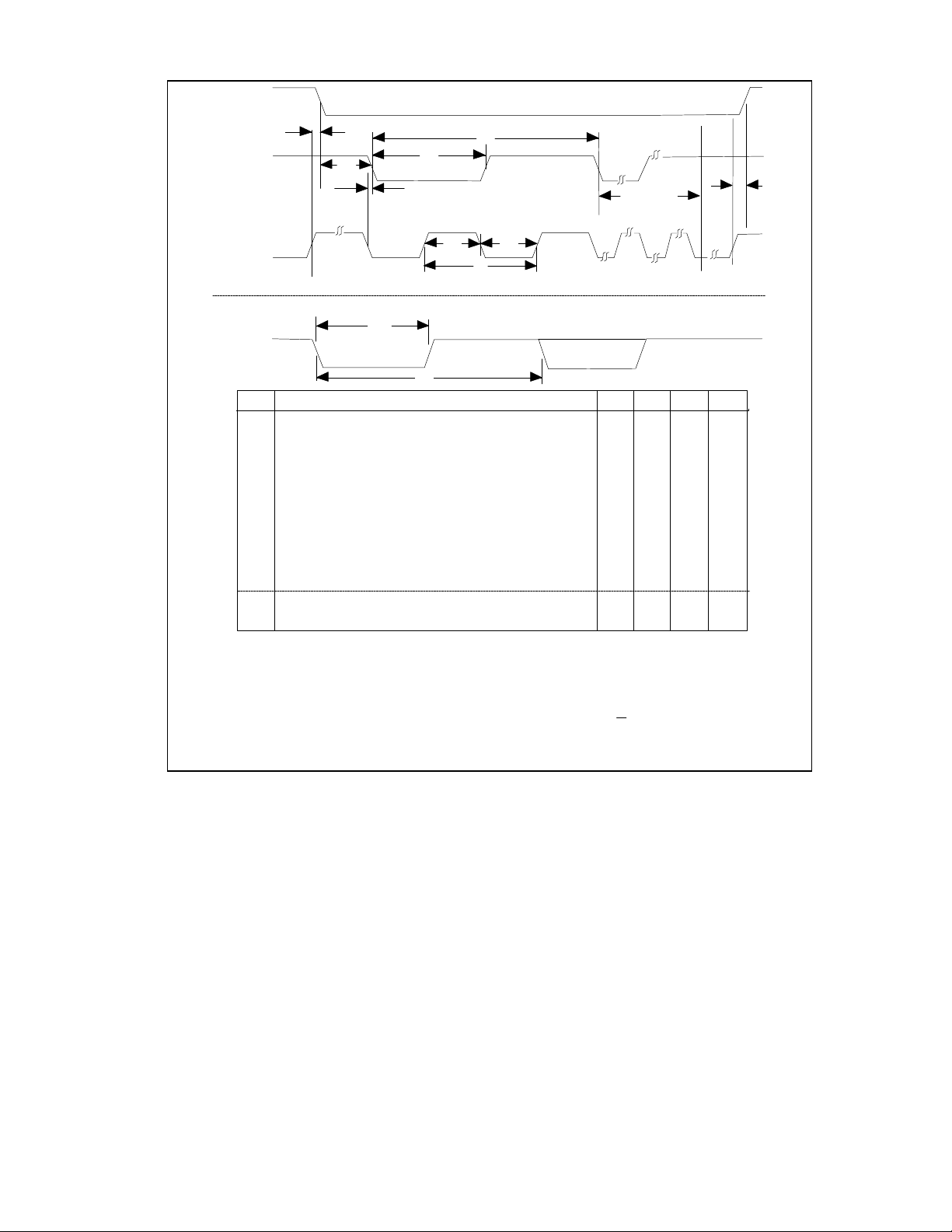
55
nTXEN
** t9: For clock frequencies other than 20 MHz, t9 = 14 x (clock period)+ 50 nsec.
nPULSE1
t1
t3
t9
t4
t2
LAST BIT
(400 nS BIT TIME)
t8
nPULSE2
(Internal Clk)
t10
RXIN
Parameter min typ max units
nPULSE2 High to nTXEN Low
t1
t2
nPULSE1 Pulse Width
t3
nPULSE1 Period
t4
nPULSE2 Low to nPULSE1 Low
t5
nPULSE2 High Time
t6
nPULSE2 Low Time
t7
nPULSE2 Period
t8
nPULSE2 High to nTXEN High
(First rising edge on nPULSE2 after Last Bit Time)
t9
nTXEN Low to first nPULSE1 Low**
t10
RXIN Pulse Width
t11
RXIN Period
* t5,t6 = 2 x (crystal period) for clock frequencies other than 20 MHz.
* t2,t7,t10 = 4 x (crystal period) for clock frequencies other than 20 MHz.
* t3,t11 = 8 x (crystal period) for clock frequencies other than 20 MHz.
This period applies to data of two consecutive one's.
t5 t6
t7
t11
0 50
200*
400*
-25
0
650 750
10
25
100*
100*
200*
50
200*
400*
nS
nS
nS
nS
nS
nS
nS
nS
nS
nS
nS
FIGURE 15 - BACKPLANE MODE TRANSMIT OR RECEIVE TIMING
(These signals are to and from the differential driver or the cable)
Page 56

56
XTAL1
nRESET IN
nINTR High to Next nINTR Low
nINTR
t1
t2
t3
Parameter
t1
t2 Input Clock Low Time
t3
t4 Input Clock Frequency
Input Clock High Time
Input Clock Period
FIGURE 16 - TTL INPUT TIMING ON XTAL1 PIN
t1
Parameter
t1
nRESET IN Pulse Width
t2
FIGURE 17 - RESET AND INTERRUPT TIMING
min
20
20
50
10
typ
max units
nS
nS
100
nS
20 MHz
t2
min
3.2
200
typ
max units
µS
nS
Page 57

57
right above it on a beveled edge.
2.
G
B
a
s
e
P
l
a
n
e
S
e
a
t
i
n
g
P
l
a
n
e
PIN NO.
E
1
J
F
B1
D3
A
B
D2
R
J
D1
D
J
C
A1
DIM 28L
A
A1
B
B1
C
D
D1
D2
D3
E
F
G
.160-.180
.090-.120
.013-.021
.026-.032
.020-.045
.485-.495
.450-.456
.390-.430
.300 REF
.050 BSC
.042-.056
.042-.048
J .000-.020
R
.025-.045
NOTES:
1.
All dimensions are in inches.
Circle indicating pin 1 can appear on a top surface as shown on the drawing or
FIGURE 18 - 28-PIN PLCC PACKAGE DIMENSIONS
Page 58

58
E1 E
Note: All dimensions are in inches.
Base
Plane
Seating
Plane
e
D
A2
A
A1
L
B1
S
e
DIM
A
A1
A2
B
B1
C
D
E
E1
e
eA
eB
L
S
B
24L
.090-.150
.020-.065
.145-.155
.016-.021
.060-.070
.010-.014
1.245-1.265
.590-.630
.530-.545
.100BSC
.600REF
.610-.670
.120-.140
.065-.085
A
e
B
C
FIGURE 18A - 24-PIN DIP PACKAGE DIMENSIONS
Page 59

59
COM20020 ERRATA SHEET
DATE
PAGE SECTION/FIGURE/ENTRY CORRECTION
5 Pin No. 18/DESCRIPTION See Italicized Text 5/29/96
8 Network Protocol See Italicized Text 5/29/96
9 Network Reconfiguration See Italicized Text 5/29/96
9 Extended Timeout Function See Italicized Text 5/29/96
10 Line Protocol See Italicized Text 5/29/96
12 Microcontroller Interface See Italicized Text 5/29/96
15 Backplane Configuration See Italicized Text 5/29/96
17 Programmable TXEN Polarity See Italicized Text 5/29/96
22 Data Register See Italicized Text 5/29/96
23 Status Register See Italicized Text 5/29/96
23 Address Pointer Registers See Italicized Text 5/29/96
24 Configuration Register See Italicized Text 5/29/96
29 Table 9 Bits 4,3 - See Italicized Text 5/29/96
30 Table 10 Bit 5 and Bits 3,2,1 - See Italicized
Text
35 Transmit Sequence See Italicized Text 5/29/96
40 Bus Determination See Italicized Text 5/29/96
42 Abnormal Results See Italicized Text 5/29/96
REVISED
5/29/96
Page 60

STANDARD MICROSYSTEMS CORP.
Circuit diagrams utilizing SMSC products are included as a means of illustrating
typical applications; consequently complete information sufficient for
construction purposes is not necessarily given. The information has been
carefully checked and is believed to be entirely reliable. However, no
responsibility is assumed for inaccuracies. Furthermore, such information does
not convey to the purchaser of the semiconductor devices described any
licenses under the patent rights of SMSC or others. SMSC reserves the right to
make changes at any time in order to improve design and supply the best
product possible. SMSC products are not designed, intended, authorized or
warranted for use in any life support or other application where product failure
could cause or contribute to personal injury or severe property damage. Any
and all such uses without prior written approval of an Officer of SMSC and
further testing and/or modification will be fully at the risk of the customer.
COM20020 Rev. 5/29/96
 Loading...