

SMOS SED1520FOA, SED1521FAA, SED1521FOA, SED1520FAA Datasheet

S-MOS Systems, Inc. • 150 River Oaks Parkway • San Jose, CA 95134 • Tel: (408) 922-0200 • Fax: (408) 922-0238
371-1.0
1
SED1520/21
DOT MATRIX LCD DRIVER
S-MOS Systems, Inc.
October, 1996
Version 1.0 (Preliminary)

–
S-MOS Systems, Inc. • 150 River Oaks Parkway • San Jose, CA 95134 • Tel: (408) 922-0200 • Fax: (408) 922-0238
371-1.0
2
THIS PAGE INTENTIONALLY BLANK

S-MOS Systems, Inc. • 150 River Oaks Parkway • San Jose, CA 95134 • Tel: (408) 922-0200 • Fax: (408) 922-0238
371-1.0
3
Table of Contents
1.0 GENERAL DESCRIPTION . . . . . . . . . . . . . . . . . . . . . . . . . . . . . . . . . . . . . . . . . . . . . . . . . . . . . . . . . . . . . . . 5
1.1 Description . . . . . . . . . . . . . . . . . . . . . . . . . . . . . . . . . . . . . . . . . . . . . . . . . . . . . . . . . . . . . . . . . . . . . . 5
1.2 Features . . . . . . . . . . . . . . . . . . . . . . . . . . . . . . . . . . . . . . . . . . . . . . . . . . . . . . . . . . . . . . . . . . . . . . . . 5
1.3 SED1520 Family Specifications . . . . . . . . . . . . . . . . . . . . . . . . . . . . . . . . . . . . . . . . . . . . . . . . . . . . . . 6
1.4 Model Classification . . . . . . . . . . . . . . . . . . . . . . . . . . . . . . . . . . . . . . . . . . . . . . . . . . . . . . . . . . . . . . . 6
2.0 BLOCK DIAGRAMS . . . . . . . . . . . . . . . . . . . . . . . . . . . . . . . . . . . . . . . . . . . . . . . . . . . . . . . . . . . . . . . . . . . . 7
2.1 System Block Diagram . . . . . . . . . . . . . . . . . . . . . . . . . . . . . . . . . . . . . . . . . . . . . . . . . . . . . . . . . . . . . 7
2.2 Block Diagram . . . . . . . . . . . . . . . . . . . . . . . . . . . . . . . . . . . . . . . . . . . . . . . . . . . . . . . . . . . . . . . . . . . 8
2.3 Description of Circuit Blocks . . . . . . . . . . . . . . . . . . . . . . . . . . . . . . . . . . . . . . . . . . . . . . . . . . . . . . . . . 9
2.3.1 MPU Interface . . . . . . . . . . . . . . . . . . . . . . . . . . . . . . . . . . . . . . . . . . . . . . . . . . . . . . . . 9
2.3.2 Busy Flag . . . . . . . . . . . . . . . . . . . . . . . . . . . . . . . . . . . . . . . . . . . . . . . . . . . . . . . . . . . 11
2.3.3 Display Start Line Register . . . . . . . . . . . . . . . . . . . . . . . . . . . . . . . . . . . . . . . . . . . . . 11
2.3.4 Column Address Counter . . . . . . . . . . . . . . . . . . . . . . . . . . . . . . . . . . . . . . . . . . . . . . 11
2.3.5 Page Register . . . . . . . . . . . . . . . . . . . . . . . . . . . . . . . . . . . . . . . . . . . . . . . . . . . . . . . 11
2.3.6 Display Data RAM . . . . . . . . . . . . . . . . . . . . . . . . . . . . . . . . . . . . . . . . . . . . . . . . . . . . 11
2.3.7 Common Timing Generator . . . . . . . . . . . . . . . . . . . . . . . . . . . . . . . . . . . . . . . . . . . . . 12
2.3.8 Display Data Latch Circuit . . . . . . . . . . . . . . . . . . . . . . . . . . . . . . . . . . . . . . . . . . . . . . 12
2.3.9 LCD Driver Circuit . . . . . . . . . . . . . . . . . . . . . . . . . . . . . . . . . . . . . . . . . . . . . . . . . . . . 14
2.3.10 Display Timing Generator . . . . . . . . . . . . . . . . . . . . . . . . . . . . . . . . . . . . . . . . . . . . . . 14
2.3.11 Oscillation Circuit . . . . . . . . . . . . . . . . . . . . . . . . . . . . . . . . . . . . . . . . . . . . . . . . . . . . . 14
2.3.12 Reset Circuit . . . . . . . . . . . . . . . . . . . . . . . . . . . . . . . . . . . . . . . . . . . . . . . . . . . . . . . . 16
3.0 PIN CONFIGURATION . . . . . . . . . . . . . . . . . . . . . . . . . . . . . . . . . . . . . . . . . . . . . . . . . . . . . . . . . . . . . . . . . 19
3.1 Pin Configuration . . . . . . . . . . . . . . . . . . . . . . . . . . . . . . . . . . . . . . . . . . . . . . . . . . . . . . . . . . . . . . . . 19
3.2 Pin Description . . . . . . . . . . . . . . . . . . . . . . . . . . . . . . . . . . . . . . . . . . . . . . . . . . . . . . . . . . . . . . . . . . 20
3.2.1 Power Signals . . . . . . . . . . . . . . . . . . . . . . . . . . . . . . . . . . . . . . . . . . . . . . . . . . . . . . . 20
3.2.2 System Bus Interface Signals . . . . . . . . . . . . . . . . . . . . . . . . . . . . . . . . . . . . . . . . . . . 20
3.2.3 LCD Drive Circuit Signals . . . . . . . . . . . . . . . . . . . . . . . . . . . . . . . . . . . . . . . . . . . . . . 21
4.0 COMMANDS . . . . . . . . . . . . . . . . . . . . . . . . . . . . . . . . . . . . . . . . . . . . . . . . . . . . . . . . . . . . . . . . . . . . . . . . . 23
4.1 Display ON/OFF . . . . . . . . . . . . . . . . . . . . . . . . . . . . . . . . . . . . . . . . . . . . . . . . . . . . . . . . . . . . . . . . . 23
4.2 Display Start Line . . . . . . . . . . . . . . . . . . . . . . . . . . . . . . . . . . . . . . . . . . . . . . . . . . . . . . . . . . . . . . . . 23
4.3 Set Page Address . . . . . . . . . . . . . . . . . . . . . . . . . . . . . . . . . . . . . . . . . . . . . . . . . . . . . . . . . . . . . . . 24
4.4 Column Address . . . . . . . . . . . . . . . . . . . . . . . . . . . . . . . . . . . . . . . . . . . . . . . . . . . . . . . . . . . . . . . . . 24
4.5 Read Status. . . . . . . . . . . . . . . . . . . . . . . . . . . . . . . . . . . . . . . . . . . . . . . . . . . . . . . . . . . . . . . . . . . . . 25
4.6 Write Display Data . . . . . . . . . . . . . . . . . . . . . . . . . . . . . . . . . . . . . . . . . . . . . . . . . . . . . . . . . . . . . . . 25
4.7 Read Display Data . . . . . . . . . . . . . . . . . . . . . . . . . . . . . . . . . . . . . . . . . . . . . . . . . . . . . . . . . . . . . . . 26
4.8 Select ADC . . . . . . . . . . . . . . . . . . . . . . . . . . . . . . . . . . . . . . . . . . . . . . . . . . . . . . . . . . . . . . . . . . . . . 26
4.9 Static Drive ON/OFF . . . . . . . . . . . . . . . . . . . . . . . . . . . . . . . . . . . . . . . . . . . . . . . . . . . . . . . . . . . . . . 26
4.10 Select Duty . . . . . . . . . . . . . . . . . . . . . . . . . . . . . . . . . . . . . . . . . . . . . . . . . . . . . . . . . . . . . . . . . . . . . 27

Table of Contents
S-MOS Systems, Inc. • 150 River Oaks Parkway • San Jose, CA 95134 • Tel: (408) 922-0200 • Fax: (408) 922-0238
371-1.0
4
4.11 Read Modify Write . . . . . . . . . . . . . . . . . . . . . . . . . . . . . . . . . . . . . . . . . . . . . . . . . . . . . . . . . . . . . . . 27
4.11.1 Cursor Blinking Sequence . . . . . . . . . . . . . . . . . . . . . . . . . . . . . . . . . . . . . . . . . . . . . 28
4.12 End . . . . . . . . . . . . . . . . . . . . . . . . . . . . . . . . . . . . . . . . . . . . . . . . . . . . . . . . . . . . . . . . . . . . . . . . . . 28
4.12.1 End Timing . . . . . . . . . . . . . . . . . . . . . . . . . . . . . . . . . . . . . . . . . . . . . . . . . . . . . . . . . 28
4.13 Reset . . . . . . . . . . . . . . . . . . . . . . . . . . . . . . . . . . . . . . . . . . . . . . . . . . . . . . . . . . . . . . . . . . . . . . . . . 29
4.14 Save Power (Combined Command) . . . . . . . . . . . . . . . . . . . . . . . . . . . . . . . . . . . . . . . . . . . . . . . . . 29
4.14.1 External Resistor Division Circuit . . . . . . . . . . . . . . . . . . . . . . . . . . . . . . . . . . . . . . . . 29
5.0 ELECTRICAL CHARACTERISTICS . . . . . . . . . . . . . . . . . . . . . . . . . . . . . . . . . . . . . . . . . . . . . . . . . . . . . . 31
5.1 Absolute Maximum Ratings . . . . . . . . . . . . . . . . . . . . . . . . . . . . . . . . . . . . . . . . . . . . . . . . . . . . . . . . 31
5.2 DC Characteristics . . . . . . . . . . . . . . . . . . . . . . . . . . . . . . . . . . . . . . . . . . . . . . . . . . . . . . . . . . . . . . . 32
5.3 Timing Characteristics . . . . . . . . . . . . . . . . . . . . . . . . . . . . . . . . . . . . . . . . . . . . . . . . . . . . . . . . . . . . 35
5.3.1 System Bus Read/Write I (80 Family MPU) . . . . . . . . . . . . . . . . . . . . . . . . . . . . . . . . 35
5.3.2 System Bus Read/Write II (68 Family MPU) . . . . . . . . . . . . . . . . . . . . . . . . . . . . . . . . 36
5.3.3 Display Control Timing. . . . . . . . . . . . . . . . . . . . . . . . . . . . . . . . . . . . . . . . . . . . . . . . . 37
6.0 MPU INTERFACE . . . . . . . . . . . . . . . . . . . . . . . . . . . . . . . . . . . . . . . . . . . . . . . . . . . . . . . . . . . . . . . . . . . . . 39
6.1 80 Family MPU . . . . . . . . . . . . . . . . . . . . . . . . . . . . . . . . . . . . . . . . . . . . . . . . . . . . . . . . . . . . . . . . . 39
6.2 68 Family MPU . . . . . . . . . . . . . . . . . . . . . . . . . . . . . . . . . . . . . . . . . . . . . . . . . . . . . . . . . . . . . . . . . 40
7.0 LCD DRIVER INTERCONNECTIONS . . . . . . . . . . . . . . . . . . . . . . . . . . . . . . . . . . . . . . . . . . . . . . . . . . . . . 41
7.1 SED1520FOA - SED1520FOA . . . . . . . . . . . . . . . . . . . . . . . . . . . . . . . . . . . . . . . . . . . . . . . . . . . . . 41
7.2 SED1520FAA - SED1520FAA . . . . . . . . . . . . . . . . . . . . . . . . . . . . . . . . . . . . . . . . . . . . . . . . . . . . . . 41
7.3 SED1520FOA - SED1521FOA *1 . . . . . . . . . . . . . . . . . . . . . . . . . . . . . . . . . . . . . . . . . . . . . . . . . . 41
7.4 SED1520FAA - SED1521FAA . . . . . . . . . . . . . . . . . . . . . . . . . . . . . . . . . . . . . . . . . . . . . . . . . . . . . . 42
7.5 HD44103CH - SED1521FAA . . . . . . . . . . . . . . . . . . . . . . . . . . . . . . . . . . . . . . . . . . . . . . . . . . . . . . . 42
8.0 TYPICAL CONNECTIONS WITH LCD PANEL . . . . . . . . . . . . . . . . . . . . . . . . . . . . . . . . . . . . . . . . . . . . . . 43
8.1 Duty 1/16, 10 characters x 2 lines . . . . . . . . . . . . . . . . . . . . . . . . . . . . . . . . . . . . . . . . . . . . . . . . . . . 43
8.2 Duty 1/16, 23 characters x 2 lines . . . . . . . . . . . . . . . . . . . . . . . . . . . . . . . . . . . . . . . . . . . . . . . . . . . 43
8.3 Duty 1/32, 33 characters x 4 lines . . . . . . . . . . . . . . . . . . . . . . . . . . . . . . . . . . . . . . . . . . . . . . . . . . . 44
8.4 Duty 1/32, 20 kanji characters x 2 lines . . . . . . . . . . . . . . . . . . . . . . . . . . . . . . . . . . . . . . . . . . . . . . . 44
8.5 Duty 1/32, 2–screen display, 20 kanji characters x 4 lines. . . . . . . . . . . . . . . . . . . . . . . . . . . . . . . . . 45
9.0 PACKAGE DIMENSIONS . . . . . . . . . . . . . . . . . . . . . . . . . . . . . . . . . . . . . . . . . . . . . . . . . . . . . . . . . . . . . . . 47
9.1 Plastic QFP 5-100 Pin . . . . . . . . . . . . . . . . . . . . . . . . . . . . . . . . . . . . . . . . . . . . . . . . . . . . . . . . . . . . 47
10.0 PAD LAYOUT . . . . . . . . . . . . . . . . . . . . . . . . . . . . . . . . . . . . . . . . . . . . . . . . . . . . . . . . . . . . . . . . . . . . . . . . 49
10.1 Pad Layout (SED1520D/SED1521D) . . . . . . . . . . . . . . . . . . . . . . . . . . . . . . . . . . . . . . . . . . . . . . . . 49
10.1.1 Al Pad . . . . . . . . . . . . . . . . . . . . . . . . . . . . . . . . . . . . . . . . . . . . . . . . . . . . . . . . . . . . . 50
10.1.2 Au Bump Pad . . . . . . . . . . . . . . . . . . . . . . . . . . . . . . . . . . . . . . . . . . . . . . . . . . . . . . . 50
10.2 Pad Coordinates (SED1520DAB) . . . . . . . . . . . . . . . . . . . . . . . . . . . . . . . . . . . . . . . . . . . . . . . . . . . 51

S-MOS Systems, Inc. • 150 River Oaks Parkway • San Jose, CA 95134 • Tel: (408) 922-0200 • Fax: (408) 922-0238
371-1.0
5
1.0 General Description 1.0 – 1.2
1.0 GENERAL DESCRIPTION
1.1 DESCRIPTION
The SED1520 is a dot matrix LCD driver LSI intended for display of characters and graphics. The
bit-addressable display data, which is sent from a microcomputer, is stored in a built-in display data
RAM and generates the LCD drive signal.
The SED1520 incorporates innovative circuit design strategies to assure very low current dissipation and a wide range of operating voltages. With these features, the SED1520 permits the user to
implement high-performance handy systems operating from a miniature battery.
In order for the user to adaptively configure his system, the SED1520 family offers two application
forms. One form allows an LCD display of 12 characters
×
2 lines with an indicator with a single
chip. The other is dedicated to driving a total of 80 segments, enabling a medium-size display to
be achieved by using a minimum number of drivers.
1.2 FEATURES
•
Low-power CMOS technology
•
Fast CPU 8-bit data interface (80xx, 68xx)
•
Segment output . . . . . . . . . . 61 outputs
•
Common output . . . . . . . . . . 16 outputs
•
Duty cycle . . SED1520 . . . 1/16 to 1/32
SED1521 . . . 1/8 to 1/32
•
Built-in display data RAM. . . 2560 bits
•
Rich display command setting
•
On-chip CR oscillation circuit
•
Recommended expansion segment driver: 80 bit
•
Master/slave operation is supported
•
Low power consumption . . . 30 µ W
•
LCD voltage. . . . . . . . . . . . . 3.5 to 13V
•
Single power supply. . . . . . . 2.4 to 7.0V
•
Package. . . . . . . . . . . . . . . . QFP5-100 pin (F
OA
, F
AA
)
QFP15-100 pin (F
OC
, F
AC
)
Al pad (D
OA
, D
AA
)
Au bump (D
OB
, D
AB
)
TAB (T
OA
)
1.3 – 1.4 1.0 General Description
S-MOS Systems, Inc. • 150 River Oaks Parkway • San Jose, CA 95134 • Tel: (408) 922-0200 • Fax: (408) 922-0238
371-1.0
6
1.3 SED1520 FAMILY SPECIFICATIONS
1.4 MODEL CLASSIFICATION
Product Name
Clock Frequency
Applicable Driver
No. of SEG
Drivers
No. of COM
Drivers
On Chip External
SED1520F
OA
18kHz 18kHz
SED1520F
OA
,
SED1521F
OA
61 16
SED1521F
OA
— 18kHz 80 0
SED1520F
AA
— 2kHz SED1520F
AA
,
SED1521F
AA
,
HD44103CH
61 16
SED1521F
AA
— 2kHz 80 0
Model Name
Operating Clock
Connectable Drivers
SEG
Driver
COM
Driver
Internal
oscillator
External
clock
SED1520F
O*
18KHz 18KHz SED1520F
O*
, SED1521F
O*
61 ports 16 ports
SED1520F
A*
— 2KHz SED1520F
A*
, SED1521F
A*
61 ports 16 ports
S-MOS Systems, Inc. • 150 River Oaks Parkway • San Jose, CA 95134 • Tel: (408) 922-0200 • Fax: (408) 922-0238
371-1.0
7
2.0 Block Diagrams 2.0 – 2.1
2.0 BLOCK DIAGRAMS
2.1 SYSTEM BLOCK DIAGRAM
SEG0~SEG60
28 CHAR × 2 LINES
CPU (68xx, 80xx)
SED1521SED1520
SEG0~SEG79
DATA
CONTROL
FR
Ck
M/S M/S
GND
V
DD
COM0~COM15
2.2 – 2.2 2.0 Block Diagrams
S-MOS Systems, Inc. • 150 River Oaks Parkway • San Jose, CA 95134 • Tel: (408) 922-0200 • Fax: (408) 922-0238
371-1.0
8
2.2 BLOCK DIAGRAM
LINE ADDRESS DECODER
DISPLAY DATA RAM
2560 BITS
I/O BUFFER
INTERNAL BUS
LOW ADDRESS
REGISTER
BUS
HOLDER
LINE COUNTER
DISPLAY
TIMING
GENERATOR
DISPLAY START LINE REGISTER
FR
COMMAND
DECODER
COLUMN ADDRESS REGISTER
STATUS
MPU INTERFACE
COLUMN ADDRESS COUNTER
COLUMN ADDRESS DECODER
DISPLAY DATA LATCH CIRCUIT
LCD DRIVER CIRCUIT
COMMON
COUNTER
CL
(OSC2)
D
0
D
A
E , R/W
(OSC1)
RES
(RD)(WR)
0
, CS
7
∼
∼
V
DD
V
SS
V , V , M/S
1
V , V , V
235
(SG SG )
77 79
∼(SG SG )
61 76
∼ SG SG
060
∼CM CM
015
4
S-MOS Systems, Inc. • 150 River Oaks Parkway • San Jose, CA 95134 • Tel: (408) 922-0200 • Fax: (408) 922-0238
371-1.0
9
2.0 Block Diagrams 2.3 – 2.3.1.3
2.3 DESCRIPTION OF CIRCUIT BLOCKS
2.3.1 MPU Interface
2.3.1.1 Selection of Interface Type
The SED1520 Series uses 8 bits of bi-directional data bus (D0–D7) to transfer data. The reset pin
is capable of selecting MPU interface; setting the polarity of RES
to either “H” or “L” can provide
direct interface of the SED1520 with a 68 or 80 family MPU (see Table 1 below).
With CS
at high level, the SED1520 is independent from the MPU bus and stays in standby mode.
In this mode, however, the reset signal is input independently of the internal status.
Table 1
2.3.1.2 Identification of Data Bus Signals
The SED1520 uses a combination of A0, E, R/W, (RD, WR) to identify a data bus signal.
Table 2
2.3.1.3 Access to Display Data RAM and Internal Register
In order to make matching of operating frequencies between the MPU and the display data RAM
or internal register, the SED1520 performs a sort of LSI–LSI pipelining via the bus holder attached
to the internal data bus.
Consider the case where the MPU reads the content of the display data RAM. In the first data read
cycle (dummy), the data is stored on the bus holder. In the next data read cycle, the data is read
from the bus holder to the system bus.
Also, consider the case where the MPU writes data to the display data RAM. In the first data write
cycle, the data is held on the bus holder. The data is written to the display data RAM before the
next data write cycle begins.
Polarity of RES
Type A0 E R/W CS D0–D7
“L” active 68 MPU
↑↑↑↑ ↑
“H” active 80 MPU
↑
RD WR
↑↑
Common 68 MPU 80 MPU
Function
A0 R/W RD
WR
1101Read display data
1010Write display data
0101Read status
0010Write to internal register (command)
2.3.1.4 – 2.3.1.5 2.0 Block Diagrams
S-MOS Systems, Inc. • 150 River Oaks Parkway • San Jose, CA 95134 • Tel: (408) 922-0200 • Fax: (408) 922-0238
371-1.0
10
Therefore, MPU’s access to the SED1520 is affected not by display data RAM access time (t
ACC
,
t
DS
) but by cycle time (t
CYC
). This leads to faster transfer of data to and from the MPU. If the cycle
time requirement is not met, the MPU has only to execute the NOP instruction and this is apparently equivalent to execution of a waiting operation. However, there is a restriction on the read
sequence of the display data RAM; when an address is set, its data is output not to the first read
instruction (immediately following the address setting operation) but to the second read instruction.
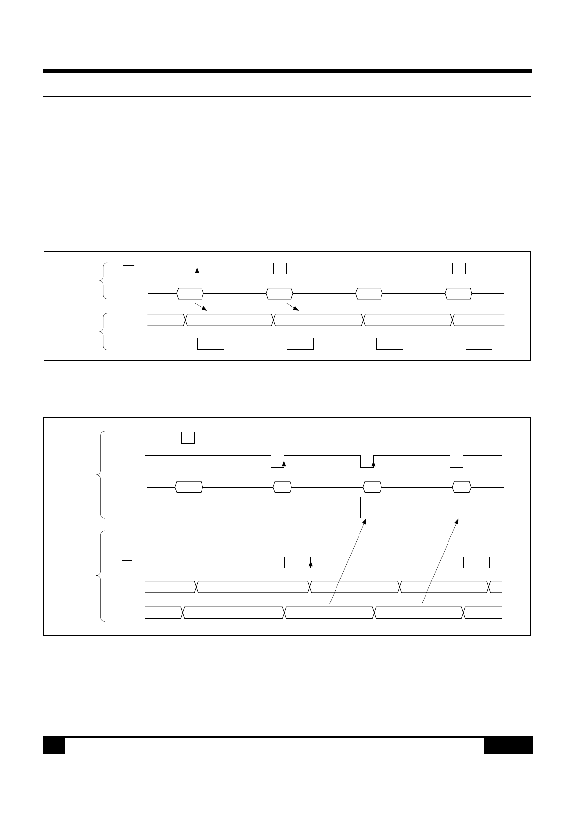
Thus, one dummy read cycle is necessary after an address set or write cycle. This relation is
shown in Figures 2.3.1.4 and 2.3.1.5.
2.3.1.4 Write Timing Diagram
2.3.1.5 Read Timing Diagram
WR
DATA
MPU
Bus
Holder
WR
N N + 1 N + 2 N + 3
N + 2N + 1N N + 3
Internal
Timing
WR
DATA
MPU
Bus
Holder
Column
Address
WR
RD
RD
N
Address Set
at N
Dummy Read Data Read
at N
Data Read
at N+1
N n n+1
n + 1nN n + 2
N + 2N + 1N
Internal
Timing

S-MOS Systems, Inc. • 150 River Oaks Parkway • San Jose, CA 95134 • Tel: (408) 922-0200 • Fax: (408) 922-0238
371-1.0
11
2.0 Block Diagrams 2.3.2 – 2.3.6
2.3.2 Busy Flag
Busy flag being “1” means that the SED1520 is performing its internal operation and any instruction
other than Read Status is disabled. The busy flag is output to pin D7 by a Read Status instruction.
As long as the cycle time (t
CYC
) requirement is met, the flag need not be checked before each com-
mand and this dramatically improves the MPU performance.
2.3.3 Display Start Line Register
This register is a pointer which determines the start line corresponding to COM0 (normally, the uppermost line of display) for display of data in the display data RAM. It is used for scrolling the display or changing the page from one to another. Executing the Set Display Start Line command
sets 5 bits of display start address in this register. Its content is preset in the line counter at each
timing the FR signal changes. The line counter is incremented synchronously to a CL input, thus
generating a line address for sequential reading of 80 bits of data from the display data RAM to the
LCD driver circuit.
2.3.4 Column Address Counter
The column address counter is a 7–bit presettable counter which gives column addresses of the
display data RAM as shown in Fig. 2.3.8.1. When a Read/Write Display Data command comes in,
the counter is incremented by 1. For any nonexisting address over 50H, the counter is locked and
not incremented.
The column address counter is independent from the page register.
2.3.5 Page Register
This register gives a page address of the display data RAM as shown in Fig. 2.3.8.1. The Set Page
Address command permits the MPU to access a new page of the display data RAM.
2.3.6 Display Data RAM
Dot data for display is stored in this RAM. Since the MPU and LCD driver circuit operate independently of each other, data can be changed asynchronously without adverse effect on the display.
One bit of the display data RAM is assigned to one bit of LCD:
LCD on = “1”
LCD off = “0”
The ADC command inverts the assignment relationship between a display data RAM column address and a segment output (see Fig. 2.3.8.1).
2.3.7 – 2.3.8 2.0 Block Diagrams
S-MOS Systems, Inc. • 150 River Oaks Parkway • San Jose, CA 95134 • Tel: (408) 922-0200 • Fax: (408) 922-0238
371-1.012
2.3.7 Common Timing Generator
This circuit generates common timing and frame (FR) signals from the basic clock (CL). The Select Duty command selects a duty of 1/16 or 1/32. The 1/32 duty is achieved by a two-chip (master
and slave) configuration (common multi-chip system).
2.3.7.1 Common Timing Diagram
2.3.8 Display Data Latch Circuit
The display data latch circuit temporarily stores the data which will be output from the display
data RAM to the LCD driver circuit at one-common intervals. The display ON/OFF and Static
Driver ON/OFF commands control the latched data so that the data in the display data RAM
remains unchanged.
0 1 21415 01 15
16 17 30 31 16 17 31
FR
(Master
Output)
Master
Common
Slave
Common
S-MOS Systems, Inc. • 150 River Oaks Parkway • San Jose, CA 95134 • Tel: (408) 922-0200 • Fax: (408) 922-0238
371-1.0 13
2.0 Block Diagrams 2.3.8.1 – 2.3.8.1
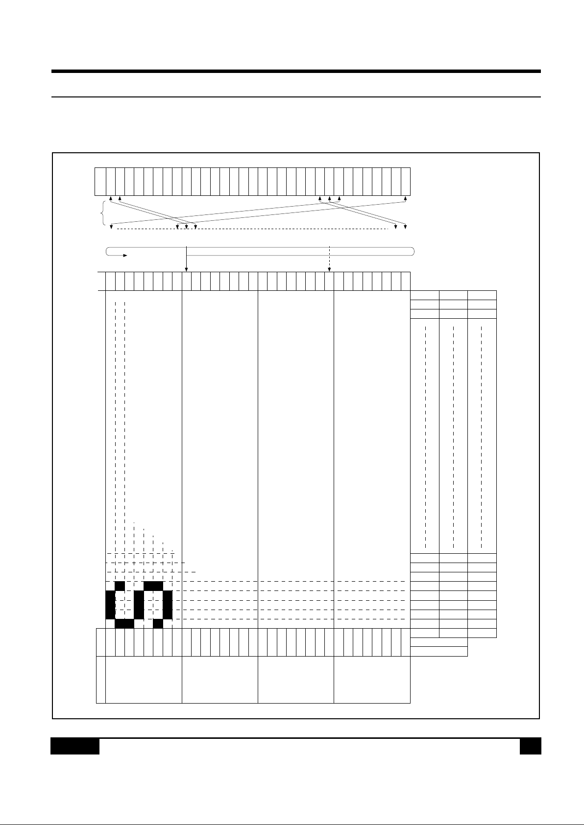
2.3.8.1 Relationship between Display Data RAM Locations and Addresses (Display Start
Line: 08)
Page Address
D1,D2=0,0
0,1
1,0
1,1
COM 0
123456789
101112131415161718192021222324252627282930
31
DATA
D
0
D1D2D3D4D5D6D7D0D1D2D3D4D5D6D7D0D1D2D3D4D5D6D7D0D1D2D3D4D5D6D7
Page 0
Page 1
Page 2
Page 3
(In this example,
the display start
line is set at
address 08.)
Start
1/16
Line
address
Associated
Line (ex.)
Assignment
Common
Output
00H
010203040506070809
0A
0B
0C
0D
0E
0F
101112131415161718
19
1A
1B
1C
1D
1E
1F
Column Address
ADC
Display Area
SEG Pin
SEG 0
1
2
3
4
5
6
7
D
0=“I”
4F
H
4E
4D
4C
4B
4A
49
48
D
0=“O”
00
H
01
02
03
04
05
06
07
77
78
79
02
01
00
4D
4E
4F

2.3.9 – 2.3.11 2.0 Block Diagrams
S-MOS Systems, Inc. • 150 River Oaks Parkway • San Jose, CA 95134 • Tel: (408) 922-0200 • Fax: (408) 922-0238
371-1.014
2.3.9 LCD Driver Circuit
This circuit generates 80 sets of multiplexer that generate quartet levels for LCD driving. Display
data in the display data latch, common timing generator output and FR signal are combined to output an LCD driving waveform.
2.3.10 Display Timing Generator
This circuit generates an internal display timing signal from the basic clock (CL) and frame signal (FR).
The frame signal FR makes the LCD driver circuit generate a dual frame AC driving waveform
(type B) to drive LCD, while making both the line counter and common timing generator synchronized to the FR signal output LSI (dedicated common driver or the SED1520 master LSI). To
achieve these functions, the FR signal must be a clock with a duty of 50% which is synchronized
to the frame period.
The clock CL is a clock used to operate the line counter. For a system in which both the SED1520
and SED1521F coexist, they should be of LSI types having the same clock frequency to be applied
to pin CL.
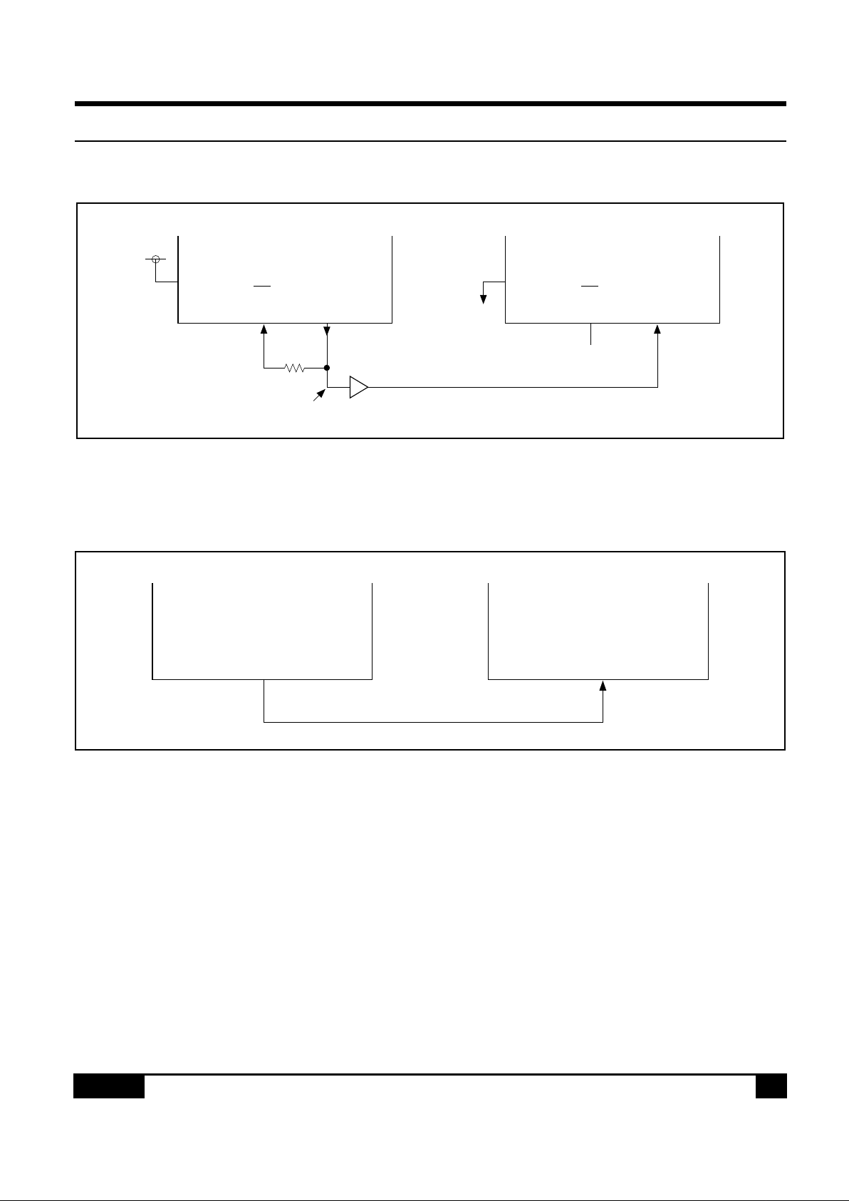
2.3.11 Oscillation Circuit
This circuit is a low-power CR oscillator which uses an oscillation resistor Rf alone to adjust the
oscillation frequency. It generates display timing signals. The SED1520 is available in two LSI
types if classified by oscillation: one LSI type contains an oscillation circuit and the other uses an
externally provided clock.
The oscillation resistor Rf is connected as shown below. Where an LSI containing an oscillation
circuit is operated with an external clock, it is necessary to input the clock with the same phase as
OSC2 of the master LSI to OSC2 of the slave LSI.
S-MOS Systems, Inc. • 150 River Oaks Parkway • San Jose, CA 95134 • Tel: (408) 922-0200 • Fax: (408) 922-0238
371-1.0 15
2.0 Block Diagrams 2.3.11.1 – 2.3.11.2
2.3.11.1 LSI Containing Oscillator
* As the parasitic capacitance in this portion increases, the oscillation frequency will shift to a lower level. The Rf must
have a smaller value than the specification.
* For a system having two or more slave LSIs, a CMOS buffer is necessary.
2.3.11.2 LSI Operating with External Clock
Master LSI
(CS)
OSC1
M/S
VDD
VSS
(CL)
OSC2
R
f
*1
*2
( )
Slave LSI
(CS)
OSC1
Open
M/S
(CL)
OSC2
Y-Driver
CL2
SED1521F
AA
CL

2.3.12 – 2.3.12 2.0 Block Diagrams
S-MOS Systems, Inc. • 150 River Oaks Parkway • San Jose, CA 95134 • Tel: (408) 922-0200 • Fax: (408) 922-0238
371-1.016
2.3.12 Reset Circuit
This circuit senses the leading edge or trailing edge of RES and initializes the system when its
power is switched on.
Initialization:
(a) Display off
(b) Display start line register: First line
(c) Static drive off
(d) Column address counter: Address 0
(e) Page address register: Page 0
(f) Select duty: 1/32
(g) Select ADC: Forward (ADC command D0 = “0”, ADC status flag = “1”)
(h) Read modify write off
The input at pin RES
is level-sensed to select an MPU interface mode as shown in Table 1. For
interfacing with an 80 family MPU, an “H” active reset signal is input to pin RES
. For interfacing
with a 68 family MPU, an “L” active reset signal is input to the pin. (See Fig. 7.)?????
As exemplified in section 6 “MPU Interface”, pin RES
is connected to the MPU reset pin. Thus the
SED1520 and the MPU are initialized at the same time. If system is initialized by pin RES
at power-
on, it may no longer be reset.
The Reset command causes initialization (b), (d) and (e).
 Loading...