

SMOS SED1330FBA, SED1330FBB, SED1335F0B, SED1335FOA, SED1336F0A Datasheet

S-MOS Systems, Inc. • 2460 North First Street • San Jose, CA 95131 • Tel: (408) 922-0200 • Fax: (408) 922-0238
268-0.4 1
SED1330F/1335F/1336F
LCD Controller ICs
Technical Manual
S-MOS Systems, Inc.
September, 1995
Version 0.4

S-MOS Systems, Inc. • 2460 North First Street • San Jose, CA 95131 • Tel: (408) 922-0200 • Fax: (408) 922-0238
2 268-0.4
THIS PAGE INTENTIONALLY BLANK

S-MOS Systems, Inc. • 2460 North First Street • San Jose, CA 95131 • Tel: (408) 922-0200 • Fax: (408) 922-0238
268-0.4 3
Table of Contents SED1330F/1335F/1336F
CONTENTS
1.0 Overview .............................................................................................................9
1.1 Description .................................................................................................................................. 11
1.2 Features ...................................................................................................................................... 11
1.3 Block Diagram ............................................................................................................................. 12
1.4 Pinouts ........................................................................................................................................14
1.4.1 SED1330FBA, 1335FBB and SED1336F0A Pinouts ............................................. 14
1.4.2 SED1330FBA and SED1335F0A Pinouts .............................................................. 14
1.5 Package Dimensions................................................................................................................... 15
2.0 Pin Description.................................................................................................17
2.1 SED1330FBA/BB Pin Summary.................................................................................................. 18
2.2 SED1330F/1335F0A/0B Pin Summary .......................................................................................19
2.3 SED1336F0A Pin Summary........................................................................................................ 20
2.4 Pin Functions...............................................................................................................................21
2.4.1 Power Supply..........................................................................................................21
2.4.2 Oscillator................................................................................................................. 21
2.4.3 Microprocessor Interface ........................................................................................21
2.4.4 Display Memory Control ......................................................................................... 23
2.4.5 LCD Drive Signals .................................................................................................. 23
3.0 Command Description.....................................................................................25
3.1 The Command Set ......................................................................................................................27
3.2 System Control Commands ........................................................................................................ 28
3.2.1 SYSTEM SET......................................................................................................... 28
3.2.1.1 C ........................................................................................................ 29
3.2.1.2 M0 ...................................................................................................... 29
3.2.1.3 M1 ...................................................................................................... 29
3.2.1.4 M2 ...................................................................................................... 29
3.2.1.5 W/S .................................................................................................... 29
3.2.1.6 IV........................................................................................................ 32
3.2.1.7 T/L...................................................................................................... 32
3.2.1.8 DR...................................................................................................... 32
3.2.1.9 FX ...................................................................................................... 32
3.2.1.10 WF ...................................................................................................33
3.2.1.11 FY..................................................................................................... 33
3.2.1.12 C/R....................................................................................................34
3.2.1.13 TC/R.................................................................................................34
3.2.1.14 L/F....................................................................................................35
3.2.1.15 AP ....................................................................................................35
3.2.2 SLEEP IN................................................................................................................36

S-MOS Systems, Inc. • 2460 North First Street • San Jose, CA 95131 • Tel: (408) 922-0200 • Fax: (408) 922-0238
4 268-0.4
SED1330F/1335F/1336F Table of Contents
3.3 Display Control Commands......................................................................................................... 36
3.3.1 DISP ON/OFF......................................................................................................... 36
3.3.1.1 D ........................................................................................................ 37
3.3.1.2 FC ...................................................................................................... 37
3.3.1.3 FP ...................................................................................................... 37
3.3.2 SCROLL ................................................................................................................. 37
3.3.2.1 C ........................................................................................................ 37
3.3.2.2 SL1, SL2 ............................................................................................ 38
3.3.3 CSRFORM..............................................................................................................42
3.3.3.1 CRX ...................................................................................................42
3.3.3.2 CRY .................................................................................................... 42
3.3.3.3 CM ..................................................................................................... 43
3.3.4 CSRDIR.................................................................................................................. 43
3.3.5 OVLAY....................................................................................................................43
3.3.5.1 MX0, MX1 .......................................................................................... 43
3.3.5.2 DM1, DM2..........................................................................................45
3.3.5.3 OV...................................................................................................... 45
3.3.6 CGRAM ADR.......................................................................................................... 45
3.3.7 HDOT SCR ............................................................................................................. 45
3.3.7.1 D0 to D2............................................................................................. 45
3.4 Drawing Control Commands ....................................................................................................... 46
3.4.1 CSRW..................................................................................................................... 46
3.4.2 CSRR......................................................................................................................46
3.5 Memory Control Commands ....................................................................................................... 47
3.5.1 MWRITE ................................................................................................................. 47
3.5.2 MREAD................................................................................................................... 47
4.0 Specifications...................................................................................................49
4.1 Absolute Maximum Ratings......................................................................................................... 51
4.1.1 SED1330 ................................................................................................................ 51
4.1.2 SED1335/SED1336................................................................................................ 51
4.2 SED 1330 Electrical Characteristics............................................................................................ 52
4.3 SED1335/1336 Electrical Characteristics.................................................................................... 53
4.4 SED1330 Timing Diagrams .........................................................................................................54
4.4.1 System bus READ/WRITE timing I (8080) ............................................................. 54
4.4.1.1 SED1330F .........................................................................................54
4.4.2 System bus READ/WRITE timing II (6800) ............................................................ 55
4.4.2.1 SED1330F .........................................................................................55
4.4.3 Display memory READ timing ................................................................................ 56
4.4.3.1 SED1330F .........................................................................................56
4.4.4 Display memory WRITE timing............................................................................... 57
4.4.4.1 SED1330F .........................................................................................57
4.4.5 LCD control timing ..................................................................................................58
4.4.5.1 SED1330F .........................................................................................59

S-MOS Systems, Inc. • 2460 North First Street • San Jose, CA 95131 • Tel: (408) 922-0200 • Fax: (408) 922-0238
268-0.4 5
4.4.6 Oscillator timing ...................................................................................................... 60
4.4.6.1 SED1330F .........................................................................................60
4.4.7 Measurement circuit ............................................................................................... 61
4.5 SED1335/SED1336 AC Timing Diagrams...................................................................................62
4.5.1 8080 family Interface Timing................................................................................... 62
4.5.1.1 SED1335F .........................................................................................62
4.5.1.2 SED1336F .........................................................................................63
4.5.2 6800 family Interface Timing................................................................................... 64
4.5.2.1 SED1335F .........................................................................................65
4.5.2.2 SED1336F .........................................................................................65
4.5.3 Display Memory Read Timing ................................................................................. 66
4.5.3.1 SED1335F .........................................................................................66
4.5.3.2 SED1336F .........................................................................................67
4.5.4 Display Memory Write Timing................................................................................. 68
4.5.4.1 SED1335F .........................................................................................69
4.5.4.2 SED1336F .........................................................................................70
4.5.5 SLEEP IN Command Timing ..................................................................................71
4.5.5.1 SED1335F .........................................................................................71
4.5.5.2 SED1336F .........................................................................................71
4.5.6 External Oscillator Signal Timing............................................................................ 72
4.5.6.1 SED1335F .........................................................................................72
4.5.6.2 SED1336F .........................................................................................72
4.5.7 E-1330 LCD Controller IC ........................................................................................................ 73
4.5.7.1 SED1335F .........................................................................................75
4.5.7.2 SED1336F .........................................................................................75
5.0 Display Control Functions .............................................................................. 77
5.1 Character Configuration .............................................................................................................. 79
5.2 Screen Configuration................................................................................................................... 81
5.2.1 Screen Configuration.............................................................................................. 81
5.2.2 Display Address Scanning...................................................................................... 81
5.2.3 Display Scan Timing ............................................................................................... 84
5.3 Cursor Control ............................................................................................................................. 85
5.3.1 Cursor Register Function........................................................................................ 85
5.3.2 Cursor Movement ...................................................................................................85
5.3.3 Cursor Display Layers ............................................................................................ 85
5.4 Memory to Display Relationship..................................................................................................87
5.5 Scrolling.......................................................................................................................................90
5.5.1 On-page Scrolling ................................................................................................... 90
5.5.2 Inter-page Scrolling.................................................................................................91
5.5.3 Horizontal Scrolling................................................................................................. 92
5.5.4 Bidirectional Scrolling ............................................................................................. 93
5.5.5 Scroll Units..............................................................................................................93
Table of Contents SED1330F/1335F/1336F

S-MOS Systems, Inc. • 2460 North First Street • San Jose, CA 95131 • Tel: (408) 922-0200 • Fax: (408) 922-0238
6 268-0.4
6.0 Character Generator ........................................................................................ 95
6.1 CG Characteristics ......................................................................................................................97
6.1.1 Internal Character Generator.................................................................................. 97
6.1.2 External Character Generator ROM .......................................................................97
6.1.3 Character Generator RAM...................................................................................... 97
6.2 CG Memory Allocation................................................................................................................. 98
6.3 Setting the Character Generator Address ................................................................................... 99
6.3.1 M1 = 1...................................................................................................................100
6.3.2 CG RAM Addressing Example..............................................................................100
6.4 Character Codes .......................................................................................................................101
7.0 TV Mode (SED1336F only).............................................................................103
7.1 Sync Generator Circuit Timing ..................................................................................................105
8.0 Description of Circuit Blocks........................................................................109
8.1 Microprocessor Interface........................................................................................................... 111
8.1.1 System Bus Interface............................................................................................ 111
8.1.1.1 8080 series ...................................................................................... 111
8.1.1.2 6800 series ...................................................................................... 111
8.1.2 Microprocessor Synchronization........................................................................... 111
8.1.2.1 Display Status Indication Output For SED1336F only...................... 111
8.1.2.2 Internal Register Access .................................................................. 111
8.1.2.3 Display Memory Access................................................................... 111
8.1.3 Interface Examples............................................................................................... 113
8.1.3.1 Z80® to SED1330F/1335F/1336F Interface .................................... 113
8.1.3.2 6802 to SED1330F/1335F/1336F Interface ..................................... 114
8.2 Display Memory Interface.......................................................................................................... 115
8.2.1 Static RAM............................................................................................................ 115
8.2.2 Supply Current during Display Memory Access.................................................... 115
8.3 Oscillator Circuit ........................................................................................................................ 116
8.4 Status Flag ................................................................................................................................ 116
8.5 Reset ......................................................................................................................................... 117
9.0 Application Notes........................................................................................... 119
9.1 Initialization Parameters............................................................................................................121
9.1.1 SYSTEM SET Instruction and Parameters........................................................... 121
9.1.2 Initialization Example............................................................................................122
9.1.3 Display Mode Setting Example 1: Combining Text and Graphics ......................... 128
9.1.4 Display Mode Setting Example 2: Combining Graphics and Graphics................. 129
9.1.5 Display Mode Setting Example 3: Combining Three Graphics Layers .................130
9.2 System Overview ...................................................................................................................... 132
SED1330F/1335F/1336F Table of Contents

S-MOS Systems, Inc. • 2460 North First Street • San Jose, CA 95131 • Tel: (408) 922-0200 • Fax: (408) 922-0238
268-0.4 7
Table of Contents SED1330F/1335F/1336F
9.3 System Interconnection............................................................................................................. 133
9.3.1 SED1330F/1335F .................................................................................................133
9.3.2 SED1336F ............................................................................................................ 134
9.4 Smooth Horizontal Scrolling ......................................................................................................135
9.5 Layered Display Attributes......................................................................................................... 137
9.5.1 Inverse Display ..................................................................................................... 137
9.5.2 Half-tone Display ..................................................................................................137
9.5.2.1 Menu Pad Display............................................................................137
9.5.2.2 Graph Display ..................................................................................138
9.5.3 Flashing Areas......................................................................................................138
9.5.3.1 Small Area........................................................................................138
9.5.3.2 Large Area .......................................................................................138
9.6 16 × 16-dot Graphic Display...................................................................................................... 139
9.6.1 Command Usage.................................................................................................. 139
9.6.2 Kanji Character Display ........................................................................................139
10.0 Internal Character Generator Font ............................................................. 141
11.0 Glossary of Terms ........................................................................................ 145

S-MOS Systems, Inc. • 2460 North First Street • San Jose, CA 95131 • Tel: (408) 922-0200 • Fax: (408) 922-0238
8 268-0.4
SED1330F/1335F/1336F Table of Contents
THIS PAGE INTENTIONALLY BLANK

S-MOS Systems, Inc. • 2460 North First Street • San Jose, CA 95131 • Tel: (408) 922-0200 • Fax: (408) 922-0238
268-0.4 9
1.0
Overview

S-MOS Systems, Inc. • 2460 North First Street • San Jose, CA 95131 • Tel: (408) 922-0200 • Fax: (408) 922-0238
10 268-0.4
THIS PAGE INTENTIONALLY BLANK

S-MOS Systems, Inc. • 2460 North First Street • San Jose, CA 95131 • Tel: (408) 922-0200 • Fax: (408) 922-0238
268-0.4 11
1.0 – 1.2 1.0 Overview
1.0 Overview
1.1 Description
The SED1330/1335F/1336F is a family of versatile
LCD controller ICs that can display text and graphics
on a medium size LCD panel. The software is
compatible among all three chips. S-MOS recommends new designs use the SED1335 since the
SED1330 will gradually be replaced by the SED1335.
The SED1336F incorporates a TV sync generator
circuit that is compatible with both NTSC and PAL
systems. The 256 × 200 pixel TV display comprises
three superimposed layers, and is identical to the
simultaneous LCD panel display. When driving an
LCD only, up to 3 overlapping layers can be displayed
on LCD panels up to 640 × 256 pixels in size. The
SED1330/1335F does not incorporate a TV controller.
The SED1330/1335F/1336F can display layered text
and graphics, scroll the display in any direction and
partition the display into multiple screens.
The SED1330/1335F/1336F stores text, character
codes and bit-mapped graphics data in external frame
buffer memory. Display controller functions include
transferring data from the controlling microprocessor
to the buffer memory, reading memory data, converting data to display pixels and generating timing signals for the buffer memory, TV monitor and LCD
panel.
The SED1330/1335F/1336F has an internal character generator with 160, 5 × 7 pixel characters in
internal mask ROM. The character generators support up to 64, 8 × 16 pixel characters in external
character generator RAM and up to 256, 8 × 16 pixel
characters in external character generator ROM.
1.2 Features
• Text, graphics and combined text/graphics display modes
• Three overlapping screens in graphics mode
• 640 × 256 pixel LCD panel display resolution
• Programmable cursor control
• Smooth horizontal and vertical scrolling of all or
part of the display
• 1/2-duty to 1/256-duty LCD drive
• Up to 64 Kbytes of external static RAM frame
buffer memory
• Internal character generator
• 160, 5 × 7 pixel characters in internal maskprogrammed character generator ROM
• Up to 64, 8 × 16 pixel characters in external
character generator RAM
• Up to 256, 8 × 16 pixel characters in external
character generator ROM
• 6800 and 8080 family microprocessor interfaces
• NTSC and PAL systems compatible
(SED1336F only)
• 256 × 200 pixel TV monitor display resolution
(SED1336F only)
• Low power consumption—3.5 mA operating
current (VDD = 3.5V), 0.05 µA standby current
• 4.5 to 5.5V (SED1330F)
• 2.7 to 5.5V (SED1330F/1335F)
• 3.0 to 5.5V (SED1336F)
• Available in 60-pin QFPs
S-MOS Systems, Inc. • 2460 North First Street • San Jose, CA 95131 • Tel: (408) 922-0200 • Fax: (408) 922-0238
12 268-0.4
1.0 Overview 1.3
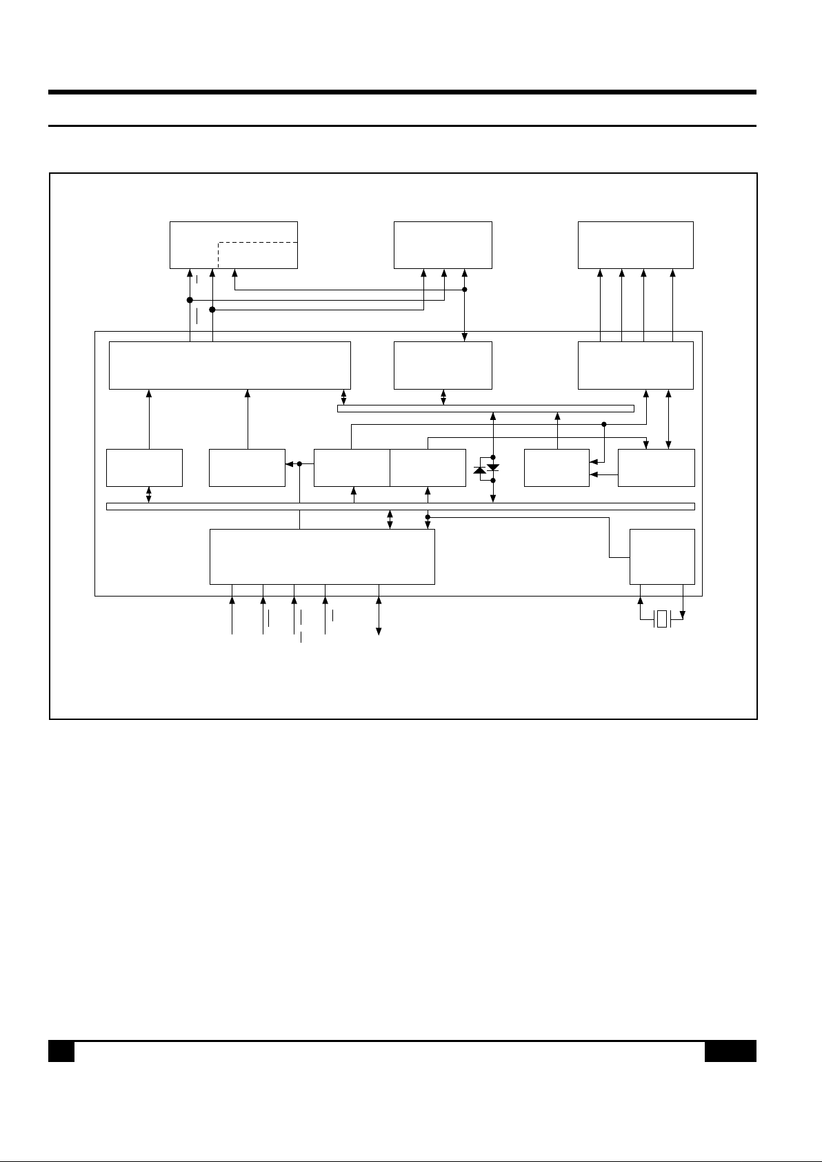
1.3 Block Diagram
Figure 1. SED1330F block diagram
Video RAM
Character
Generator RAM
Character
Generator ROM
LCD
LCD Controller
Input/Output
Register
Video RAM Interface
Display
Address
Controller
Cursor
Address
Controller
Refresh
Counter
Dot Counter
Layered
Controller
Character
Generator
ROM
OscillatorMicroprocessor Interface
YSCL,YD,YDIS
LP, WF
XSCL, XECL
XD0 to XD3
VD0 to VD7
VA0 to VA15
VCE
VR/W
SEL1
SEL0
RES
RD, WR
A0, CS
D0 to D7
OSC1 OSC2
S-MOS Systems, Inc. • 2460 North First Street • San Jose, CA 95131 • Tel: (408) 922-0200 • Fax: (408) 922-0238
268-0.4 13
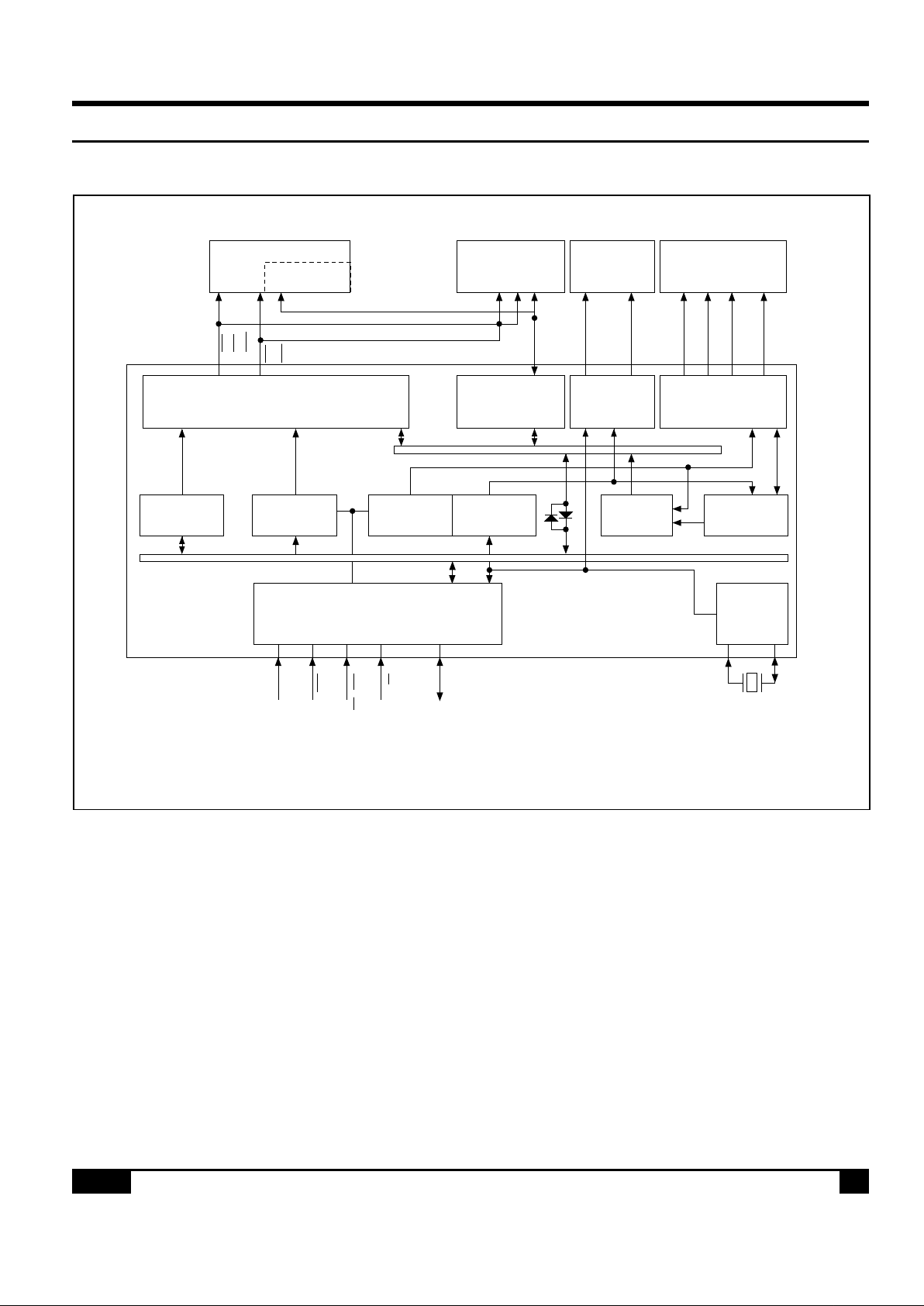
1.3 Block Diagram
Figure 2. SED1335F/1336F block diagram
1.3 1.0 Overview
Video RAM
Character
Generator RAM
Character
Generator ROM
LCD ControllerVideo RAM Interface
Display
Address
Controller
Cursor
Address
Controller
Refresh
Counter
Dot Counter
Character
Generator
ROM
Layered
Controller
OscillatorMicroprocessor Interface
YSCL, YD, YDIS
LP, WF
XSCL, XECL
XD0 to XD3
VD0 to VD7
VA0 to VA15
VCE,
VRD,
VWR
VRD
VWR
SEL1
SEL0
RES
RD, WR
A0, CS
D0 to D7
XG
XD
TV
Controller*
Input/Output
Register
TV LCD
VSD
SNC
*SED1336F only
S-MOS Systems, Inc. • 2460 North First Street • San Jose, CA 95131 • Tel: (408) 922-0200 • Fax: (408) 922-0238
14 268-0.4
1.0 Overview 1.4 – 1.4.2
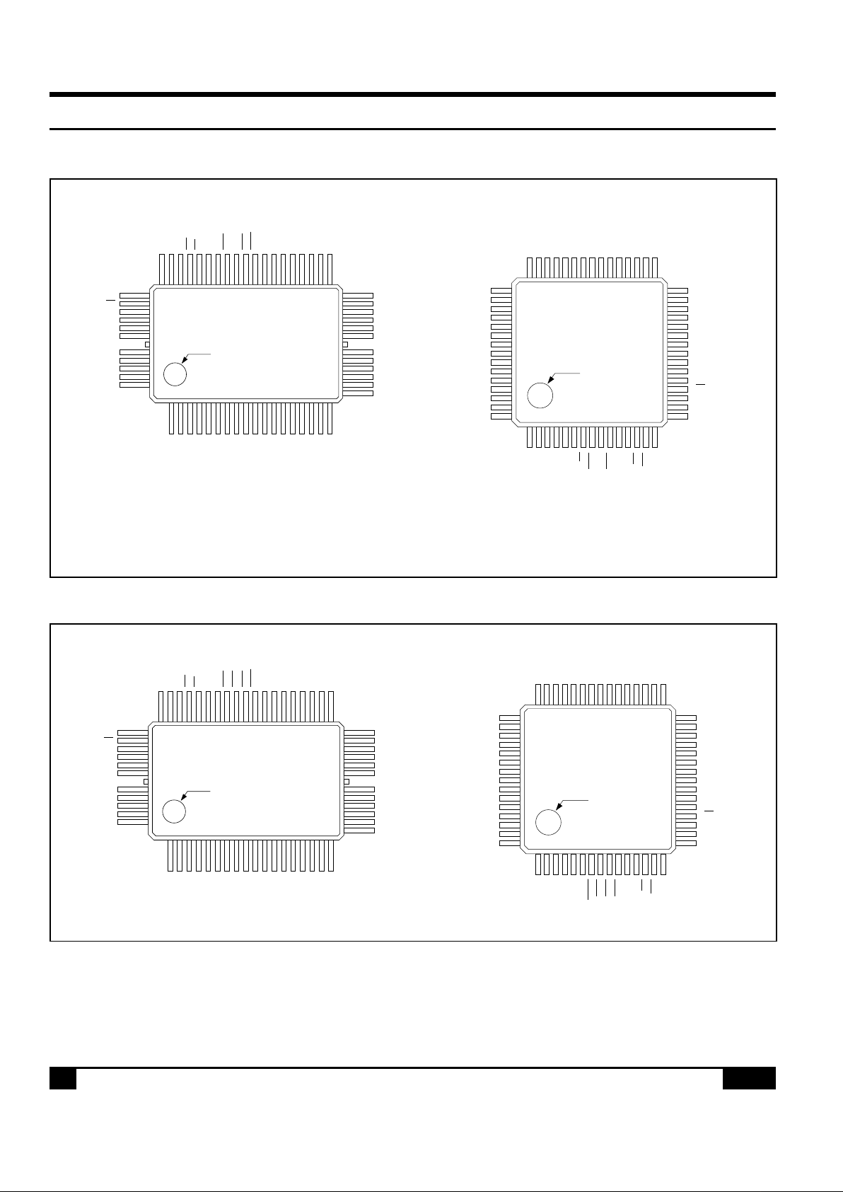
1.4 Pinouts
Index
115
3145
46
60
SED1330FBB
16
30
XD3
D7
D6
D5
D4
D3
D2
D1
D0
V
DD
A0
CS
OSC2
OSC1
SEL 1
VD3
VD2
VD1
VD0
VA15
VA14
VA13
VA12
VA11
VA10
VA9
VA8
VA7
VA6
NC
VD4
VD5
VD6
VD7
YSCL
YD
YDIS
WF
LP
V
SS
XSCL
XECL
XD0
XD1
XD2
VA5
VA4
VA3
VA2
VA1
VA0
VR/W
VCE
NC
RES
NC
NC
RD
WR
SEL 2
Index
55
1
30
60
5
29
404550
201510
SED1330F
BA
VA8
VA9
VA10
VA11
VA12
VA13
NC
VA14
VA15
VD0
VD1
VD2
XD
CS
A0
V
DD
D0
D1
D2
D3
D4
D5
D6
D7
XD3
XD2
XD1
XD0
XECL
XSCL
V
SS
LP
WF
YDIS
YD
YSCL
VD7
VD6
VD5
VD4
VD3
XG
SEL1
SEL2WRRDNCNC
RESNCVCE
VWR
VA0
VA1
VA2
VA3
VA4
VA5
VA6
VA7
6
Figure 3. SED1330F and SED1335F pinouts
Index
115
3145
46
60
SED1335F0B
(SED1336F0A)
16
30
XD3
D7
D6
D5
D4
D3
D2
D1
D0
V
DD
A0
CS
XD
XG
SEL1
VD3
VD2
VD1
VD0
VA15
VA14
VA13
VA12
VA11
VA10
VA9
VA8
VA7
VA6
NC
VD4
VD5
VD6
VD7
YSCL(SNC)
YD
YDIS
WF
LP
V
SS
XSCL
XECL(VSD)
XD0
XD1
XD2
VA5
VA4
VA3
VA2
VA1
VA0
VWR
VCE
VRD
RES
NC
NC(CLO)
RD
WR
SEL 2(NT/PL)
Index
55
1
30
60
5
29
404550
201510
SED1335F
OA
VA8
VA9
VA10
VA11
VA12
VA13
NC
VA14
VA15
VD0
VD1
VD2
XD
CS
A0
V
DD
D0
D1
D2
D3
D4
D5
D6
D7
XD3
XD2
XD1
XD0
XECL
XSCL
V
SS
LP
WF
YDIS
YD
YSCL
VD7
VD6
VD5
VD4
VD3
XG
SEL1
SEL2
WR
RD
NC
NC
RES
VRD
VCE
VWR
VA0
VA1
VA2
VA3
VA4
VA5
VA6
VA7
6
S-MOS Systems, Inc. • 2460 North First Street • San Jose, CA 95131 • Tel: (408) 922-0200 • Fax: (408) 922-0238
268-0.4 15
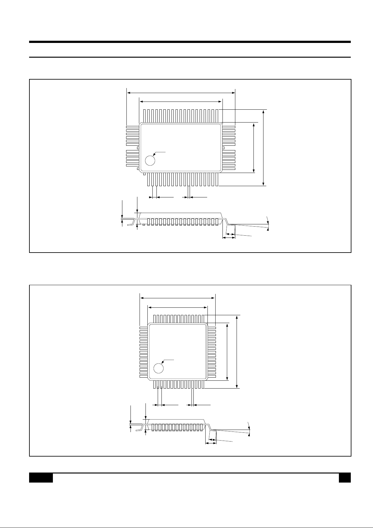
1.5 Package Dimensions
QFP5 Unit: mm
Figure 5. SED1330F
BB
, 1335F0B and SED1336F
0A
QFP6 Unit: mm
Index
115
31
16
45
46
60
30
0 ~ 12°
1.8
2.7
±
0.1
0.8 ±
0.3
0.15
±
0.05
0.35 ±
0.15
0.8 ±
0.15
17.6
±
0.4
14.0
±
0.2
17.6 ±
0.4
14.0 ±
0.2
0 ~ 12°
2.8
2.7
±
0.1
1.5 ±
0.3
0.15
±
0.05
Index
623
36
24
54
55
1
30
0.35 ±
0.1
19.6
±
0.4
14.0
±
0.1
25.6 ±
0.4
20.0 ±
0.1
60
5
29
35
1.0 ±
0.1
Figure 4. SED1330F
BA
and 1335F0A package dimensions
1.4 – 1.4.2 1.0 Overview

S-MOS Systems, Inc. • 2460 North First Street • San Jose, CA 95131 • Tel: (408) 922-0200 • Fax: (408) 922-0238
16 268-0.4
THIS PAGE INTENTIONALLY BLANK

S-MOS Systems, Inc. • 2460 North First Street • San Jose, CA 95131 • Tel: (408) 922-0200 • Fax: (408) 922-0238
268-0.4 17
2.0
Pin Description
S-MOS Systems, Inc. • 2460 North First Street • San Jose, CA 95131 • Tel: (408) 922-0200 • Fax: (408) 922-0238
18 268-0.4
2.0 Pin Description
2.1 SED1330F
BA/BB
Pin Summary
2.0 Pin Description 2.0 – 2.1
Name
Number
Type Description
SED1330F
0A SED1330FBB
VA0 to VA15
27 to 28 50 to 59
Output VRAM address bus
30 to 43 1 to 6
VR/W 44 7 Output VRAM write signal
VCE 45 8 Output Memory control signal
RES 47 10 Input Reset
NC 29, 46, 48, 49 9, 11, 12, 60 — No connection
RD 50 13 Input
8080 family: Read signal
6800 family: Enable clock (E)
WR 51 14 Input
8080 family: Write signal
6800 family: R/W signal
SEL2 52 15 Input
8080 or 6800 family interface
select
SEL1 53 16 Input
8080 or 6800 family interface
select
OSC1 54 17 Input Oscillator connection
OSC2 55 18 Output Oscillator connection
CS 56 19 Input Chip select
A0 57 20 Input Data type select
V
DD 58 21 Supply 4.5 to 5.5V supply
D0 to D7
59 to 60
22 to 29 Input/output Data bus
1 to 6
XD0 to XD3 10 to 7 33 to 30 Output X-driver data
XECL 11 34 Output X-driver enable chain clock
XSCL 12 35 Output X-driver data shift clock
V
SS 13 36 Supply Ground
LP 14 37 Output Latch pulse
WF 15 38 Output Frame signal
YDIS 16 39 Output
Power-down signal when display is
blanked
YD 17 40 Output Scan start pulse
YSCL 18 41 Output Y-driver shift clock
VD0 to VD7 26 to 19 49 to 42 Input/output VRAM data bus
S-MOS Systems, Inc. • 2460 North First Street • San Jose, CA 95131 • Tel: (408) 922-0200 • Fax: (408) 922-0238
268-0.4 19
2.0 – 2.2 2.0 Pin Description
2.0 Pin Description
2.2 SED1330F/1335F
0A/0B
Pin Summary
Name
Number
Type Description
SED1335F
0A SED1335F0B
VA0 to VA15
27 to 28 50 to 59
Output VRAM address bus
30 to 43 1 to 6
VWR 44 7 Output VRAM write signal
VCE 45 8 Output Memory control signal
VRD 46 9 Output VRAM read signal
RES 47 10 Input Reset
NC 29, 48, 49 11, 12, 60 — No connection
RD 50 13 Input
8080 family: Read signal
6800 family: Enable clock (E)
WR 51 14 Input
8080 family: Write signal
6800 family: R/W signal
SEL2 52 15 Input
8080 or 6800 family interface
select
SEL1 53 16 Input
8080 or 6800 family interface
select
XG 54 17 Input Oscillator connection
XD 55 18 Output Oscillator connection
CS 56 19 Input Chip select
A0 57 20 Input Data type select
V
DD 58 21 Supply 2.7 to 5.5V supply
D0 to D7
59 to 60
22 to 29 Input/output Data bus
1 to 6
XD0 to XD3 10 to 7 33 to 30 Output X-driver data
XECL 11 34 Output X-driver enable chain clock
XSCL 12 35 Output X-driver data shift clock
V
SS 13 36 Supply Ground
LP 14 37 Output Latch pulse
WF 15 38 Output Frame signal
YDIS 16 39 Output
Power-down signal when display is
blanked
YD 17 40 Output Scan start pulse
YSCL 18 41 Output Y-driver shift clock
VD0 to VD7 26 to 19 49 to 42 Input/output VRAM data bus
S-MOS Systems, Inc. • 2460 North First Street • San Jose, CA 95131 • Tel: (408) 922-0200 • Fax: (408) 922-0238
20 268-0.4
2.0 Pin Description 2.3
2.3 SED1336F0A Pin Summary
Name Number Type Description
VA0 to VA15
1 to 6
Output VRAM address bus
50 to 59
VWR 7 Output VRAM write signal
VCE 8 Output Memory control signal
VRD 9 Output VRAM read signal
RES 10 Input Reset
NC 11, 60 — No connection
CLO 12 Output Clock output
RD 13 Input
8080 family: Read signal
6800 family: Enable clock (E)
WR 14 Input
8080 family: Write signal
6800 family: R/W signal
NT/PL 15 Input NTSC or PAL TV mode select
SEL1 16 Input 8080 or 6800 family interface select
OSC1 17 Input Oscillator connection
OSC2 18 Output Oscillator connection
CS 19 Input Chip select
A0 20 Input Data type select
V
DD 21 Supply 3.0 to 5.5V supply
D0 to D7 22 to 29 Input/output Data bus
XD0 to XD3 30 to 33 Output X-driver data
VSD 34 Output Video data
XSCL 35 Output Data shift clock
VSS 36 Supply Ground
LP 37 Output Latch pulse
WF 38 Output Frame signal
YDIS 39 Output
Power-down signal when display is
blanked
YD 40 Output Scan start pulse
SNC 41 Output TV sync signal
VD0 to VD7 42 to 49 Input/output VRAM data bus
S-MOS Systems, Inc. • 2460 North First Street • San Jose, CA 95131 • Tel: (408) 922-0200 • Fax: (408) 922-0238
268-0.4 21
2.4 – 2.4.3 2.0 Pin Description
2.4 Pin Functions
2.4.1 Power Supply
Pin Name Function
V
DD
4.5 to 5.5V (SED1330F), 3.0 to 5.5V (SED1336F) or 2.7 to 5.5V (SED1330F/1335F) supply.
This may be the same supply as the controlling microprocessor.
V
SS Ground
Note: The peak supply current drawn by the SED1330F/1335F/1336F may be up to ten times the average supply current. The power
supply impedance must be kept as low as possible by ensuring that supply lines are sufficiently wide and by placing 0.47 µF
decoupling capacitors that have good high-frequency response near the device’s supply pins.
2.4.3 Microprocessor Interface
Pin Name Function
D0 to D7 Tristate input/output pins. Connect these pins to an 8- or 16-bit microprocessor bus.
Microprocessor interface select pin. The SED1336F supports both 8080 family processors
(such as the 8085 and Z80®) and 6800 family processors (such as the 6802 and 6809).
SEL1* SEL2 Interface A0 RD WR CS
0 0 8080 family A0 RD WR CS
1 0 6800 family A0 E R/W CS
* SED1330F and SED1335F only
Note: SEL1 should be tied directly to VDD or VSS to prevent noise. If noise does appear on SEL1, decouple it to ground using a
capacitor placed as close to the pin as possible.
SEL1, SEL2
2.4.2 Oscillator
Pin Name Function
(OSC) XG
Crystal connection for internal oscillator (see Section 8.3). This pin can be driven by an external
clock source that satisfies the timing specifications of the EXT φ0 signal (see Section 4.3.6).
(OSC2) XD
Crystal connection for internal oscillator. Leave this pin open when using an external clock
source.
CLO
Clock output (SED1336F only). Same phase as XG. Clock is output when system command
P1 is executed. Output stops during system reset.
S-MOS Systems, Inc. • 2460 North First Street • San Jose, CA 95131 • Tel: (408) 922-0200 • Fax: (408) 922-0238
22 268-0.4
2.0 Pin Description 2.4.3
Pin Name Function
A0, in conjunction with the RD and WR or R/W and E signals, controls the type of access to
the SED1336F, as shown below.
8080 family interface
A0 RD WR Function
0 0 1 Status flag read
1 0 1 Display data and cursor address read
0 1 0 Display data and parameter write
1 1 0 Command write
6800 family interface
A0 R/W E Function
0 1 1 Status flag read
1 1 1 Display data and cursor address read
0 0 1 Display data and parameter write
1 0 1 Command write
When the 8080 family interface is selected, this signal acts as the active-LOW read strobe. The
SED1330F/1335F/1336F’s output buffers are enabled when this signal is active.
When the 6800 family interface is selected, this signal acts as the active-HIGH enable clock.
Data is read from or written to the SED1330F/1335F/1336F when this clock goes HIGH.
When the 8080 family interface is selected, this signal acts as the active-LOW write strobe. The
bus data is latched on the rising edge of this signal.
When the 6800 family interface is selected, this signal acts as the read/write control signal. Data
is read from the SED1330F/1335F/1336F if this signal is HIGH, and written to the SED1330F/
1335F/1336F if it is LOW.
Chip select. This active-LOW input enables the SED1330F/1335F/1336F. It is usually
connected to the output of an address decoder device that maps the SED1330F/1335F/1336F
into the memory space of the controlling microprocessor.
This active-LOW input performs a hardware reset on the SED1330F/1335F/1336F. It is a
Schmitt-trigger input for enhanced noise immunity; however, care should be taken to ensure
that it is not triggered if the supply voltage is lowered.
WR or R/W
CS
RES
RD or E
A0
S-MOS Systems, Inc. • 2460 North First Street • San Jose, CA 95131 • Tel: (408) 922-0200 • Fax: (408) 922-0238
268-0.4 23
2.4.4 – 2.4.5 2.0 Pin Description
2.4.4 Display Memory Control
The SED1330F/1335F/1336F can directly access static
RAM and PROM. The designer may use a mixture of
these two types of memory to achieve an optimum
trade-off between low cost and low power consumption.
Pin Name Function
VA0 to VA15
16-bit display memory address. When accessing character generator RAM or ROM, VA0 to
VA3, reflect the lower 4 bits of the row counter.
VD0 to VD7 8-bit tristate display memory data bus. These pins are enabled when VR/W is LOW.
VR/W Active-LOW display memory write control output (SED1330).
VRD Active-LOW display memory read control output (SED1335/6).
VCE Active-LOW static memory standby control signal. VCE can be used with CS.
VWR Active-LOW display memory write control output (SED1335/6).
2.4.5 LCD Drive Signals
In order to provide effective low-power drive for LCD
matrixes, the SED1330F/1335F/1336F can directly
control both the X- and Y-drivers using an enable
chain.
Pin Name Function
XD0 to XD3
4-bit X-driver (column drive) data outputs. Connect these outputs to the inputs of the X-driver
chips.
The falling edge of XSCL latches the data on XD0 to XD3 into the input shift registers of the
X-drivers. To conserve power, this clock halts between LP and the start of the following display
line (see Section 4.3.7).
XECL
The falling edge of XECL (SED1330F/1335F only) triggers the enable chain cascade for the
X-drivers (SED1600/SED1180). Every 16th clock pulse is output to the next X-driver.
LP latches the signal in the X-driver shift registers into the output data latches. LP is a fallingedge triggered signal, and pulses once every display line.
Connect LP to the Y-driver shift clock on modules that use the SED1600 and SED1610 drivers.
WF
LCD panel AC drive output. The WF period is selected to be one of two values with SYSTEM
SET command.
The falling edge of YSCL (SED1330F/1335F only) latches the data on YD into the input shift
registers of the Y-drivers. YSCL is not used with the SED1600, SED1610 or other driver ICs
which use LP as the Y-driver shift clock.
YD is the data pulse output for the Y drivers. It is active during the last line of each frame, and
is shifted through the Y drivers one by one (by YSCL), to scan the display’s common
connections.
Power-down output signal. YDIS is HIGH while the display drive outputs are active.
YDIS goes LOW one or two frames after the sleep command is written to the SED1330F/
1335F/1336F. All Y-driver outputs are forced to an intermediate level (de-selecting the display
segments) to blank the display. In order to implement power-down operation in the LCD unit,
the LCD power drive supplies must also be disabled when the display is disabled by YDIS.
XSCL
LP
YSCL
YD
YDIS

S-MOS Systems, Inc. • 2460 North First Street • San Jose, CA 95131 • Tel: (408) 922-0200 • Fax: (408) 922-0238
24 268-0.4
1.0 Overview 1.3
THIS PAGE INTENTIONALLY BLANK

S-MOS Systems, Inc. • 2460 North First Street • San Jose, CA 95131 • Tel: (408) 922-0200 • Fax: (408) 922-0238
268-0.4 25
1.3 – 1.4 1.0 Overview
3.0
Command Description

S-MOS Systems, Inc. • 2460 North First Street • San Jose, CA 95131 • Tel: (408) 922-0200 • Fax: (408) 922-0238
26 268-0.4
THIS PAGE INTENTIONALLY BLANK

S-MOS Systems, Inc. • 2460 North First Street • San Jose, CA 95131 • Tel: (408) 922-0200 • Fax: (408) 922-0238
268-0.4 27
3.0 – 3.1 3.0 Command Description
3.0 Command Description
3.1 The Command Set
Table 1. The Command Set
Command
Code Read
Class Command Hex Command Description
Parameters
RD WR A0 D7 D6 D5 D4 D3 D2 D1 D0
No. of SecBytes tion
SYSTEM SET 1010100000040
Initialize device and dis-
8 3.2.1
play
SLEEP IN 1010101001153Enter standby mode 0 3.2.2
DISP ON/OFF 1010101100D
58, Enable and disable dis-
1 3.3.1
59 play and display flashing
SCROLL 1010100010044
Set display start address
10 3.3.2
and display regions
CSRFORM 101010111015DSet cursor type 2 3.3.3
CGRAM ADR 101010111005C
Set start address of char-
2 3.3.6
acter generator RAM
CD CD
4C
Set direction of cursor
CSRDIR 101010011
10
to
movement
0 3.3.4
4F
HDOT SCR 101010110105A
Set horizontal scroll pos-
1 3.3.7
ition
OVLAY 101010110115B
Set display overlay for-
1 3.3.5
mat
CSRW 1010100011046Set cursor address 2 3.4.1
CSRR 1010100011147Read cursor address 2 3.4.2
MWRITE 1010100001042Write to display memory — 3.5.1
MREAD 1010100001143
Read from display mem-
— 3.5.2
ory
Notes:
1. In general, the internal registers of the SED1330F/1335F/1336F are modified as each command parameter is input. However,
the microprocessor does not have to set all the parameters of a command and may send a new command before all parameters
have been input. The internal registers for the parameters that have been input will have been changed but the remaining
parameter registers are unchanged.
2-byte parameters (where two bytes are treated as one data item) are handled as follows:
a. CSRW, CSRR: Each byte is processed individually. The microprocessor may read or write just the low byte of the cursor
address.
b. SYSTEM SET, SCROLL, CGRAM ADR: Both parameter bytes are processed together. If the command is changed after
half of the parameter has been input, the single byte is ignored.
2. APL and APH are 2-byte parameters, but are treated as two 1-byte parameters.
System
control
Display
control
Drawing
control
Memory
control

S-MOS Systems, Inc. • 2460 North First Street • San Jose, CA 95131 • Tel: (408) 922-0200 • Fax: (408) 922-0238
28 268-0.4
3.0 Command Description 3.2 – 3.2.1
3.2 System Control Commands
3.2.1 SYSTEM SET
Initializes the device, sets the window sizes, and
selects the LCD interface format. Since the command
sets the basic operating parameters of the SED1330F/
1335F/1336F, an incorrect SYSTEM SET command
may cause other commands to operate incorrectly.
C 01000000 1 0 1
D7 D6 D5 D4 D3 D2 D1 D0 A0 WR RD
P1 DR T/L IV 1 W/S M2 M1 M0 0 0 1
P2 WF0000 FX 0 0 1
P3 0000 FY 0 0 1
P4 C/R 0 0 1
P5 TC/R 0 0 1
P6 L/F 0 0 1
P7 APL 0 0 1
P8 APH 0 0 1
LSBMSB
Figure 7. SYSTEM SET instruction

S-MOS Systems, Inc. • 2460 North First Street • San Jose, CA 95131 • Tel: (408) 922-0200 • Fax: (408) 922-0238
268-0.4 29
3.2.1.1 – 3.2.1.5 3.0 Command Description
3.2.1.1 C
This control byte performs the following:
1. Resets the internal timing generator
2. Disables the display
3. Cancels sleep mode
Parameters following P1 are not needed if only canceling sleep mode.
3.2.1.2 M0
Selects the internal or external character generator
ROM. The internal character generator ROM contains 160, 5 × 7 pixel characters. These characters are
fixed at fabrication by the metalization mask. The
external character generator ROM can contain up to
256 user-defined characters.
M0 = 0: Internal CG ROM
M0 = 1: External CG ROM
Note that if the CG ROM address space overlaps the
display memory address space, that portion of the
display memory cannot be written to.
3.2.1.3 M1
Selects the CG RAM area for user-definable characters. The CG RAM codes are selected from the 64
codes shown in Figure 59.
M1 = 0: CG RAM1; 32 char
The CG RAM1 and CG RAM2 address spaces are not
contiguous, the CG RAM1 address space is treated
as character generator RAM, and the CG RAM2
address space is treated as character generator ROM.
M1 = 1: 64 char CG RAM + CG RAM2
The CG RAM1 and CG RAM2 address spaces are
contiguous and are both treated as character generator RAM.
3.2.1.4 M2
Selects the height of the character defined in external
CG ROM and CG RAM. Characters more than 16 pixels high can be displayed by creating a bitmap for
each portion of each character and using the
SED1330F/1335F/1336F’s graphics mode to reposition them.
M2 = 0: 8-pixel character height (2716 or
equivalent ROM)
M2 = 1: 16-pixel character height (2732
or equivalent ROM)
3.2.1.5 W/S
Selects the LCD drive method.
W/S = 0: Single-panel drive
W/S = 1: Dual-panel drive
S-MOS Systems, Inc. • 2460 North First Street • San Jose, CA 95131 • Tel: (408) 922-0200 • Fax: (408) 922-0238
30 268-0.4
3.0 Command Description 3.2.1.5
Figure 8. Single-panel display
Figure 9. Dual-panel display
EI
X driver X driver
LCD
Y driver
YD
EI
X driver X driver
YD
X driver X driver
Upper Panel
Lower Panel
Y driver
 Loading...