

Page 1
User manual of F-USB-US-V1
1. Introduction
F-USB-US-V1 is a ZigBee/ Z-wave Combo module compliant with IEEE802.15.4 MAC/baseband/radio and
ITU-T G.9959 optimized for low-power applications.
The ZigBee chipset is from Silicon Labs, part number EM3588-RT and Z-wave chipset is from Sigma Designs,
part number SD3503.
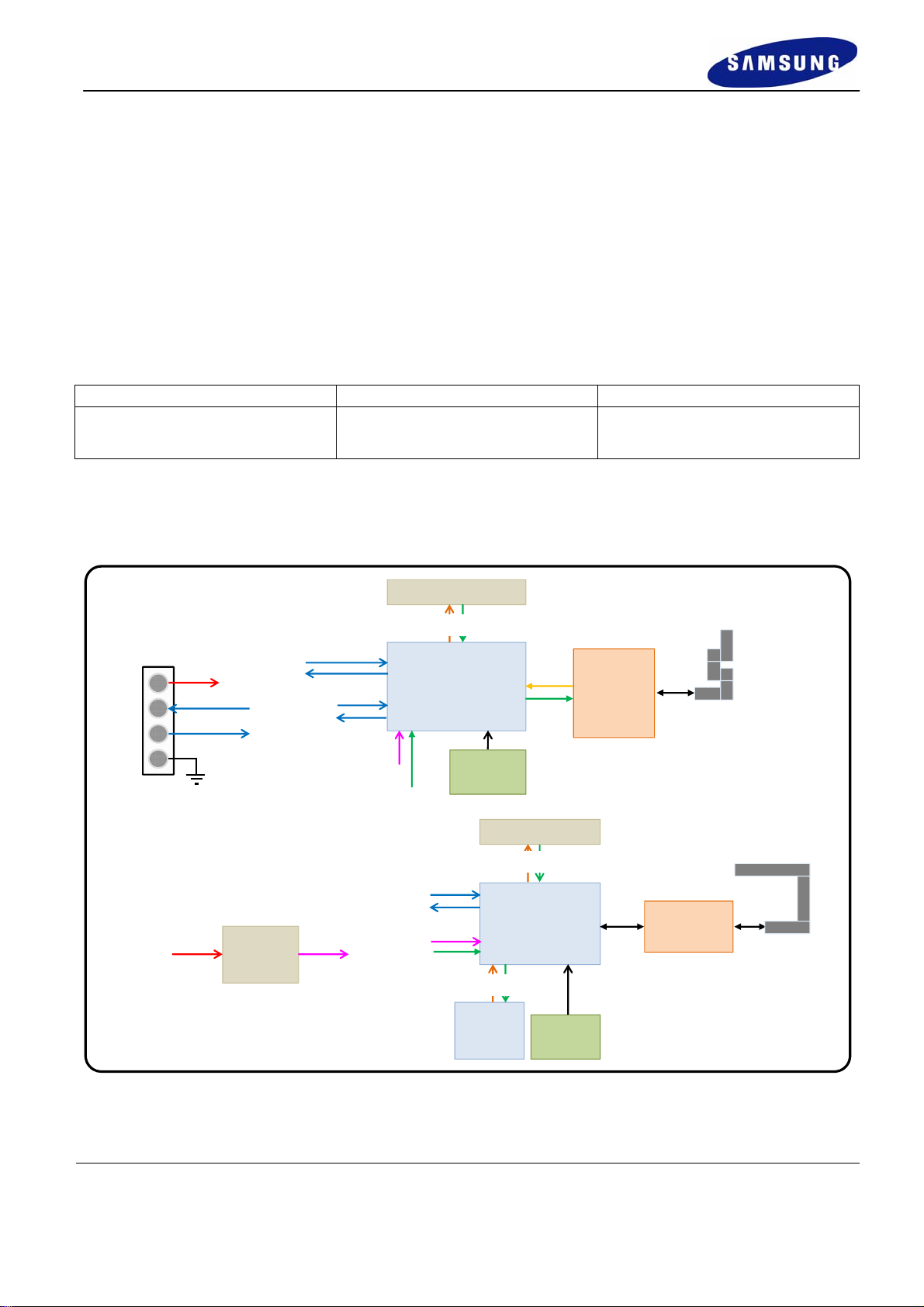
2. Hardware Architecture:
2.1 Main Chipset Information
Item Vendor Part Number
IEEE802.15.4
ITU-T G.9959
Silicon Labs
Sigma Designs
2.2 Circuit Block Diagram
The major internal and external block diagram of F-USB-US-V1
is illustrated in Figure 1-1.
EM3588-RT
SD3503
D/L Port(TP)
2.4GHz PCB pattern
Antenna
900MHz PCB pattern
Antenna
SAW Filter
(BW:25M Hz)
VBUS(+5V)
USB DP
USB DM
GND
USB Connector
VBUS(+5V)
DC-DC
Convertor
+3.3V
USB
UART
+3.3V
ZigBee Single-Chip
(EM3588-RT)
NRESET
ISP(10p)
UART
+3.3V
RESETN
X-tal
(24MHz)
SPI
F-MEM
(2Mbit)
FEM
(SE2432L)
D/L Port(TP)
(10pin)
Z-wave SoC
(SD3503)
X-tal
(32MHz)
Figure 1-1 F-USB-US-V1
block diagram and System Interface
Version 1.0 Samsung Electronics page 1 of 10
Page 2

3. Operational Description
F-USB-US-V1 is the 802.15.4 ZigBee, ITU-T G.9959 Z-wave COMBO Module that acts as a
communication controller for users of a wireless device to connect to SMART TV
- Features
> ZigBee 2.4GHz IEEE 802.15.4
>
AES128 encryption accelerator
> Low power consumption, advanced management
>On-chip power amplifiers and low –noise amplifiers for both bands
> Z-Wave ITU-T G.9959
> Z-Wave 9.6/40/100 kbit/s data rate
>128-bit AES security processor and hardware random number generator
- Time base of the RF frequency
For ZigBee IF and RF frequency, a crystal(24MHz) is a clock reference.
For Z-wave IF and RF frequency, a crystal(32MHz) is a clock reference.
- ZigBee Transmission
The ZigBee Tx path produces an O-QPSK-modulated signal using the analog front end and digital
baseband. The area- and power-efficient Tx architecture uses a two-point modulation scheme to modulate
the RF signal generated by the synthesizer. The modulated RF signal is fed to the integrated PA and then
out of the EM357.
- ZigBee Receiver
The ZigBee Rx path uses a low-IF, super-heterodyne receiver that rejects the image frequency using
complex mixing and polyphase filtering. In the analog domain, the input RF signal from the antenna is first
amplified and mixed down to a 4 MHz IF frequency. The mixers’ output is filtered, combined, and
amplified before being sampled by a 12 MSPS ADC. The digitized signal is then demodulated in the digital
baseband. The filtering within the Rx path improves the EM35x’s co-existence with other 2.4 GHz
transceivers such as Zigbee/ 802.15.4-2003, IEEE 802.11-2007, and Bluetooth radios. The digital baseband
also provides gain control of the Rx path, both to enable the reception of small and large wanted signals
and to tolerate large interferers.
- Z-wave Tranceiver
The F-USB-US-V1 is a fully integrated module with an on-board antenna that allows the establishment of
a Z-Wave network with minimum risk. The SD3503 chip is used with an external NVM (Serial Flash
MEM), 32MHz crystal, power supply decoupling, SAW filter, matching circuit, and a PCB pattern Antenna.
Version 1.0 Samsung Electronics page 2 of 10
Page 3
- Product Details
> Data Modulation
ZigBee : O-QPSK for 802.15.4
Z-Wave : FSK/GFSK for
ITU-T G.9959
> Frequency :
ZigBee
Channel 0x0B(11ch ) 2405 MHz
Channel 0x0C(12ch) 2410 MHz
Channel 0x0D(13ch) 2415 MHz
Channel 0x0E(14ch) 2420 MHz
Channel 0x0F(15ch) 2425 MHz
Channel 0x10(16ch) 2430 MHz
Channel 0x11(17ch) 2435 MHz
Channel 0x12(18ch) 2440 MHz
Channel 0x13(19ch) 2445 MHz
Channel 0x14(20ch) 2450 MHz
Channel 0x15(21ch) 2455 MHz
Channel 0x16(22ch) 2460 MHz
Channel 0x17(23ch) 2465 MHz
Channel 0x18(24ch) 2470 MHz
Channel 0x19(25ch) 2475 MHz
Channel 0x1A(26ch) 2480 MHz
Z-wave
Version 1.0 Samsung Electronics page 3 of 10
Page 4

- Product pwr Spec.
Symbol Parameter Min Typ. Max Unit
VDD Power supply 4.5 5 5.5 V
- Product Spec.
> ZigBee
Parameter Min Typ. Max Unit
RF Characteristics
RF Frequency Range 2.405 - 2.4835 GHz
TX Frequency Tolerance -74.4 - 74.4 KHz
TX Spurious Emission
30.0MHz to 2.395GHz
2.495GHz to 12.75GHz
- - -30 dBm
TX Harmonics
Error Vector Magnitude(EVM) - - 35 %
RX sensitivity
RX Spurious Emission
nd
2
Harmonics
rd
3
Harmonics
PER at -85dBm
30.0MHz to 12.5GHz
- - -30 dBm
- - 1 %
- - -54 dBm
Frequency Power setting Level
2405 MHz -2
2440 MHz -2
2475 MHz -5
2480 MHz -16
Version 1.0 Samsung Electronics page 4 of 10
Page 5

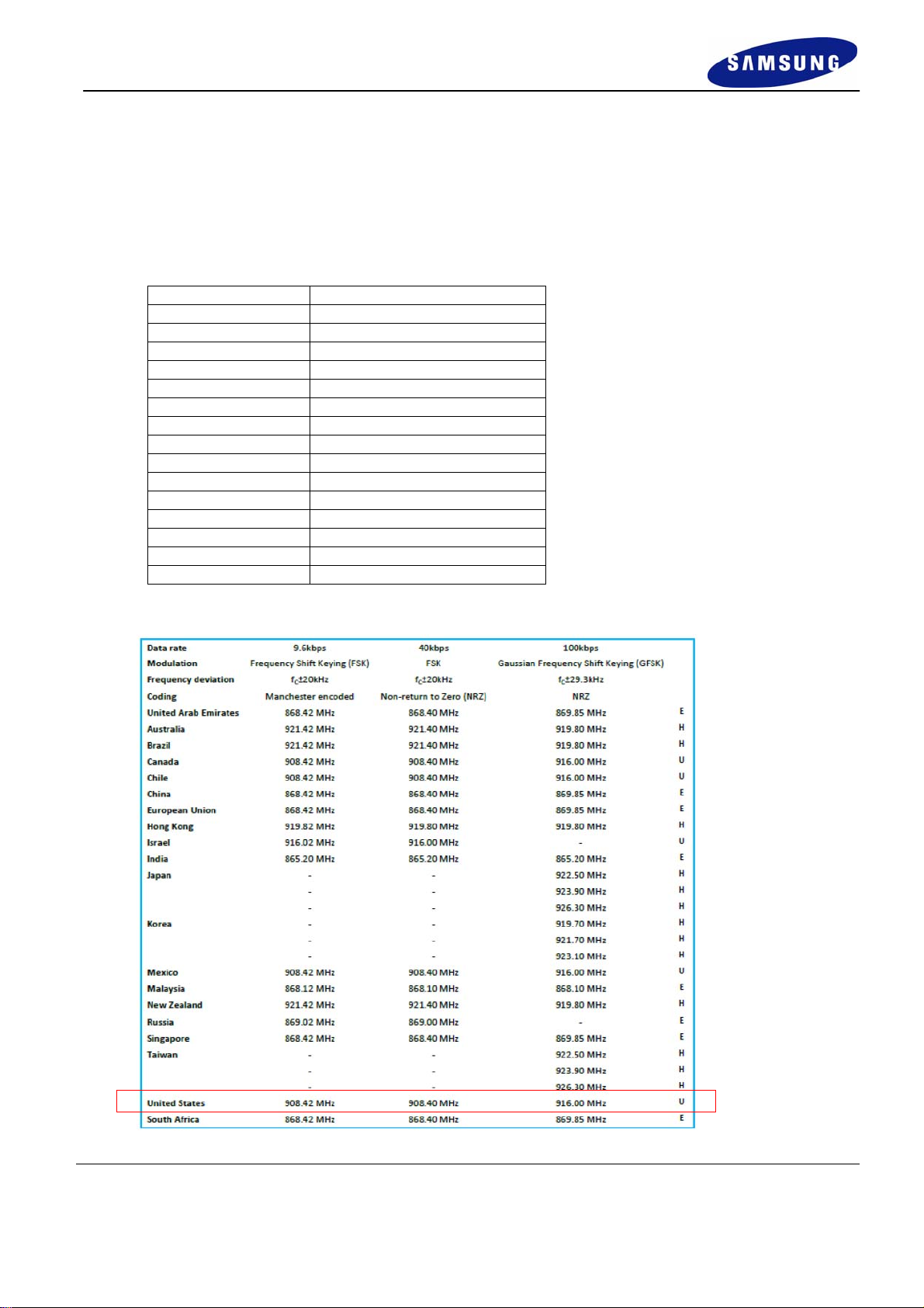
> Z-wave
Parameter Min Typ. Max Unit
RF Characteristics(NA)
RF Frequency Range 868.40 - 923.1 MHz
TX Frequency Tolerance -25.0 - 25.0 KHz
TX Harmonics
RX sensitivity
RX Spurious Emission
Frequency
(MHz)
908.40 10
908.42 11
916.00 15
nd
2
Harmonics
rd
3
Harmonics
PER at -85dBm
30.0MHz to 12.5GHz
Power
Setting
- - -30 dBm
- - 3 %
- - -54 dBm
4. Installation Guide
- Installation Figure
< USB Dongle >
Version 1.0 Samsung Electronics page 5 of 10
Page 6

Version 1.0 Samsung Electronics page 6 of 10
Page 7

5. Notice
FCC Statement
This device complies with Part 15 of FCC Rules, Operation is Subject to following two conditions:
(1) This device may not cause harmful interference, and
(2) This device must accept any interference received including interferenc e that cause undesired
operation.
This equipment has been tested and found to comply within the limits for a Class B digital device,
pursuant to part 15 of the FCC Rules. These limits are designed to provide reasonable protection against
harmful interference in a residential installation.
This equipment generates, uses, and can radiate radio frequency energy and, if not installed and used in
accordance with the instructions, may cause harmful interference to radio communications. However, there is
no guarantee that interference will not occur in a particular installation. If this equipment does cause harmfu l
interference to radio or television reception, which can be determined by turning the equipment off and on, the
user is encouraged to try to correct the interference by one or more of the following measures:
• Reorient or relocate the receiving antenna
• Increase the separation between the equipment and receiver
• Connect the equipment into an outlet on a different circuit from that to which the receiver is connected
• Consult the dealer or an experienced radio/TV technician for help.
This device and its antenna(s) must not be co-located or operation in conjunction with any other antenna or
transmitter.
IMPORTANT NOTE:
FCC Radiation Exposure Statement;
This equipment complies with FCC radiation exposure limits set forth for an uncontrolled environment.
This equipment should be installed and operated with minimum distance 2 0cm between the radiator & body.
IMPORTANT NOTE
This module is intended for OEM integrator. The OEM integrator is still responsible for the FCC compliance
Requirement of the end product, which integrates this module.
20cm minimum distance has to be able to be maintained between the antenna and the users for the host
this module is integrated into. Under such configuration, the FCC radiation exposure limits set forth for an
population / uncontrolled environment can be satisfied.
Any change or modifications not expressly approved by the manufacturer could avoid the user’s authority to
Operate this equipment.
Version 1.0 Samsung Electronics page 7 of 10
Page 8

USER MANUAL OF THE END PRODUCT:
In the users manual of the end of product, the end user has to be informed to keep at least 20cm separation
with the antenna while this end product is installed and operated.
The end user has to be informed that the FCC radio-frequency exposure guidelines for an uncontrolled
environment can be satisfied. The end user has to also be informed that any changes or modifications not
expressly approved by the manufacturer could void the user’s authority to operate this equipment.
if the size of the end product is smaller than 8x10cm,then additional FCC part15.19statement is required to be
available in the users manual; This device complies with Part15 of FCC rules.
LABEL OF THE END PRODUCT:
The final end product must be labeled in a visible area with the following " Contains TX FCC ID: R3YF-USB-USV1”
“If the size of the end product is larger than 8x10cm, then the following FCC part 15.19 statement has to also be
available on the label:
This device complies with Part 15 of FCC rules. Operation is subject to the following two conditions:
(1) this device may not cause harmful interference and (2) this device must accept any interference receiv ed,
including interference that may cause undesired operation.
Version 1.0 Samsung Electronics page 8 of 10
Page 9

IC Statement
This device complies with Industry Canada’s licence-exempt RSSs. Operation is subject to the following two
conditions:
(1) This device may not cause interference, and
(2) This device must accept any interference, including interference that may cause undesired operation of
the device.
Le présent appareil est conforme aux CNR d'Industrie Canada applicables aux appareils radio exempts de
licence. L'exploitation est autorisée aux deux conditions suivantes : (1) l'appareil ne doit pa s produire de
brouillage, et (2) l'utilisateur de l'appareil doit accepter tout brouillage radioélectrique subi, même si le brouillage
est susceptible d'en compromettre le fonctionnement.
This device and its antenna(s) must not be co-located or operation in conjunction with any other antenna or
transmitter.
The device could automatically discontinue transmission in case of absence of information to transmit, or
operational failure. Note that this is not intended to prohibit transmission of control or signaling information or
the use of repetitive codes where required by the technology.
IMPORTANT NOTE:
IC Radiation Exposure Statement:
This equipment complies with IC RSS-102 radiation exposure limits set forth for an uncontrolled environment.
This equipment should be installed and operated with minimum distance 20cm between the radiator & your
body.
IMPORTANT NOTE:
This module is intended for OEM integrator. The OEM integrator is still responsible for the IC compliance
requirement of the end product, which integrates this module.
20cm minimum distance has to be able to be maintained between the antenna and the users for the host this
module is integrated into. Under such configuration, the IC RSS- 102 radiation exposure limits set forth for an
population/uncontrolled environment can be satisfied.
Any changes or modifications not expressly approved by the manufacturer could void
the user's authority to operate this equipment.
Version 1.0 Samsung Electronics page 9 of 10
Page 10

USERS MANUAL OF THE END PRODUCT:
In the user manuals of the end product, the end user has to be informed to keep at least 20cm separatio n with
the antenna while this end product is installed and operated. The end user has to be informed that the IC radiofrequency exposure guidelines for an uncontrolled environment can be satisfied. The end user has to also be
informed that any changes or modifications not expressly approved by the manufacturer could void the
user's authority to operate this equipment. IC statement is required to be available in the user manuals:
This device complies with Industry Canada’s licence-exempt RSSs. Operation is subject to the following two
conditions:
(1) This device may not cause interference, and
(2) This device must accept any interference, including interference that may cause undesired operation of
the device.
LABEL OF THE END PRODUCT:
The final end product must be labeled in a visible area with the following " Contains TX IC:10734A-FUSBUSV1”
Version 1.0 Samsung Electronics page 10 of 10
 Loading...