

Page 1
ANALOG OUTPUTS MO DU LE
VOLTAGE / CURRENT
FEB / 01
DF46
DF46ME
Page 2

web: www.sma r.com
smar
BRAZIL
Smar Equipamentos Ind. Ltda.
Rua Dr. Antonio Furlan Jr., 1028
Sertãozinho SP 14170-480
Tel.: +55 16 3946-3510
Fax: +55 16 3946-3554
e-mail: insales@ smar.com.br
GERMANY
Smar Gm bH
Rheingaustrasse 9
55545 Bad Kreuznach
Germany
Tel: + 49 671-794680
Fax: + 49 671-7946829
e-mail: [email protected]
USA
Smar International Corporation
6001 Stonington Street, Suite 100
Houston, TX 77040
Tel.: +1 713 849-2021
Fax: +1 713 849-2022
e-mail: [email protected]
CHINA
Smar China Corp.
3 Baishiqiao Road, Suite 30233
Beijing 100873, P.R.C.
Tel.: +86 10 6849-8643
Fax: +86-10-6894-0898
e-mail: [email protected]
MEXICO
Smar Mexico
Cerro de las Campanas #3 desp 119
Col. San Andrés Atenco
Tlalnepantla Edo. Del Méx - C.P. 54040
Tel.: +53 78 46 00 al 02
Fax: +53 78 46 03
e-mail: [email protected]
Smar Laboratories Corporation
6001 Stonington Street, Suite 100
Houston, TX 77040
Tel.: +1 713 849-2021
Fax: +1 713 849-2022
e-mail: [email protected]
Specifications and information are subject to change without notice.
For the latest updates, please visit the SMAR website above.
FRANCE
Smar France S. A. R. L.
42, rue du Pavé des Gardes
F-92370 Chaville
Tel.: +33 1 41 15-0220
Fax: +33 1 41 15-0219
e-mail: [email protected]
SINGAPORE
Smar Singapore Pte. Ltd.
315 Outram Road
#06-07, Tan Boon Liat Building
Singapore 169074
Tel.: +65 6324-0182
Fax: +65 6324-0183
e-mail: [email protected]
Smar Research Corporation
4250 Veterans Memorial Hwy. Suite 156
Holbrook , NY 11741
Tel: +1-631-737-3111
Fax: +1-631-737-3892
e-mail: [email protected]
NETHERLANDS
Smar Nederland
De Oude Wereld 116
2408TM Alphen aan den Rijn
Tel: +31 172 494 922
Fax: +31 172 479 888
e -mail : [email protected]
UNITED KINGDOM
Smar UK Ltd
3, Overhill Road - Cirencester
Gloucestershire -
GL7 2LG
Tel: +44 (0)797 0094138
Fax: +44 (0)797 4747502
e-mail: [email protected]
Page 3

DF46 – Analog Outputs Module – Voltage / Current
AVOIDING ELE C TROSTATIC DISCHARGES
Electrostatic discharges may damage semiconductors electronics components found in the boards.
Generally, they may occur when these components or connectors pins in the modules and racks are
touch, without using any appr opriated equi pment to prevent the el ectro static discharges .
It i s extremely recomm endable the following procedures :
• Before handling the modules and racks, discharge the electrostatic charge found in the body
through appropriated equipments or even touching grounded equipments;
• Avoid touching in the electronics components or in the connectors pins in the racks and
modules.
ATTENTION
1
Page 4
DF46 – Installation M odule
Description
DF46 - ANALOG OUTPUTS MODULE
VOLTAGE / CURRENT
DF46 (1 Group of 4 Voltage/Current Analog Outputs)
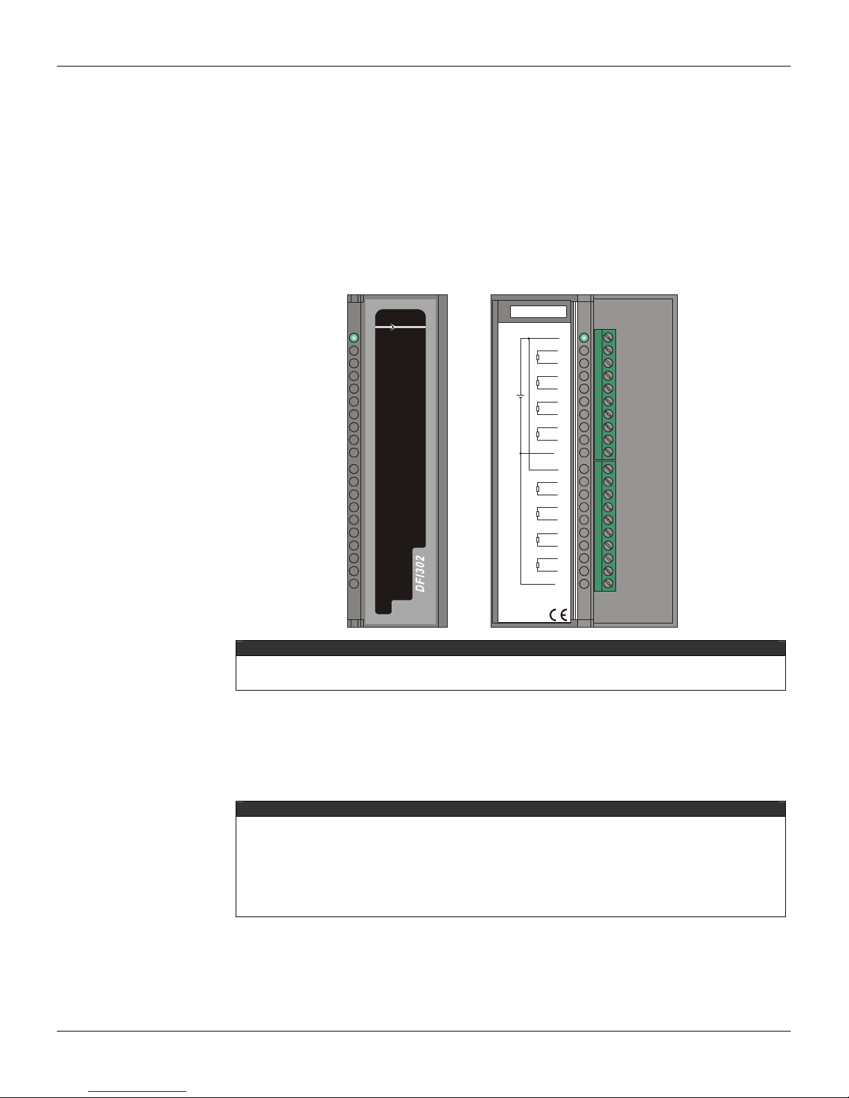
This module provides 4 pairs of analog outputs. Each pair is composed of one Current output and
one Voltage output. When one output is selected, the corresponding pair is selected simultaneously.
The current outputs can be configured individually on ranges 0-20 mA or 4-20 mA. For voltage
outputs the range is 0-5V, 1-5 V, ± 5 V, 0-10 V, 2-10 V or ± 10 V.
DF46
PWR
GND
PWR
GND
1A
+
2A
I 0
-
3A
+
4A
V0
-
5A
+
6A
I 1
-
7A
+
8A
V1
-
9A
10A
1B
+
2B
I 2
-
3B
+
4B
V2
-
5B
+
6B
I 3
-
7B
+
8B
V3
-
9B
10B
PWR
I 0
V0
I 1
V1
I 2
V2
I 3
V3
1 G 8x Temperature In
1 G 4x Analog Out
501/46 - 4 Analog Outputs 0-20mA, 4-20mA, 0-5V, 1-5V, 0-10V,±10V
smar
DipSwitche’s Configuration
When using Voltage Mode, make sure to configure the Group of Ranges via DipSwitches located
UP and Down inside the Box.
DipSwitch 1 - UP Side: Configure the Group of Ranges of Channel 0 (I0/V0)
DipSwitch 2 - UP Side: Configure the Group of Ranges of Channel 1 (I1/V1)
DipSwitch 1 - DOWN Side: Configure the Group of Ranges of Channel 2 (I2/V2)
DipSwitch 2 - DOWN Side: Configure the Group of Ranges of Channel 3 (I3/V3)
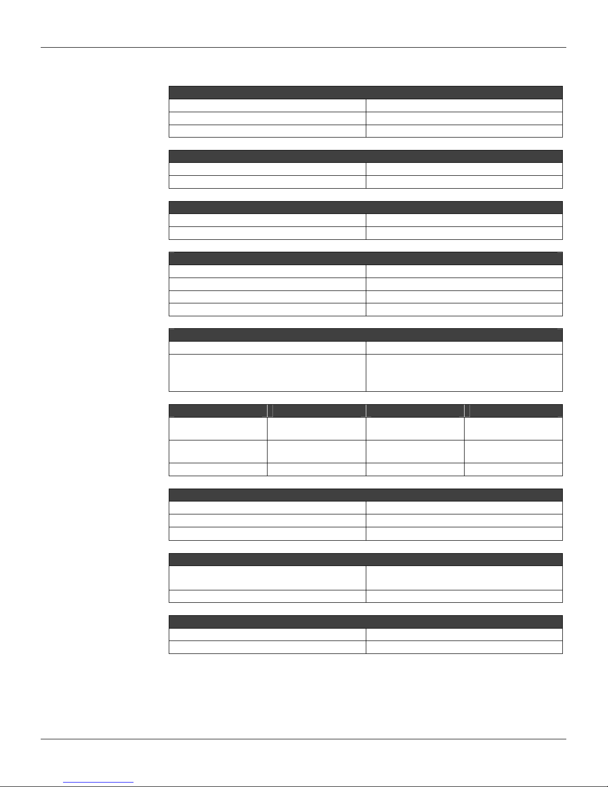
See under Technical Specifications (output range) the Group of Ranges.
Notes
In order to attend EMC standards, use shielded cables in signals inputs (ground the shield in the
panel only in one side of the cable) and cables less then 30 meters for power source inputs.
The scale for Analog Input and Output Modules is done using XD_SCALE parameter in AI and
AO blocks, respectively. When using MAI or MAO, it is assumed a default range, 4-20mA or 15V without possibility to change. For MAI and MAO, input and output parameters are available in
percentage of default range.
2
Page 5
Technical Speci fications
Num ber of Ou tputs 4
Number of Groups 1
Number of Points per Group 4
Channel To Bus Optical Isolation up to 3700 Vrms
Channel To External Supply 1500 Vac
Provided by the IMB bus 5 Vdc @ 20 mA Maximum
Total Maximum Dissipation 0.1 W
In Rush Current Consumption 2.3 A, 10ms @ 24 Vdc Maximum
Voltage Source 20 – 30 Vdc
Maximum Current 180 mA
Indicator of So urce Green LED
Outputs Type Single ended ( 1 ground)
Load Impedance
Out puts Range Range 1 Range 2 Range 3
Voltage Output Dip
Switch OFF
Voltage Output Dip
Switch ON
Current Output 4 mA to 20 mA 0 mA to 20 mA 0 mA to 20 mA
Conversion Speed 8 ms/channel
Resolution 12 bits
Accuracy at 77 °F (25 °C)
Dimensions (W x D x H)
Weight 0.330 kg
One wire 14 AWG (2 mm2)
Two wires 20 AWG (0.5 mm2)
DF46 – Installation M odule
Architecture
Isolation
Internal Power
External Power
Outputs
5 V: 2 kΩ minimum;
10 V: 5 kΩ minimu m
20 mA: 750 Ω maxi mu m
1 V to 5 V 0 V to 5 V -5 V to 5 V
2 V to 10 V 0 V to 10 V -10 V to 10 V
A/D Conversion
± 0.5% of span
Dimensions and Weight
39.9 x 137.0 x 141.5mm;
(1.57 x 5.39 x 5.57 in)
Cables
3
Page 6

DF46 – Installat ion M od ule
4
 Loading...