

SLS SL75232D, SL75232N Datasheet
SL75232
System Logic
Semiconductor
SLS
Line Driver / Receiver
Description
The SL75232N, SL75232D are monolithic device
containing 3 independent drives and 5 receivers. These are
designed to interface between date terminal equipment and
date communication equipment as designed by EIA-232-D.
Features
• Meets standard EIA-232-D (Revision of RS-232-C)
• Drivers
- Current Limited Output 10 mA Typical
- Power-off Output Impedance 300 Ω Min
- Slew Rate Control by Load Capacitor
- Flexible Supply Voltage Range
- Input Compatible with Most TTL and DTL Circuits
• Receivers
- Input Resistance 3 kΩ to 7 kΩ
- Input Signal Range ± 30 V
- Built -in Input Hysteresis (Double Threshold)
• 20 DIP/SO20: ÌS-001AD (SL75232N) / ÌS-013AÑ
(SL75232D)
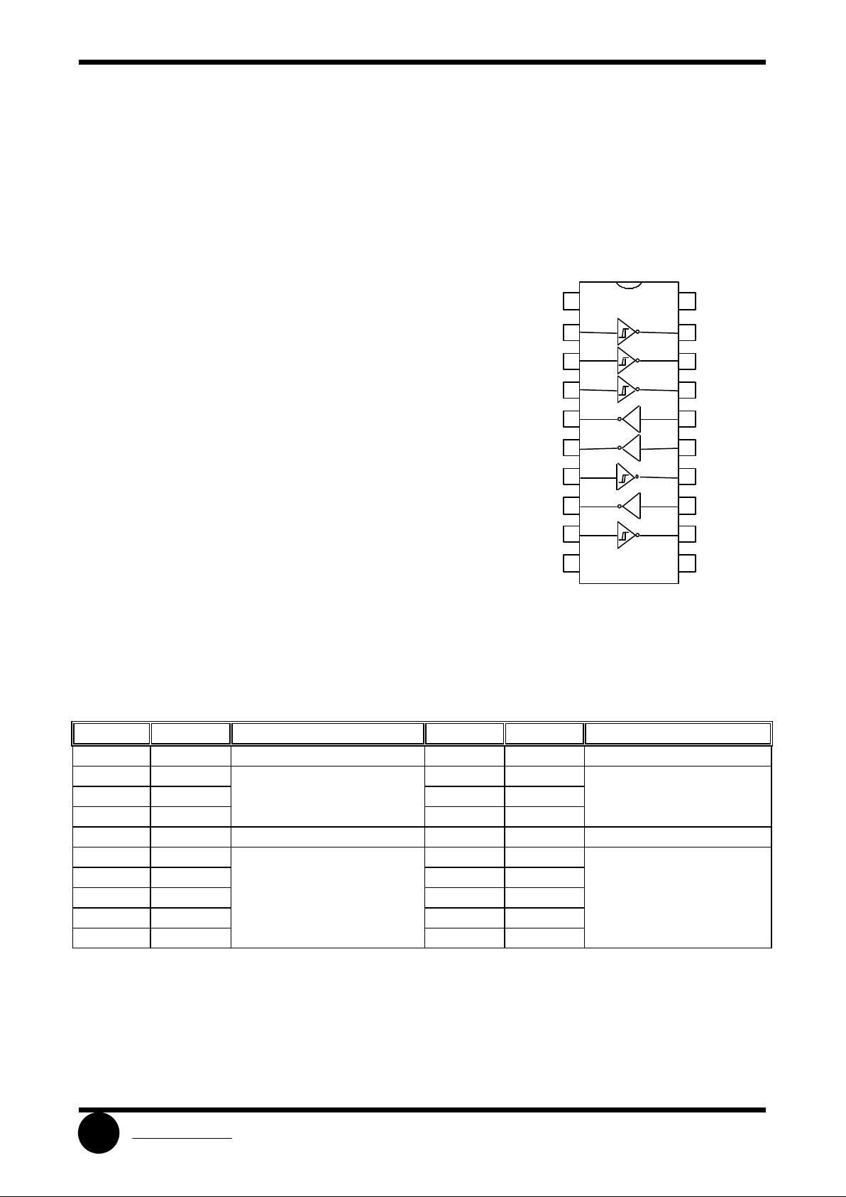
Pin Description
Name Pin No Function Name Pin No Function
V
CC+
1 Driver Section Supply + V
CC-
10 Driver Section Supply DA1 16 DY1 5
DA2 15 DY2 6 Driver Output
DA3 13 Driver Input DY3 8
VCC 20 Receiver Section Supply GND 11 Ground
RA1 2 RY1 19
RA2 3 RY2 18
RA3 4 Receiver Input RY3 17 Receiver Output
RA4 7 RY4 14
RA5 9 RY5 12
V
CC-
RA5
DY3
RA4
DY2
DY1
RA3
RA2
RA1
V
CC+
10
9
8
7
6
5
4
3
2
1
11
12
13
14
15
16
17
18
19
20
GND
RY5
DA3
RY4
DA2
DA1
RY3
RY2
RY1
V
CC
Block Diagram
IL75232N, IL75232D
SL75232
System Logic
Semiconductor SLS
Absolute Maximum Ratings
Symbol Parameter Rating Unit
V
CC+
Supply Voltage 15 V
V
CC-
Supply Voltage -15 V
VCC Supply Voltage 10 V
VI (Driver) Input Voltage
-15 ÷ +7
V
VI (Reciver) Input Voltage
± 30
V
VO (Driver) Output Voltage
-15 ÷ +15
V
PT Continuous Power Dissipation (Below 25 oC) 1.0 W
T
STG
Storage Temperature
-65 ÷ +175
o
C
Top Operating Temperature
0 ÷ +75
o
C
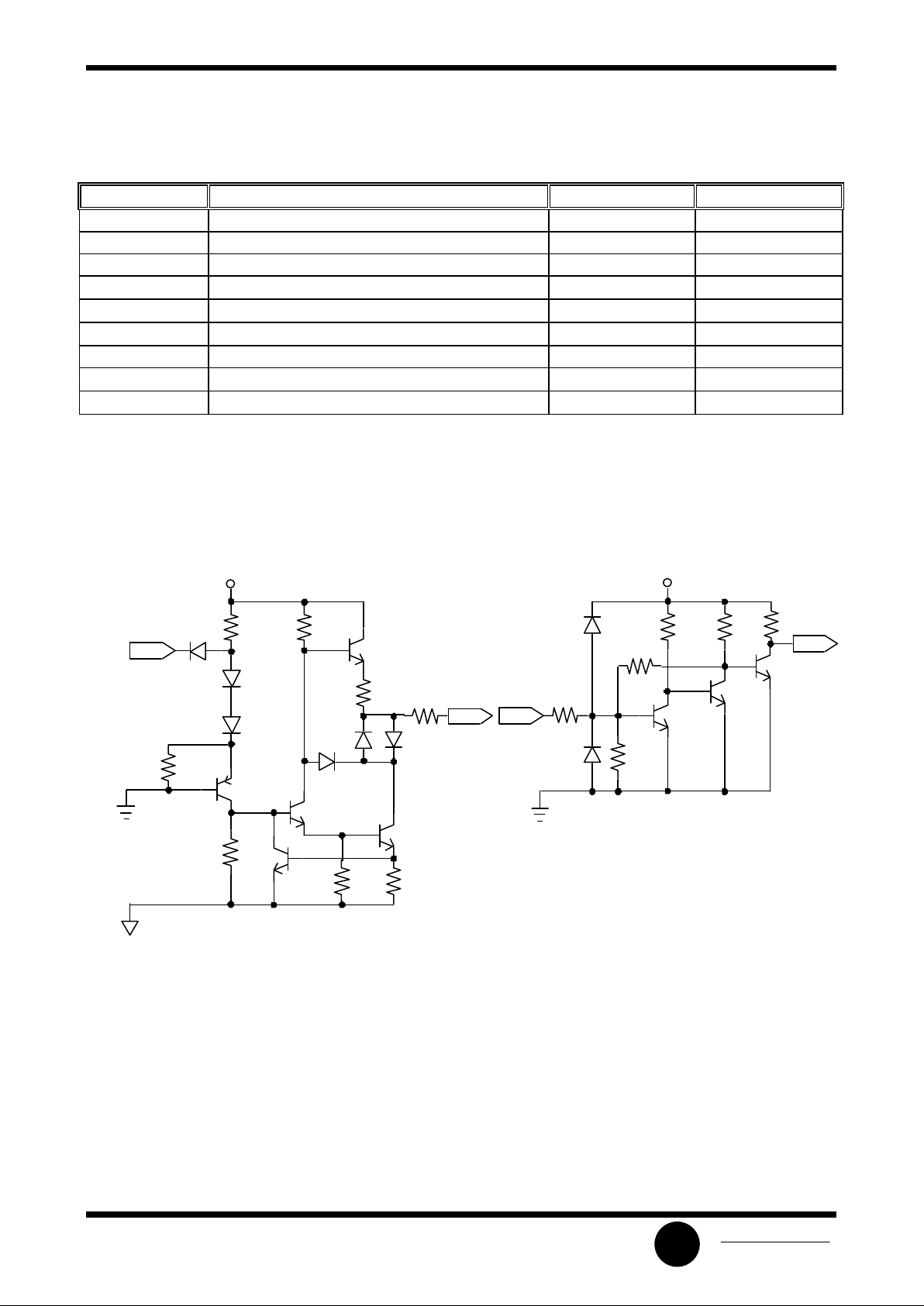
Schematic
V
CC-
300
70
6.2 Ê
8.2 Ê
70
7Ê
10Ê
3.6Ê
VCC+
DA
DY
DRIVER
RESEIVER
10 Ê
2 Ê
4 Ê
2 Ê
5 Ê9 Ê
V
CC
DA
DY
 Loading...