

SLS SL74LVU04, SL74LVU04D, SL74LVU04N Datasheet
TECHNICAL DATA
Semiconductor
1
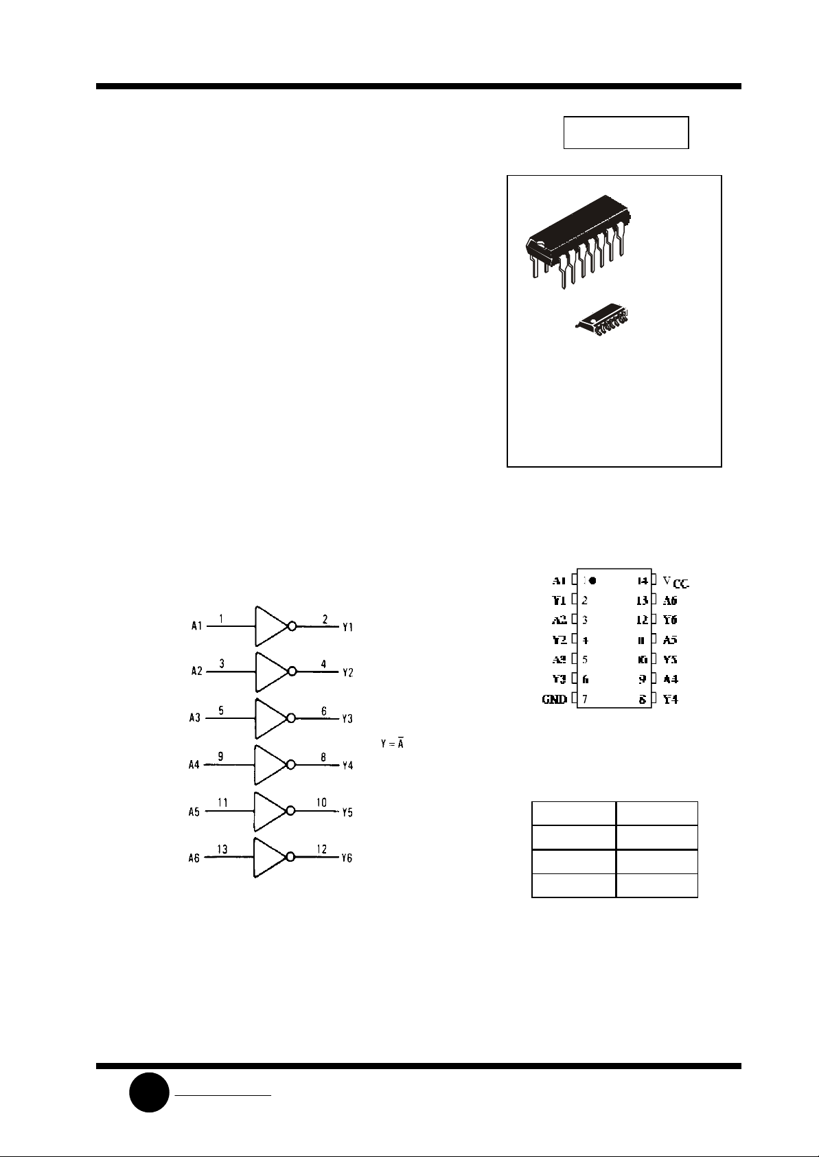
Hex Inverter
The 74LVU04 is a low -voltage, Si-gate CMOS device and is pin
compatible with the 74HCU04.
The 74LVU04 is a general purpose hex inverter. Each of the six
inverters is a single stage with unbuffered outputs.
• Wide Operating Voltage: 1.0÷5.5 V
• Optimized for Low Voltage applications: 1.0÷3.6 V
• Accepts TTL input levels between VCC =2.7 V and VCC =3.6 V
• Low Input Current
SL74LVU04
N SUFFIX
PLASTIC
14
1
14
ORDERING INFORMATION
SL74LVU04N Plastic
SL74LVU04D SOIC
SL74LVU04 Chip
TA = -40° ÷ 125° C for all packages
D SUFFIX
SOIC
LOGIC DIAGRAM
PIN 14 =VCC
PIN 7 = GND
PIN ASSIGNMENT
FUNCTION TABLE
Input Output
A Y
L H
H L
SLS
System Logic
1
SL74LVU04
Semiconductor
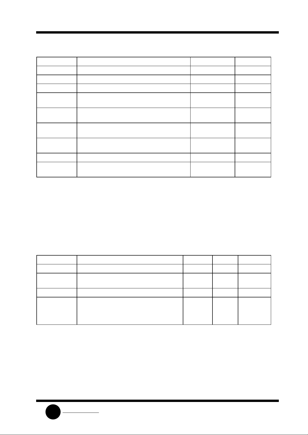
MAXIMUM RATINGS
*
Symbol Parameter Value Unit
VCC DC supply voltage (Referenced to GND) -0.5 ÷ +7.0 V
IIK *1 DC input diode current ±20 mA
IOK *2 DC output diode current ±50 mA
IO *3 DC output source or sink current
±25 mA
-bus driver outputs
ICC DC VCC current for types with
±50 mA
- bus driver outputs
I
DC GND current for types with
GND
±50 mA
- bus driver outputs
PD Power dissipation per package, plastic DIP+
SOIC package+
750
500
Tstg Storage temperature -65 ÷ +150 °C
TL Lead temperature, 1.5 mm from Case for 10 se conds
260 °C
(Plastic DIP ), 0.3 mm (SOIC Package)
*
Maximum Ratings are those values beyond which damage to the device may occur.
Functional operation should be restricted to the Recommended Operating Conditions.
+Derating - Plastic DIP: - 12 mW/°C from 70° to 125°C
SOIC Package: : - 8 mW/°C from 70° to 125°C
*1: VI < -0.5V or V
> VCC+0.5V
I
*2: Vo < -0.5V or Vo > VCC+0.5V
*3: -0.5V < Vo < VCC+0.5V
mW
RECOMMENDED OPERATING CONDITIONS
Symbol Parameter Min Max Unit
VCC DC Supply Voltage (Referenced to GND) 1.0 5.5 V
VIN, V
fields. However, precautions must be taken to avoid applications of any voltage higher than maximum rated voltages
to this high-impedance circuit. For proper operation, VIN and V
V
)≤VCC.
OUT
outputs must be left open.
DC Input Voltage, Output Voltage (Referenced
OUT
0 VCC V
to GND)
TA Operating Temperature, All Package Types -40 +125 °C
tr, tf Input Rise and Fall Time 1.0 V ≤VCC <2.0 V
2.0 V ≤VCC <2.7 V
2.7 V ≤VCC <3.6 V
3.6 V ≤VCC ≤5.5 V
0
0
0
0
500
200
100
50
ns
This device contains protection circuitry to guard against damage due to high static voltages or electric
should be constrained to the range GND≤(VIN or
OUT
Unused inputs must always be tied to an appropriate logic voltage level (e.g., either GND or VCC). Unused
SLS
System Logic
2
 Loading...