

SLS SL74LV573D, SL74LV573N Datasheet
SL74LV573
OCTAL D-TYPE TRANSPARENT LATCH (3-State)
By pinning SL74LV573 are compatible with SL74HC573 and
SL74HCT573 series. Input voltage levels are compatible with
stadard CMOS levels.
• Output voltage levels are compatible with input levels of CMOS,
NMOS and TTL ICS
• Voltage supply range from 1.2 to 5.5 V
• LOW input current: 1.0 µÀ; 0.1 µÀ at Ò = 25 °Ñ
• Output current 8 mÀ
• Latch current: not less than150 mÀ at Ò = 125 °Ñ
• ESD acceptable value: not less than 2000 V as per HBM and
not less than 200 V as per MM
FUNCTION TABLE
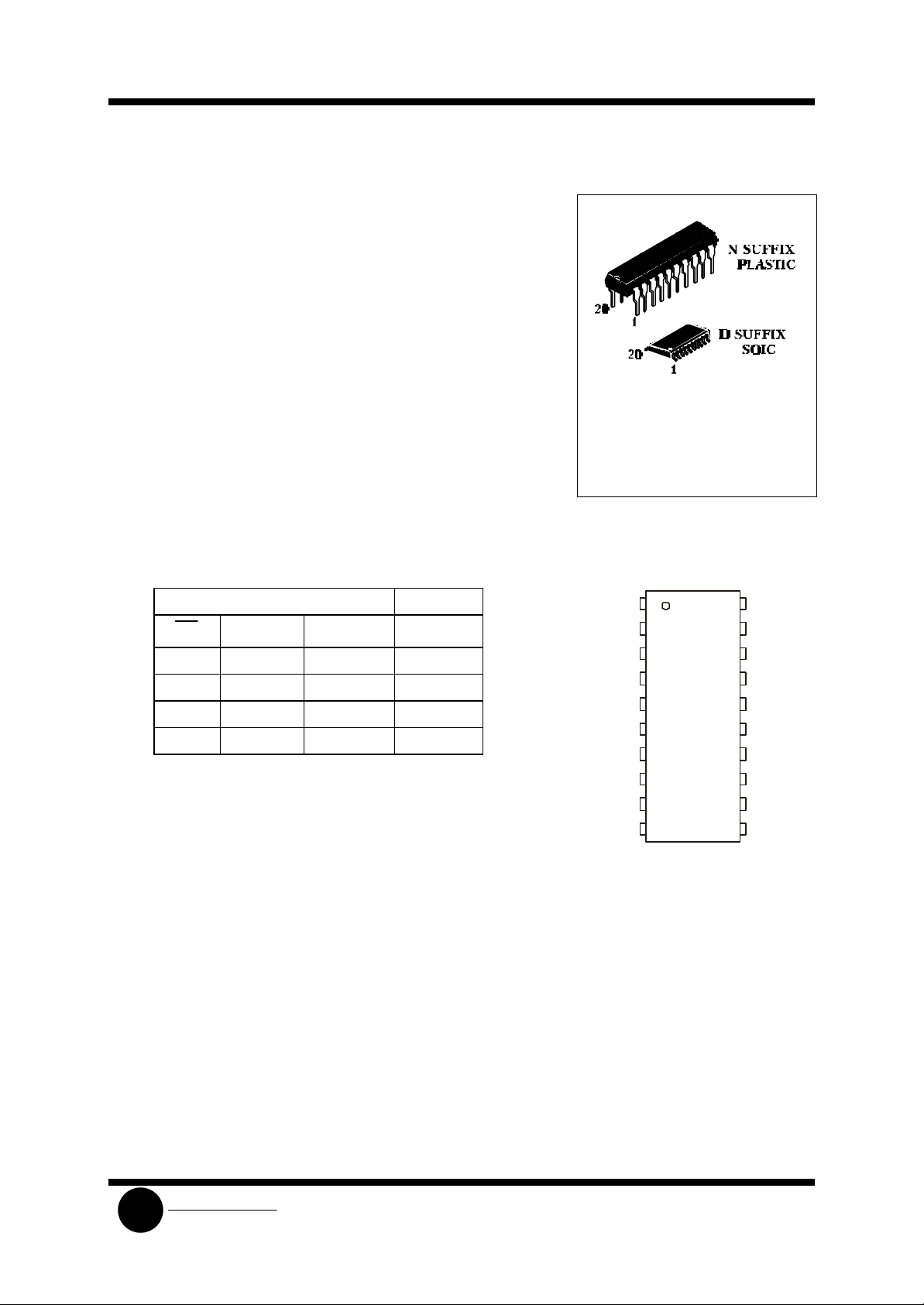
ORDERING INFORMATION
SL74LV573N Plastic DIP
SL74LV573D SOIC
TA = -40° to 125° C
for all packages
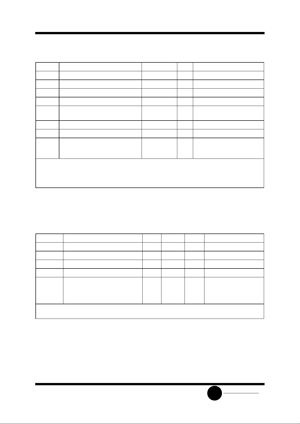
PIN ASSIGNMENT
Inputs Outputs
OE LE D Q
L H H H
L H L L
L L X no change
H X X Z
H -HIGH voltage level
L - LOW voltage level
X - don’t care
Z - High impedance state
OE
D0
D1
D2
D3
D4
D5
D6
D7
GND
1
2
3
4
5
6
7
8
9
10
20
19
18
17
16
15
14
13
12
11
V
Q0
Q1
Q2
Q3
Q4
Q5
Q6
Q7
LE
CC
System Logic
SLS
Semiconductor
SL74LV573
ABSOLUTE MAXIMUM RATINGS
Symbol Parameter Rating Unit Conditions
Vcc Supply voltage -0.5 to +7.0 V
Iik, Input diode current ±20 mA VI<-0.5 V or VI>Vcc>+0.5 V
Iok Output diode current ±50 mA V0<-0.5 V or VI>Vcc>+0.5 V
Io Output current bus drivers ±35 mA -0.5 V<Vo<Vcc+0.5 V
Icc DC Vcc or GND current for types
bus driver outputs
I
GND current ±50 mÀ
GND
Tstg Storage temperature range -65 to +150
PD Power dissipation per package:
DIP
SO
Notes:
Power dissipation value decreases for:
DIP - 12 mW°C the range from 70 to 125°Ñ
SO - 8 mW°C the range from 70 to 125°Ñ
±70
750
500
mA
î
Ñ
mW
RECOMMENDED OPERATING CONDITIONS
Symbol Parameter Min Max Unit Conditions
Vcc Supply voltage 1.0 5.5 V
VI Input voltage 0 Vcc V
Vî Output voltage 0 Vcc V
T Operating temperature range -40 +125
tr,tf Input rise and fall times 500
200
100
50
Note - The IC function down to Vññ = 1.0 V (input levels - VIL=0 V, VIH=Vcc); DC characterisics are
guaranteed at Vcc=1.2 ÷ 5.5 V.
o
C
ns/V Vcc= 1.0 ÷ 2.0 V
Vcc= 2.0 ÷ 2.7 V
Vcc= 2.7 ÷ 3.6 V
Vcc= 3.6 ÷ 5.5 V
System Logic
SLS
Semiconductor
 Loading...