

SLS SL74LV245D, SL74LV245N Datasheet
SL74LV245
Semiconductor
OCTAL BUS TRANSCEIVER (3-State)
By pinning SL74LV245 are compatible with SL74HC245 and SL74HCT245 series. Input voltage levels
are compat ible with standard CMOS levels.
• Output voltage levels are compatible with input levels of CMOS,
NMOS and TTL ICS
• Supply voltage range: 2.0 to 3.2 V
• Low input current: 1.0 µÀ; 0.1 µÀ at Ò = 25 °Ñ
• Output current 8 mÀ
• Latch current value: not less 150 mÀ at Ò = 125 °Ñ
• ESD acceptable values: not less than 2000 V as per HBM and
not less 200 V as per ÌÌ
•
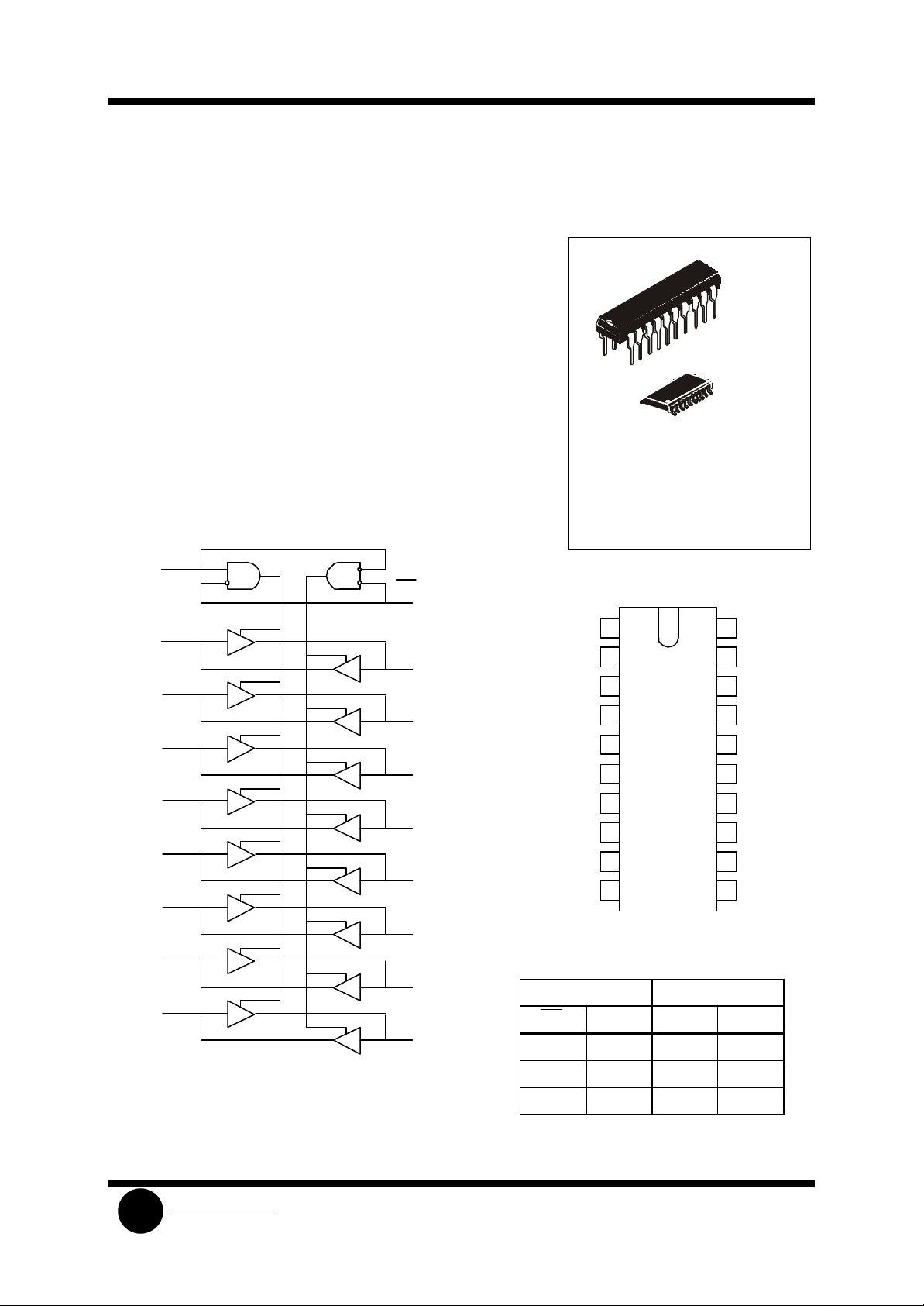
BLOCK DIAGRAM
20
1
20
ORDERING INFORMATION
SL74LV245N Plastic DIP
SL74LV245D SOIC
TA = -40° to 125° C
for all packages
N SUFFIX
PLASTIC
D SUFFIX
SOIC
1
DIR
01
OE
PIN ASSIGNMENT
19
02
03
04
05
06
07
08
09
A
0
B
0
A
1
A
2
A
3
A
4
A
5
A
6
A
7
18
B
1
17
B
2
16
B
3
15
B
4
14
B
5
13
B
6
12
B
7
11
Pin 20=VCC
Pin 10 = GND
DIR 01
A
02
0
A
03
1
A
04
2
A
05
GND
3
A
06
4
A
07
5
A
08
6
A
09
7
10
245
FUNCTION TABLE
Inputs Inputs/Outputs
OE DIR À Â
L L A=B input
L H input B=A
H X Z Z
20
V
CC
OE
19
B
18
0
B
17
1
B
16
2
15
B
3
B
14
4
B
13
5
B
12
6
B
11
7
SLS
System Logic
SL74LV245
Semiconductor
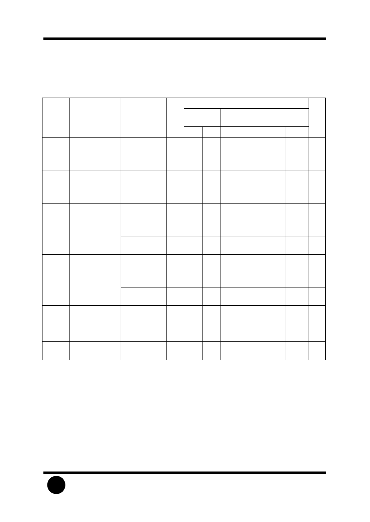
ABSOLUTE MAXIMUM RATINGS*
Symbol Parameter Rating Unit
VCC Supply voltage -0.5 to +5.0 V
IIK *1 Input diode current ±20 mÀ
IOK *2 Output diode current ±50 mÀ
IO *3 Output source or sink current ±35 mÀ
ICC VCC current ±70 mÀ
I
GND current ±70 mÀ
GND
PD Power dissipation per package:
Plastic DIP *4
SOIC *4
Tstg Storage temperature range -65 to +150 °C
*
In absolute max imum ratings modes functioning is not guaranteed. Vpon lifting the absolute
maximum ratings functioning is guaranteed at the recommended operating conditions.
*1 Provided VI < -0.5 V or VI > VCC + 0.5 V.
*2 Provided VO < -0.5 V or VO > VCC + 0.5 V.
*3 Provided -0.5 V < VO < VCC + 0.5 V.
*4 When operating in the temperature range of 70°Ñ to 125°C power dissipation value decreases:
- for Plastic DIP by 12 mW/°C
- for SOIC by 8 mW/°C
750
500
mW
RECOMMENDED OPERATING CONDITIONS
Symbol Parameter Min Max Unit
VCC Supply voltage 1.2 3.6 V
VIN Input voltage 0 VCC V
V
Output voltage 0 VCC V
OUT
TA Operating ambient temperature range. For all
package types
tLH, tHL Input rise and fall times VCC =1.2 V
VCC =2.0 V
VCC =3.0 V
V
=3.6 V
CC
-40 125 °C
0 1000
700
500
400
ns
SLS
System Logic
SL74LV245
Semiconductor
DC CHARACTERISTICS
Test VCC, Limits
Symbol Parameter conditions V 25°C -40°C to
85°C
min max min max min max
VIH HIGH level input
voltage
VIL LOW level output
voltage
VOH HIGH level output
voltage
VI = VIH or VIL
VOL LOW level output
voltage
VI = VIH or VIL
VO = VCC-0.1 V 1.2
2.0
3.0
3.6
VO =0.1 V 1.2
2.0
3.0
3.6
VI = VIH or VIL
IO = -50 µÀ
IO = -8 mÀ
VI = VIH or VIL
IO = 50 µÀ
IO = 8 mÀ
1.2
2.0
3.0
3.6
3.0 2.48 - 2.34 - 2.20 - V
1.2
2.0
3.0
3.6
3.0 - 0.33 - 0.4 - 0.5 V
0.9
1.4
2.1
2.5
-
-
-
-
1.1
1.92
2.92
3.52
-
-
-
-
-
-
-
-
0.3
0.6
0.9
1.1
-
-
-
-
0.09
0.09
0.09
0.09
0.9
1.4
2.1
2.5
-
-
-
-
1.0
1.9
2.9
3.5
-
-
-
-
-
-
-
-
0.3
0.6
0.9
1.1
-
-
-
-
0.1
0.1
0.1
0.09
125°C Unit
0.9
1.4
2.1
2.5
-
-
-
-
1.0
1.9
2.9
3.5
-
-
-
-
-
-
-
-
0.3
0.6
0.9
1.1
-
-
-
-
0.1
0.1
0.1
0.09
V
V
V
V
II Input current VI = VCC or 0 V 3.6 - ±0.1 - ±1.0 - ±1.0 µÀ
IOZ OFF-state current 3-state outputs
VI = V
VO =VCC or 0 V
ICC Supply current VI =VCC or 0 V
IO = 0 µÀ
System Logic
SLS
IL
or V
3.6 - ±0.5 - ±5 - ±10 µÀ
IH
3.6 - 8.0 - 80 - 160 µÀ
 Loading...