

SLS SL74LS244D, SL74LS244N Datasheet
Semiconductor
Octal 3-State Noninverting Buffer/Line
Driver/Line Receiver
These octal buffers and line drivers and designed specifically to
improve both the performance and density of three-state memory
address drivers, clock drivers, and busoriented receivers and
transmitters.
This devise features high fan-out, improved fan-in, and 400 mV noise
margin.
It can be used to drive terminated lines down to 133 ohms.
• 3-State Outputs Drive Bus Lines or Buffer Memory Address
Registers
• P-N-P Inputs Reduce D-C Loading
• Hysteresis at Inputs Improves Noise Margins
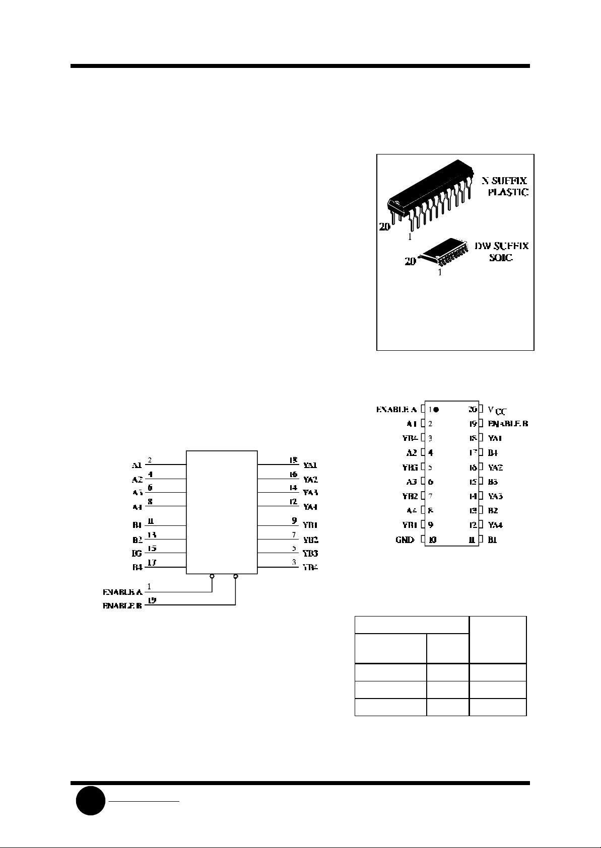
ORDERING INFORMATION
SL74LS244N Plastic
SL74LS244D SOIC
SL74LS244
TA = 0° to 70° C
for all packages
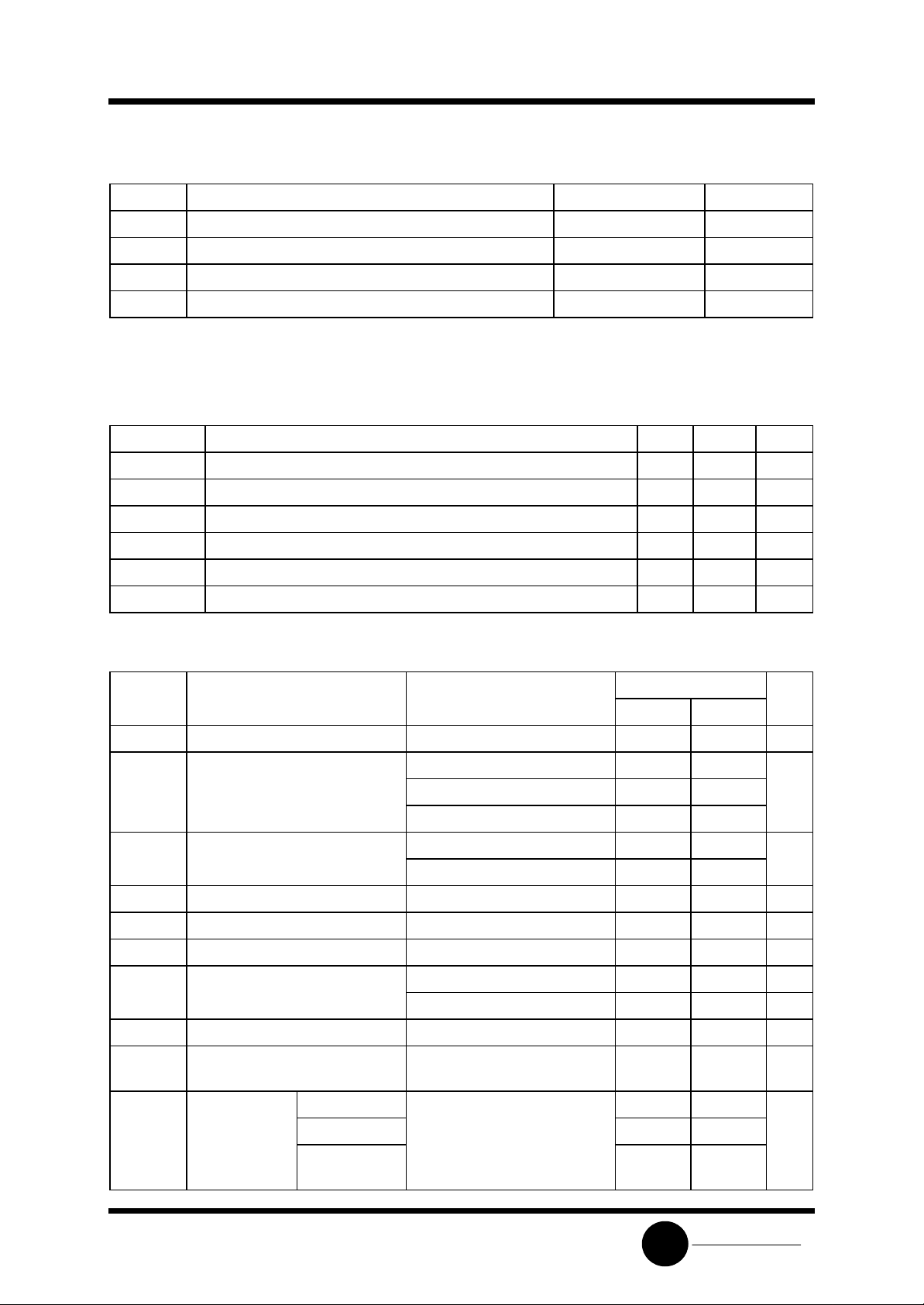
LOGIC DIAGRAM
PIN 20=VCC
PIN 10 = GND
PIN ASSIGNMENT
FUNCTION TABLE
Inputs Outputs
Enable A,
Enable B
L L L
L H H
A,B YA,YB
SLS
H X Z
X=don’t care
Z = high impedance
System Logic
SL74LS244
Semiconductor
MAXIMUM RATINGS*
Symbol Parameter Value Unit
VCC Supply Voltage 7.0 V
VIN Input Voltage 7.0 V
V
Output Voltage 5.5 V
OUT
Tstg Storage Temperature Range -65 to +150 °C
*
Maximum Ratings are those values beyond which damage to the device may occur.
Functional operation should be restricted to the Recommended Operating Conditions.
RECOMMENDED OPERATING CONDITIONS
Symbol Parameter Min Max Unit
VCC Supply Voltage 4.75 5.25 V
VIH High Level Input Voltage 2.0 V
VIL Low Level Input Voltage 0.8 V
IOH High Level Output Current -15 mA
IOL Low Level Output Current 24 mA
TA Ambient Temperature Range 0 +70 °C
DC ELECTRICAL CHARACTERISTICS over full operating conditions
Guaranteed Limit
Symbol Parameter Test Conditions Min Max Unit
VIK Input Clamp Voltage VCC = min, IIN = -18 mA -1.5 V
VOH High Level Output Voltage VCC = min, IOH = -1.0 mA 2.7 V
VCC = min, IOH = -3.0 mA 2.4
VCC = min, IOH = -15 mA 2.0
VOL Low Level Output Voltage VCC = min, IOL = 12 mA 0.4 V
VCC = min, IOL = 24 mA 0.5
VT+ - VT- Hysteresis VCC = min 0.2 V
I
Output Off Current HIGH VCC = max, V
OZH
I
Output Off Current LOW VCC = max, V
OZL
IIH High Level Input Current VCC = max, VIN = 2.7 V 20 µA
= 2.7 V 20 µA
OUT
= 0.4 V -20 µA
OUT
VCC = max, VIN = 7.0 V 0.1 mA
IIL Low Level Input Current VCC = max, VIN = 0.4 V -0.2 mA
IO Output Short Circuit Current VCC = max, VO =0 V
-40 -225 mA
(Note 1)
ICC Supply Outputs High VCC = max 27 mA
Current Outputs Low Outputs open 46
All outputs
54
disabled
System Logic
SLS
 Loading...