

SLS SL74LS164D, SL74LS164N Datasheet
Semiconductor
8-Bit Serial-Input/Parallel-Output
SL74LS164
Shift Register
This 8-bit shift register features gated serial inputs and an
asynchronous reset. The gated serial inputs (A and B) permit complete
control over incoming data as a low at either (or both) input(s) inhibits
entry of the new data and resets the first flip flop to the low level at the
next clock pulse. A high level input enables the other input which will
then determine the state of the first flip -flop. Data at the serial inputs
may be changed while the clock is high or low, but only information
meeting the setup requirements will be entered clocking occurs or the
low-to-high level transition of the clock input. All inputs are diodeclamped to minimize transmission-line effects.
• Gated (Enable/Disable) Serial Inputs
• Fully Buffered Clock and Serial Inputs
• Asynchronous Clear
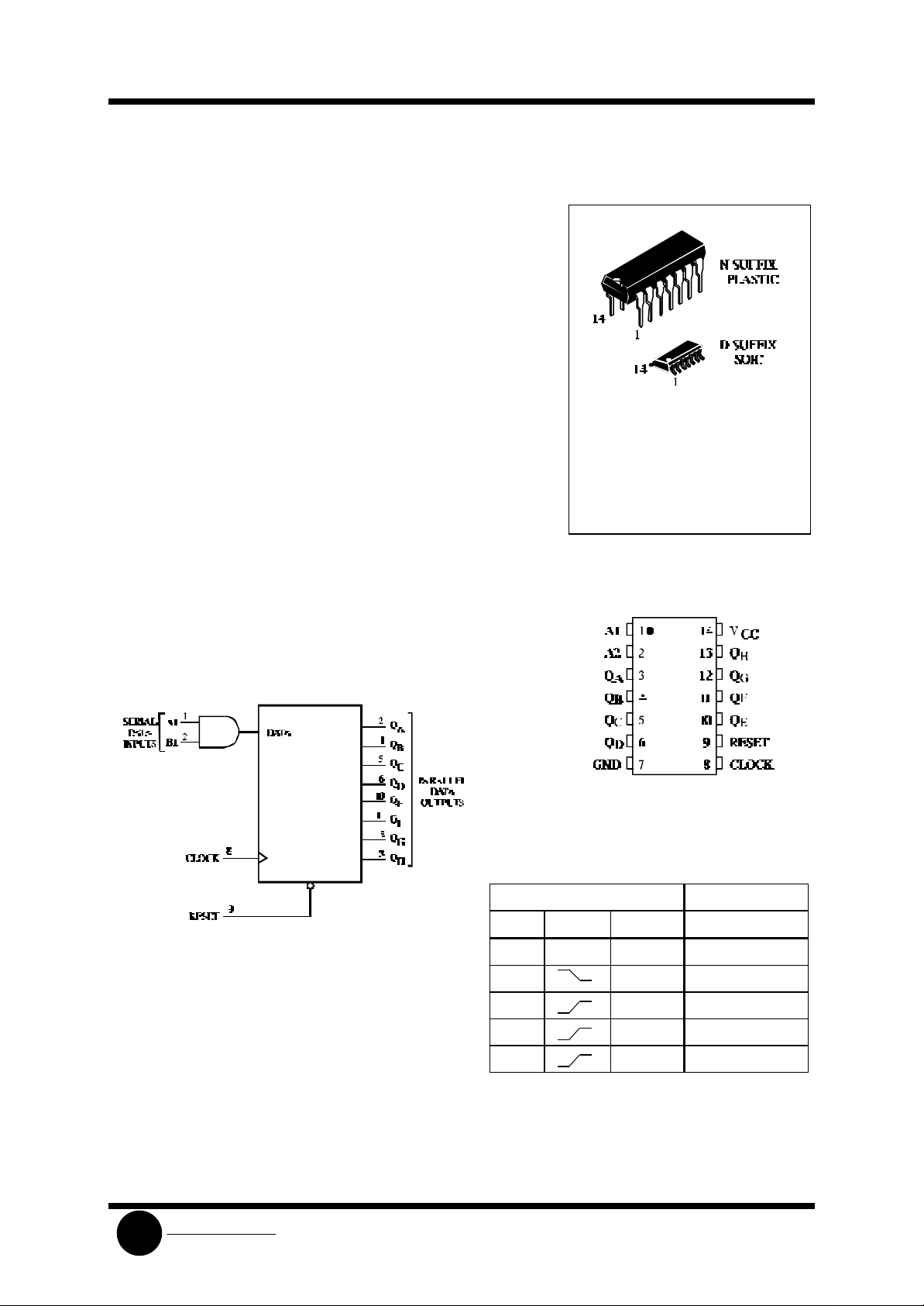
LOGIC DIAGRAM
ORDERING INFORMATION
SL74LS164N Plastic
SL74LS164D SOIC
TA =0° to 70°C
for all packages
PIN ASSIGNMENT
PIN 14 =VCC
PIN 7 = GND
FUNCTION TABLE
Inputs Outputs
Reset Clock A1 A2 QA QB ... QH
L X X X L L ... L
H X X no change
H H D D QAn ... QGn
H D H D QAn ... QGn
H L L L QAn ... QGn
D = data input
X = don’t care
QAn - Q
rising edge at the clock input.
= data shifted from the previous stage on a
Gn
SLS
System Logic
SL74LS164
Semiconductor
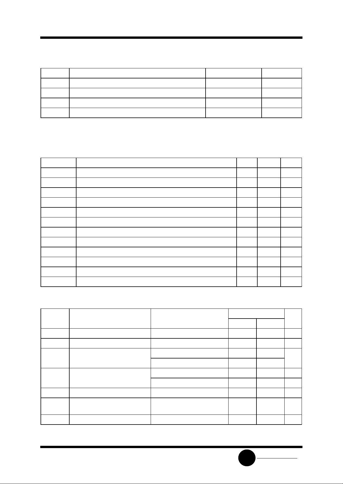
MAXIMUM RATINGS*
Symbol Parameter Value Unit
VCC Supply Voltage 7.0 V
VIN Input Voltage 7.0 V
V
Output Voltage 5.5 V
OUT
Tstg Storage Temperature Range -65 to +150 °C
*
Maximum Ratings are those values beyond which damage to the device may occur.
Functional operation should be restricted to the Recommended Operating Conditions.
RECOMMENDED OPERATING CONDITIONS
Symbol Parameter Min Max Unit
VCC Supply Voltage 4.75 5.25 V
VIH High Level Input Voltage 2.0 V
VIL Low Level Input Voltage 0.8 V
IOH High Level Output Current -0.4 mA
IOL Low Level Output Current 8.0 mA
TA Ambient Temperature Range 0 +70 °C
f
Clock Frequency 0 25 MHz
clock
tsu Setup Time, A1 or A2 to Clock 15 ns
th Hold Time, Clock to A1 or A2 5 ns
tw Pulse Width, Clock 20 ns
tw Pulse Width, Reset 20 ns
t
Recovery Time 5 ns
rec
DC ELECTRICAL CHARACTERISTICS over full operating conditions
Guaranteed Limit
Symbol Parameter Test Conditions Min Max Unit
VIK Input Clamp Voltage VCC = min, IIN = -18 mA -1.5 V
VOH High Level Output Voltage VCC = min, IOH = -0.4 mA 2.7 V
VOL Low Level Output Voltage VCC = min, IOL = 4 mA 0.4 V
VCC = min, IOL = 8 mA 0.5
IIH High Level Input Current VCC = max, VIN = 2.7 V 20 mA
VCC = max, VIN = 7.0 V 0.1 mA
IIL Low Level Input Current VCC = max, VIN = 0.4 V -0.4 mA
IO Output Short Circuit Current VCC = max, VO = 0 V
(Noote 1)
ICC Supply Current VCC = max (Note 2) 27 mA
Note 1: Not more than one output should be shorted at a time, and duration should not exceed one second.
-20 -100 mA
System Logic
SLS
 Loading...