

SLS SL74HC299D, SL74HC299N Datasheet
Semiconductor
8-Bit Bidirectional Universal
Shift Register with Parallel I/O
High-Performance Silicon-Gate CMOS
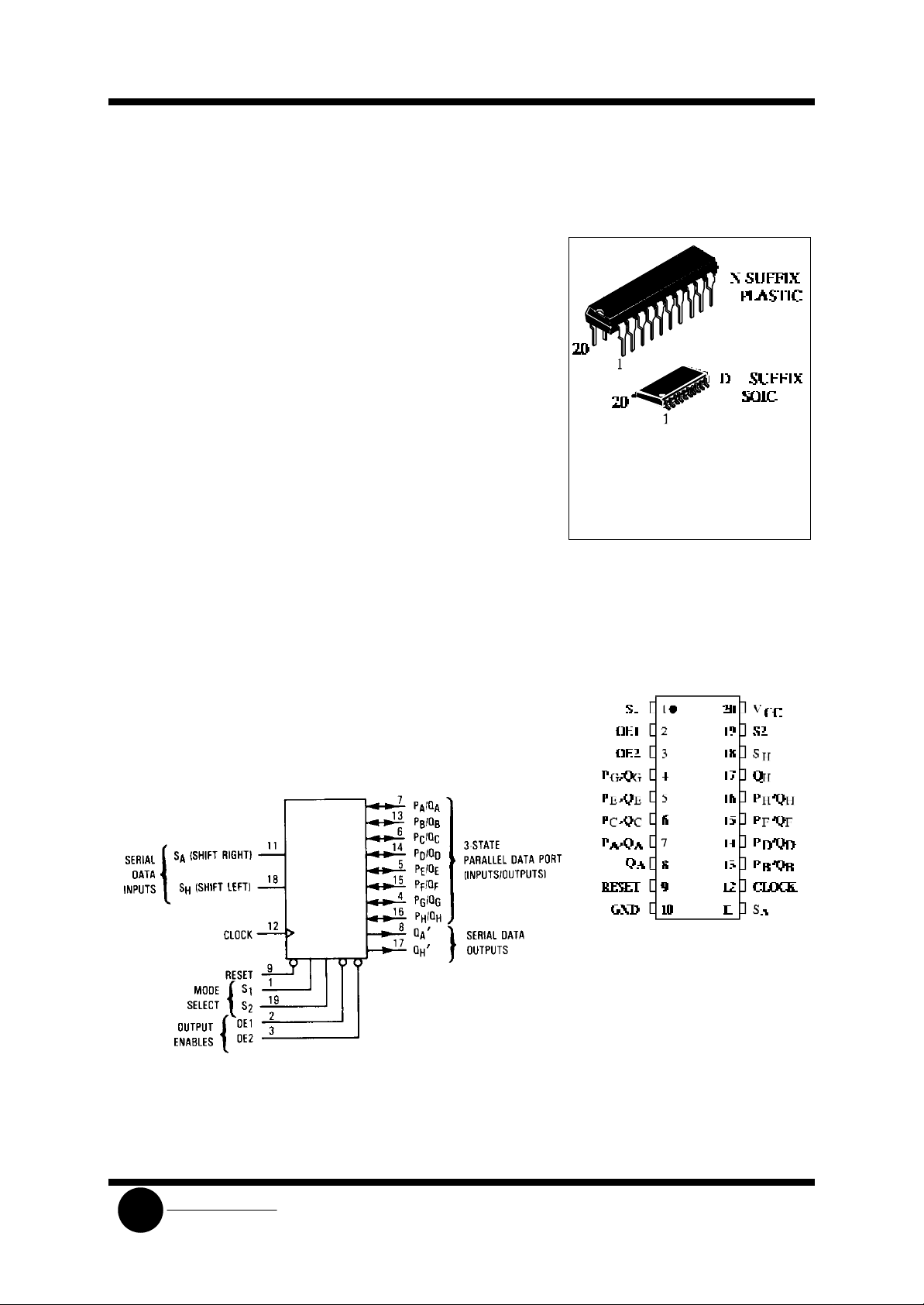
The SL74HC299 is identical in pinout to the LS/ALS299. The device
inputs are compatible with standard CMOS outputs; with pullup
resistors, they are compatible with LS/ALSTTL outputs.
The SL74HC299 features a multiplexed parallel input/output data
port to achieve full 8-bit handling in a 20 pin package. Due to the large
output drive capability and the 3-state feature, this device is ideally
suited for interface with bus lines in a bus-oriented system.
Two Mode-Select inputs and two Output Enable inputs are used to
choose the mode of operation as listed in the Function Table.
Synchronous parallel loading is accomplished by taking both ModeSelect lines, S1 and S2, high. This places the outputs in the highimpedance state, which permits data applied to the data port to be
clocked into the register. Reading out of the register can be
accomplished when the outputs are enabled. The active-low
asynchronous Reset overrides all other inputs.
• Outputs Directly Interface to CMOS, NMOS, and TTL
• Operating Voltage Range: 2.0 to 6.0 V
• Low Input Current: 1.0 µA
• High Noise Immunity Characteristic of CMOS Devices
SL74HC299
ORDERING INFORMATION
SL74HC299N Plastic
SL74HC299D SOIC
TA = -55° to 125° C for all packages
PIN ASSIGNMENT
LOGIC DIAGRAM
PIN 20=VCC
PIN 10 = GND
SLS
System Logic
SL74HC299
Semiconductor
MAXIMUM RATINGS*
Symbol Parameter Value Unit
VCC DC Supply Voltage (Referenced to GND) -0.5 to +7.0 V
VIN DC Input Voltage (Referenced to GND) -1.5 to VCC +1.5 V
V
DC Output Voltage (Referenced to GND) -0.5 to VCC +0.5 V
OUT
IIN DC Input Current, per Pin ±20 mA
I
DC Output Current, per Pin ±35 mA
OUT
ICC DC Supply Current, VCC and GND Pins ±75 mA
PD Power Dissipation in Still Ai r, Plastic DIP+
SOIC Package+
750
500
Tstg Storage Temperature -65 to +150 °C
TL Lead Temperature, 1 mm from Case for 10 Seconds
260 °C
(Plastic DIP or SOIC Package)
*
Maximum Ratings are those values beyond whi ch damage to the device may occur.
Functional operation should be restricted to the Recommended Operating Conditions.
+Derating - Plastic DIP: - 10 mW/°C from 65° to 125°C
SOIC Package: : - 7 mW/°C from 65° to 125°C
RECOMMENDED OPERATING CONDITIONS
Symbol Parameter Min Max Unit
VCC DC Supply Voltage (Referenced to GND) 2.0 6.0 V
VIN, V
DC Input Voltage, Output Voltage (Referenced to GND) 0 VCC V
OUT
TA Operating Temperature, All Package Types -55 +125 °C
tr, tf Input Rise and Fall Time (Figure 1) VCC =2.0 V
VCC =4.5 V
V
=6.0 V
CC
0
1000
0
0
500
400
mW
ns
This device contains protection circuitry to guard against damage due to high static voltages or electric
fields. However, precautions must be taken to avoid applications of any voltage higher than maximum rated
voltages to this high-impedance circuit. For proper operation, VIN and V
GND≤(VIN or V
OUT
)≤VCC.
should be constrained to the range
OUT
Unused inputs must always be tied to an appropriate logic voltage level (e.g., either GND or VCC).
Unused outputs must be left open. I/O pins must be connected to a properly terminated line or bus.
System Logic
SLS
SL74HC299
Semiconductor
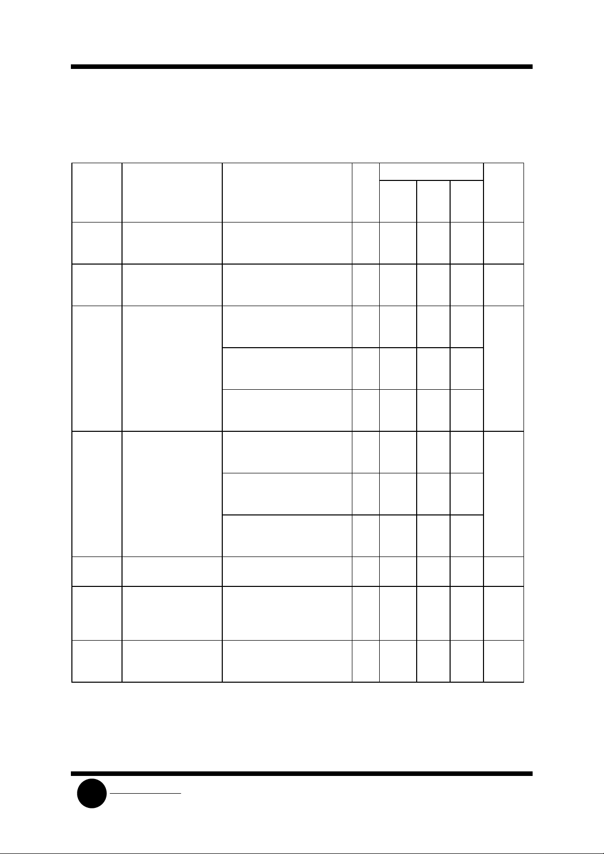
DC ELECTRICAL CHARACTERISTICS(Voltages Referenced to GND)
VCC Guaranteed Limit
Symbol Parameter Test Conditions V 25 °C
to
-55°C
VIH Minimum High-Level
Input Voltage
VIL Maximum Low -Level
Input Voltage
VOH Minimum High-Level
Output Voltage
VIN=VIH or VIL
VIN=VIH or VIL
VOL Maximum Low -Level
Output Voltage
VIN=VIH or VIL
VIN=VIH or VIL
IIN Maximum Input
V
=0.1 V or VCC-0.1 V
OUT
I
≤ 20 µA
OUT
V
=0.1 V or VCC-0.1 V
OUT
I
≤ 20 µA
OUT
VIN=VIH or VIL
I
≤ 20 µA
OUT
I
≤ 6.0 mA (P/Q)
OUT
I
≤ 7.8 mA (P/Q)
OUT
I
≤ 4.0 mA (Q’)
OUT
I
≤ 5.2 mA (Q’)
OUT
VIN= VIL or VIH
I
≤ 20 µA
OUT
I
≤ 6.0 mA (P/Q)
OUT
I
≤ 7.8 mA (P/Q)
OUT
I
≤ 4.0 mA (Q’)
OUT
I
≤ 5.2 mA (Q’)
OUT
2.0
4.5
6.0
2.0
4.5
6.0
2.0
4.5
6.0
4.5
6.0
4.5
6.0
2.0
4.5
6.0
4.5
6.0
4.5
6.0
1.5
3.15
4.2
0.3
0.9
1.2
1.9
4.4
5.9
3.98
5.48
3.98
5.48
0.1
0.1
0.1
0.26
0.26
0.26
0.26
VIN=VCC or GND 6.0 ±0.1 ±1.0 ±1.0 µA
Leakage Current
≤85
°C
1.5
3.15
4.2
0.3
0.9
1.2
1.9
4.4
5.9
3.84
5.34
3.84
5.34
0.1
0.1
0.1
0.33
0.33
0.33
0.33
≤125
°C
1.5
3.15
4.2
0.3
0.9
1.2
1.9
4.4
5.9
3.7
5.2
3.7
5.2
0.1
0.1
0.1
0.4
0.4
0.4
0.4
Unit
V
V
V
V
IOZ Maximum Three-State
Leakage Current
(QA thru QH)
ICC Maximum Quiescent
Supply Current
(per Package)
System Logic
SLS
Output in High-Impedance
State
VIN= V
V
IL
OUT=VCC
or V
IH
or GND
VIN=VCC or GND
I
=0µA
OUT
6.0 ±0.5 ±5.0 ±10 µA
6.0 8.0 80 160 µA
 Loading...