

SLS SL74HC221D, SL74HC221N Datasheet
Semiconductor
Dual Monostable Multivibrator
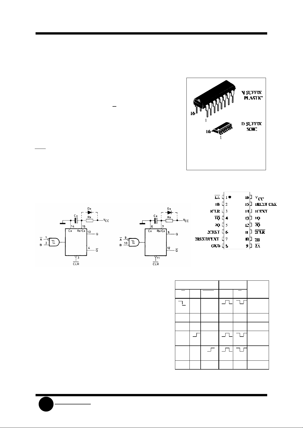
The SL74HC221 is identical in pinout to the LS/ALS221. The device
inputs are compatible with standard CMOS outputs; with pullup
resistors, they are compatible with LS/ALSTTL outputs.
There are two trigger inputs, A INPUT (negative edge) and
B INPUT (positive edge). These inputs are valid for rising/falling
signals
The device may also be triggered by using the CLR input (positiveedge) because of the Schmitt-trigger input; after triggering the output
maintains the MONOSTABLE state for the time period determined by
the external resistor RX and capacitor CX. Taking CLR low breaks this
MONOSTABLE STATE. If the next trigger pulse occurs during the
MONOSTABLE period it makes the MONOSTABLE period longer.
• Outputs Directly Interface to CMOS, NMOS, and TTL
• Operating Voltage Range: 3.0 to 6.0 V
• Low Input Current: 1.0 µA
• High Noise Immunity Characteristic of CMOS Devices
SL74HC221
ORDERING INFORMATION
SL74HC221N Plastic
SL74HC221D SOIC
TA = -55° to 125° C for all packages
PIN ASSIGNMENT
LOGIC DIAGRAM
PIN 16 =VCC
PIN 8 = GND
Note
(1) CX, RX, DX are external components.
(2) DX is a clamping diode.
The external capacitor is charged to VCC in the stand-by
state, i.e. no trigger. When the supply voltage is turned off
CX is discharged mainly through an internal parasitic diode.
If CX is sufficiently large and VCC decreases rapidy, there will
be some possibility of damaging the I.C. with a surge
current or latch-up. If the voltage supply filter capacitor is
large enough and VCC decrease slowly, the surge current is
automatically limited and damage the I.C. is avoided. The
maximum forward current of the parasitic diode is
approximately 20 mA.
FUNCTION TABLE
Inputs Outputs Note
A B CLR Q Q
H H Output
X L H L * H * Inhibit
H X H L * H * Inhibit
L H Output
L H Output
X X L L H Inhibit
X = don’t care
*
- except for monostable period
Enable
Enable
Enable
SLS
System Logic
SL74HC221
Semiconductor
MAXIMUM RATINGS*
Symbol Parameter Value Unit
VCC DC Supply Voltage (Referenced to GND) -0.5 to +7.0 V
VIN DC Input Voltage (Referenced to GND) -1.5 to VCC +1.5 V
V
DC Output Voltage (Referenced to GND) -0.5 to VCC +0.5 V
OUT
IIN DC Input Current, per Pin A, B, CLR
CX, RX
I
DC Output Current, per Pin ±25 mA
OUT
ICC DC Supply Current, VCC and GND Pins ±50 mA
±20
±30
mA
PD Power Dissipation in Still Air, Plastic DIP+
SOIC Package+
750
500
Tstg Storage Temperature -65 to +150 °C
TL Lead Temperature, 1 mm from Case for 10 Seconds
260 °C
(Plastic DIP or SOIC Package)
*
Maximum Ratings are those values beyond which damage to the device may occur.
Functional operation should be restricted to the Recommended Operating Conditions.
+Derating - Plastic DIP: - 10 mW/°C from 65° to 125°C
SOIC Package: : - 7 mW/°C from 65° to 125°C
RECOMMENDED OPERATING CONDITIONS
Symbol Parameter Min Max Unit
VCC DC Supply Voltage (Referenced to GND) 3.0 ** 6.0 V
VIN, V
DC Input Voltage, Output Voltage (Referenced to GND) 0 VCC V
OUT
TA Operating Temperature, All Package Types -55 +125 °C
tr, tf Input Rise and Fall Time - CLR
(Figure 2)
VCC =2.0 V
VCC =4.5 V
V
=6.0 V
CC
0
0
0
1000
500
400
A or B - No
Limit
mW
ns
RX External Timing Resistor VCC <4.5 V
VCC ≥ 4.5 V
CX External Timing Capacitor 0 No
10
2.0
1000
1000
kΩ
µF
Limit
**
The SL74HC123 will function at 2.0 V but for optimum pulse width stability, VCC should be above
3.0 V.
This device contains protection circuitry to guard against damage due to high static voltages or electric
fields. However, precautions must be taken to avoid applications of any voltage higher than maximum rated
voltages to this high-impedance circuit. For proper operation, VIN and V
GND≤(VIN or V
OUT
)≤VCC.
should be constrained to the range
OUT
Unused inputs must always be tied to an appropriate logic voltage level (e.g., either GND or VCC).
Unused outputs must be left open.
System Logic
SLS
 Loading...