

SLS SL74HC154D, SL74HC154N Datasheet
SL74HC154
Semiconductor
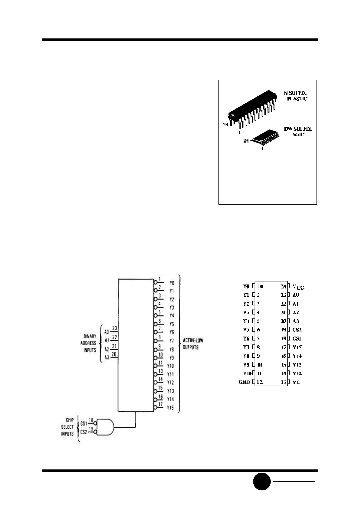
1- of-16 Decoder/Demultiplexer
High-Performance Silicon-Gate CMOS
The SL74HC154 is identical in pinout to the LS/ALS154. The
device inputs are compatible with standard CMOS outputs; with
pullup resistors, they are compatible with LS/ALSTTL outputs.
This device, when enabled, selects one of 16 active-low outputs.
Two active-low Chip Selects are provided to facilitate the chip -select,
demultiplexing, and cascading functions. When either Chip Select is
high, all outputs are high. The demultiplexing function is
accomplished by using the Address inputs to select the desired
device output.
The SL74HC154 is primarily used for memory address decoding
and data routing applications.
• Outputs Directly Interface to CMOS, NMOS, and TTL
• Operating Voltage Range: 2.0 to 6.0 V
• Low Input Current: 1.0 µA
• High Noise Immunity Characteristic of CMOS Devices
LOGIC DIAGRAM
ORDERING INFORMATION
SL74HC154N Plastic
SL74HC154D SOIC
TA = -55° to 125° C for all
packages
PIN ASSIGNMENT
PIN 24 =VCC
PIN 12 = GND
SLS
System Logic
SL74HC154
Semiconductor
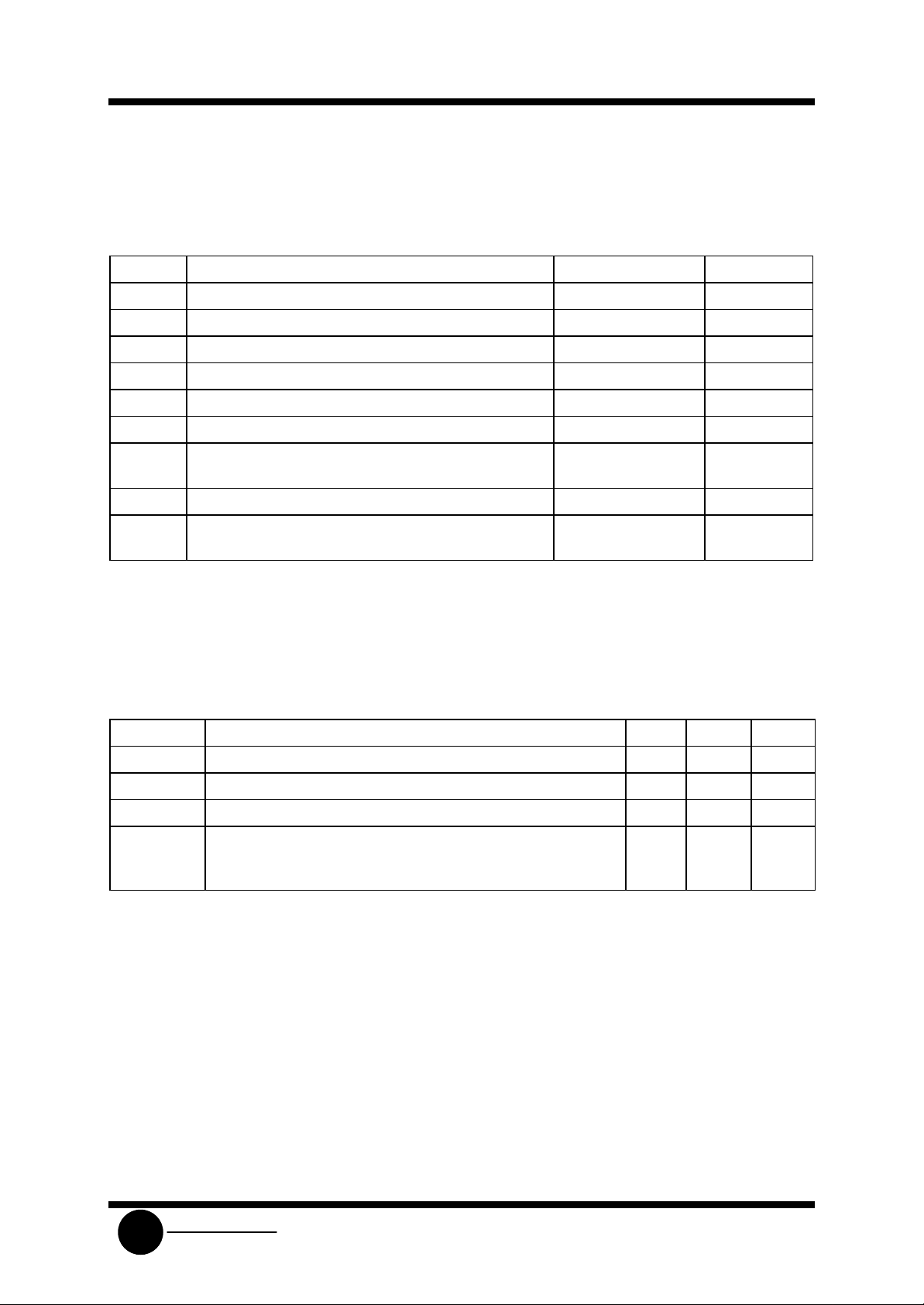
MAXIMUM RATINGS*
Symbol Parameter Value Unit
VCC DC Supply Voltage (Referenced to GND) -0.5 to +7.0 V
VIN DC Input Voltage (Referenced to GND) -1.5 to VCC +1.5 V
V
DC Output Voltage (Referenced to GND) -0.5 to VCC +0.5 V
OUT
IIN DC Input Current, per Pin ±20 mA
I
DC Output Current, per Pin ±25 mA
OUT
ICC DC Supply Current, VCC and GND Pins ±50 mA
PD Power Dissipation in Still Air, Plastic DIP+
SOIC Package+
750
500
Tstg Storage Temperature -65 to +150 °C
TL Lead Temperature, 1 mm from Case for 10 Seconds
260 °C
(Plastic DIP or SOIC Package)
*
Maximum Ratings are those values beyond which damage to the device may occur.
Functional operation should be restricted to the Recommended Operating Conditions.
+Derating - Plastic DIP: - 10 mW/°C from 65° to 125°C
SOIC Package: : - 7 mW/°C from 65° to 125°C
RECOMMENDED OPERATING CONDITIONS
Symbol Parameter Min Max Unit
VCC DC Supply Voltage (Referenced to GND) 2.0 6.0 V
VIN, V
DC Input Voltage, Output Voltage (Referenced to GND) 0 VCC V
OUT
TA Operating Temperature, All Package Types -55 +125 °C
tr, tf Input Rise and Fall Time (Figure 1) VCC =2.0 V
VCC =4.5 V
V
=6.0 V
CC
0
0
0
1000
500
400
mW
ns
This device contains protection circuitry to guard against damage due to high static voltages or electric
fields. However, precautions must be taken to avoid applications of any voltage higher than maximum rated
voltages to this high-impedance circuit. For proper operation, VIN and V
GND≤(VIN or V
OUT
)≤VCC.
should be constrained to the range
OUT
Unused inputs must always be tied to an appropriate logic voltage level (e.g., either GND or VCC).
Unused outputs must be left open.
System Logic
SLS
SL74HC154
Semiconductor
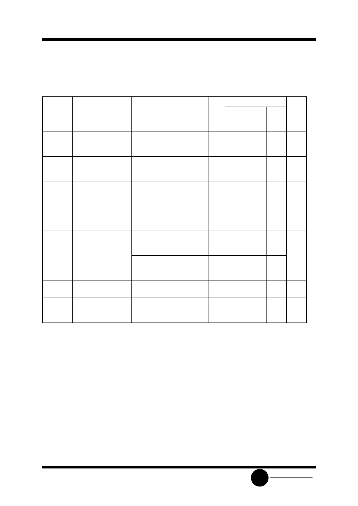
DC ELECTRICAL CHARACTERISTICS(Voltages Referenced to GND)
VCC Guaranteed Limit
Symbol Parameter Test Conditions V 25 °C
to
-55°C
VIH Minimum High-Level
Input Voltage
VIL Maximum Low -Level
Input Voltage
VOH Minimum High-Level
Output Voltage
VIN=VIH or VIL
VOL Maximum Low -Level
Output Voltage
VIN=VIH or VIL
IIN Maximum Input
V
=0.1 V or VCC-0.1 V
OUT
I
≤ 20 µA
OUT
V
=0.1 V or VCC-0.1 V
OUT
I
≤ 20 µA
OUT
VIN=VIH or VIL
I
≤ 20 µA
OUT
I
≤ 4.0 mA
OUT
I
≤ 5.2 mA
OUT
VIN=VIH or VIL
I
≤ 20 µA
OUT
I
≤ 4.0 mA
OUT
I
≤.5.2 mA
OUT
2.0
4.5
6.0
2.0
4.5
6.0
2.0
4.5
6.0
4.5
6.0
2.0
4.5
6.0
4.5
6.0
1.5
3.15
4.2
0.3
0.9
1.2
1.9
4.4
5.9
3.98
5.48
0.1
0.1
0.1
0.26
0.26
VIN=VCC or GND 6.0 ±0.1 ±1.0 ±1.0 µA
Leakage Current
≤85
°C
1.5
3.15
4.2
0.3
0.9
1.2
1.9
4.4
5.9
3.84
5.34
0.1
0.1
0.1
0.33
0.33
≤125
°C
1.5
3.15
4.2
0.3
0.9
1.2
1.9
4.4
5.9
3.7
5.2
0.1
0.1
0.1
0.4
0.4
Unit
V
V
V
V
ICC Maximum Quiescent
Supply Current
(per Package)
VIN=VCC or GND
I
=0µA
OUT
6.0 8.0 80 160 µA
System Logic
SLS
 Loading...