

SLS SL494D, SL494N Datasheet
Semiconductor
PWM Control Circuit
The SL494 incorporates on a single monolithic chip all the
functions required in the construction of a pulse-width-modulation
control circuit. Designed primarily for power supply control, the SL494
contains an on-chip 5-volt regulator, two error amplifiers, adjustable
oscillator, dead-time control comparator, pulse-steering flip -flop, and
output-control circuitry. The uncommitted output transistors provide
either common-emitter or emitter-follower output capability. Push-pull
or single-ended output operation may be selected through the outputcontrol function. The architecture of the IL494 prohibits the possibility
of either output being pulsed twice during push-pull operation.
• Complete PWM Power Control Circuitry
• Uncommitted Outputs for 200 mA Sink or Source
• Output Control Selects Single-Ended or Push-Pull Operation
• Internal Circuitry Prohibits Double Pulse at Either Output
• Internal Regulator Provides a Stable 5 V Reference Supply
• Variable Dead-Time Provides Control Over Total Range
SL494
ORDERING INFORMATION
SL494N Plastic
SL494D SOIC
TA = -20°C to 85° C
for all packages
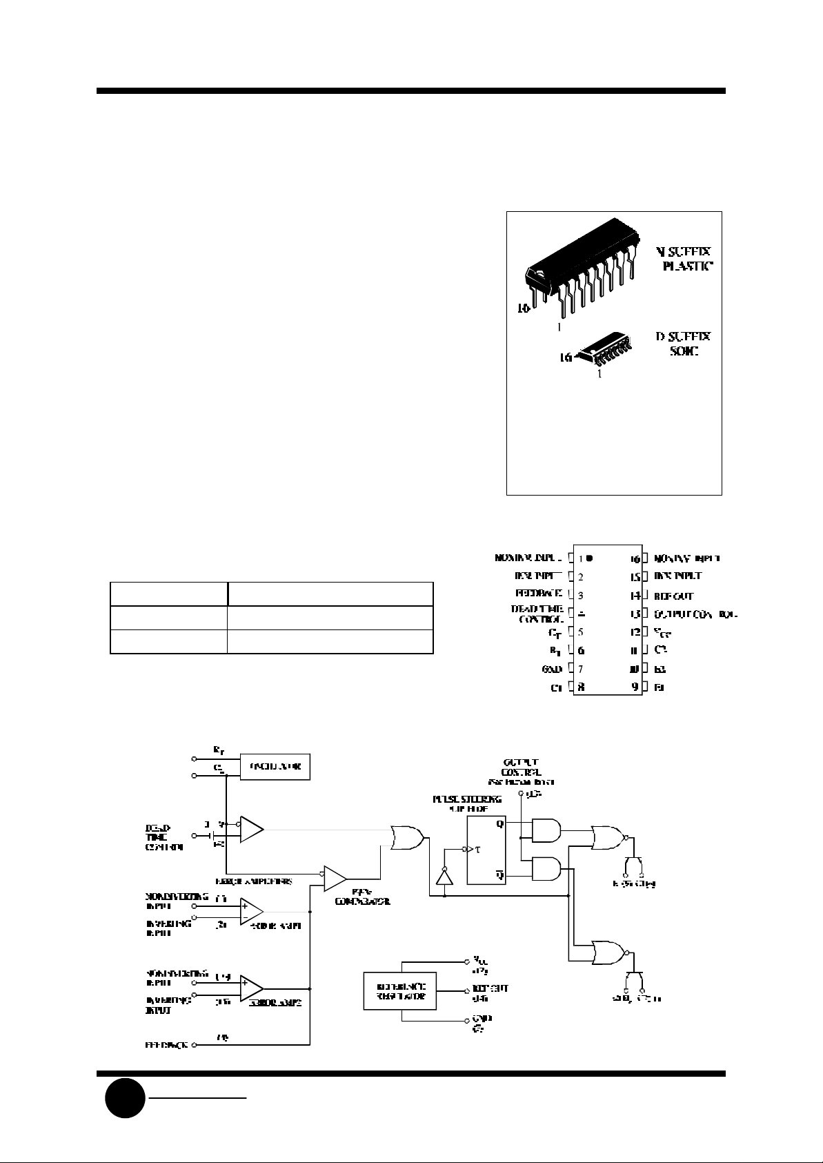
PIN ASSIGNMENT
FUNCTION TABLE
Output Control Output Function
Grounded Single-ended or Parallel Output
At V
Normal Push-Pull Oper ation
ref
LOGIC DIAGRAM
SLS
System Logic
SL494
Semiconductor
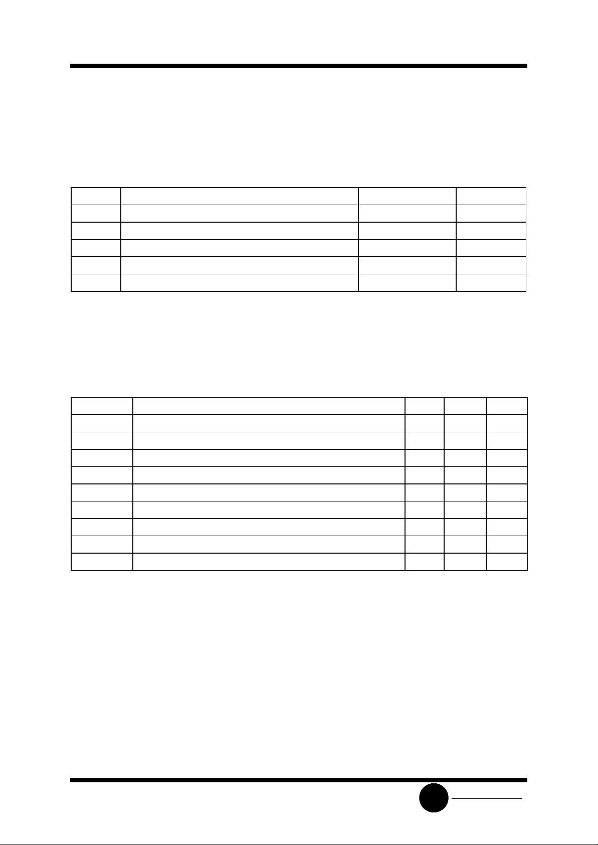
MAXIMUM RATINGS
Symbol Parameter Value Unit
VCC Supply Voltage 41 V
VI Amplifier Input Voltage VCC +0.3 V
VO Collector Output Voltage 41 V
Collector Output Current 250 mA
Tstg Storage Temperature -65 to +150 °C
RECOMMENDED OPERATING CONDITIONS
Symbol Parameter Min Max Unit
VCC Supply Voltage 7 40 V
VI Amplifier Input Voltage -0.3 V
VO Collector Output Voltage 40 V
Collector Output Current (Each Transistor) 200 mA
Current Into Feed back Terminal 0.3 mA
CT Timing Capacitor 0.47 10.000 nF
RT Timing Resistor 1.8 500 KΩ
Oscillator Frequency 1 300 KHz
TA Operating Free-Air Temperature -20 +85 °C
- 2 V
CC
SLS
System Logic
 Loading...