

SLS SL4558D, SL4558N Datasheet
Dual Operational Amplifiers
SL4558
The SL4558 is dual general purpose operational amplifiers.
The high common-mode input voltage range and the absence of
latch-up make these amplifiers ideal for voltage follower application.
The devices are short circuit protected and the internal frequency
compensation ensures stability without external components.
• Short-Circuit Protection
• Wide common-mode and differential ranges
• No frequency compensation required
• Low power consumption
• No latch-up
• 3 MHz unity gain bandwidth guaranteed
• Gain and phase math between amplifiers
ORDERING INFORMATION
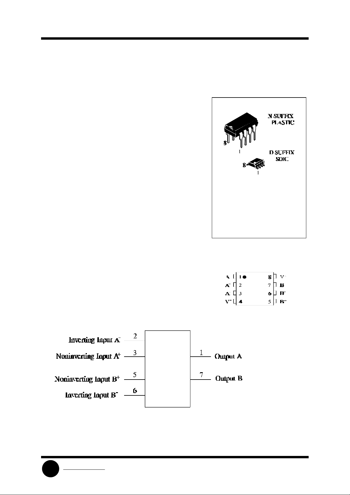
SL4558N Plastic
SL4558D SOIC
TA = 0° to 70° C for
all packages
PIN ASSIGNMENT
System Logic
SLS
Semiconductor
LOGIC DIAGRAM
Pin 4 = Supply Voltage V-
Pin 8 = Supply Voltage V+
SL4558
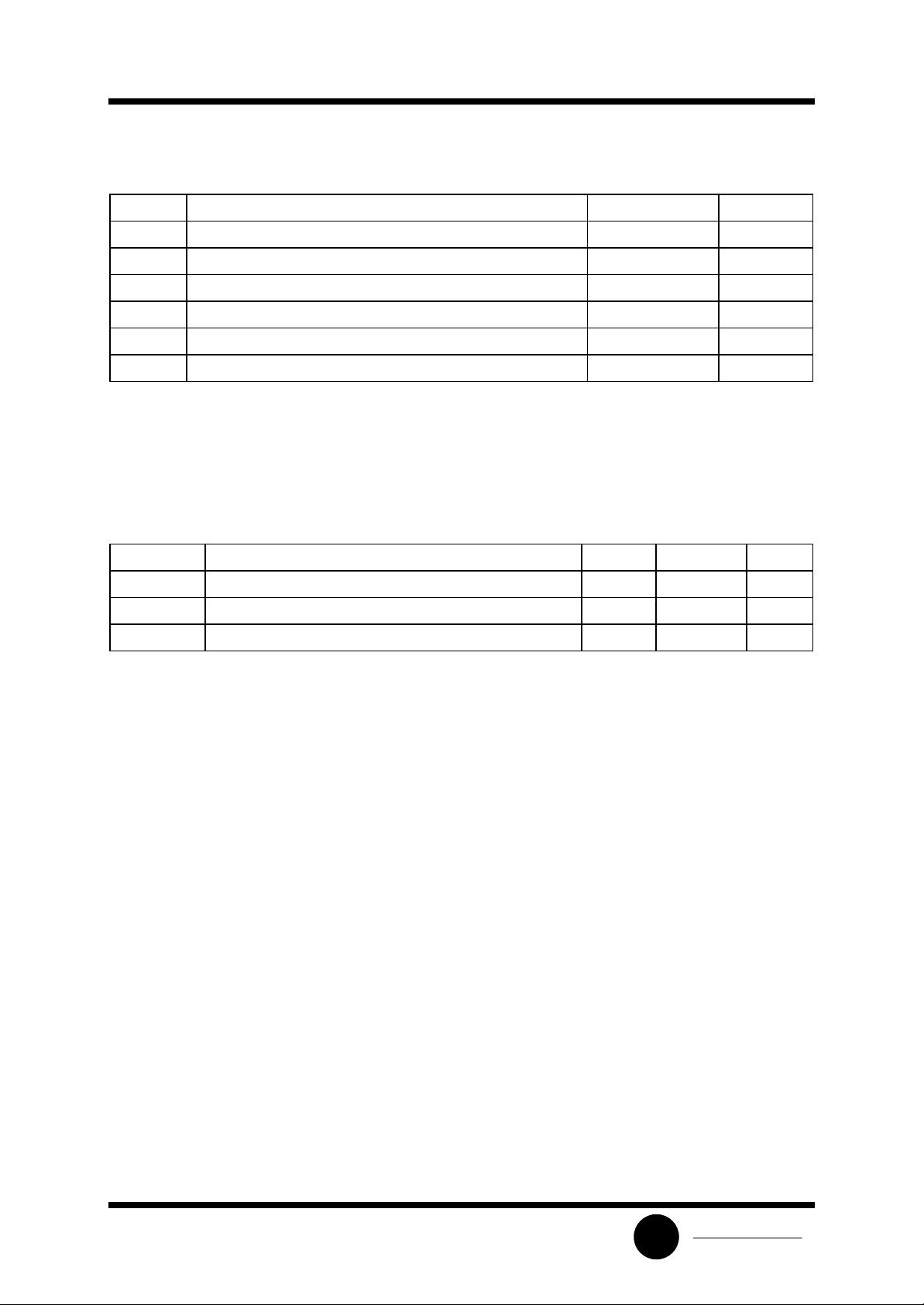
MAXIMUM RATINGS*
Symbol Parameter Value Unit
V+ Supply Voltage +18 V
V- Supply Voltage -18 V
V
Differential Input Voltage ±30 V
IDR
VIN Input Voltage ±15 V
PD Power Dissipation in Still Air 570 mW
Tstg Storage Temperature Range -55 to +125 °C
*
Maximum Ratings are those values beyond which damage to the device may occur.
Functional operation should be restricted to the Recommended Operating Conditions.
RECOMMENDED OPERATING CONDITIONS
Symbol Parameter Min Max Unit
V+ Supply Voltage +15 V
V- Supply Voltage -15 V
TA Operating Temperature, All Pakage Types 0 +70 °C
This device contains protection circuitry to guard against damage due to high static voltages or electric
fields. However, precautions must be taken to avoid applications of any voltage higher than maximum rated
voltages to this high-impedance circuit. For proper operation, VIN and V
GND≤(VIN or V
Unused inputs must always be tied to an appropriate logic voltage level (e.g., either GND or VCC).
Unused outputs must be left open.
OUT
)≤VCC.
should be constrained to the range
OUT
System Logic
SLS
Semiconductor
 Loading...