

SLS SL4541BD, SL4541BN Datasheet
SL4541B
Semiconductor
Programmable Timer
High-Performance Silicon-Gate CMOS
The SL4541 programmable timer consists of a 16-stage binary
counter, an oscillator that is controlled by external R-C components (2
resistors and a capacitor), an automatic power-on reset circuit, and
output control logic. The counter increments on positive-edge clock
transitons and can also be reset via the MASTER RESET input.
The output from this timer is the Q or not Q output from the 8th,
10th, 13th, or 16th counter stage. The desired stage is chosen using
time-select inputs A and B. The output is available in either of two
modes selectable via the MODE input, pin 10. When this MODE input
is a logic “1”,the output will be a continuous square wave having a
frequency equal to the oscillator frequency divided by 2N. With the
MODE input set to logic ”0” and after a MASTER RESET is initiated,
the output (assuming Q output has been selected) changes from a low
to a high state after 2
MASTER RESET pulse is applied or the MODE input is set to a logic
“1”.
Timing is initialized by setting the AUTO RESET input (pin 5) to logic “0”and turning power on. If pin 5 is set
to logic “1”, the AUTO RESET circuit is disabled and counting will not start untill after a positive MASTER
RESET pulse is applied and returns to a low level. The AUTO RESET consumes an appreciable amount of power
and should not be used if low-power operation is desired. For reliable automatic power-on reset, VCC should be
greater than 5V.
• Operating Voltage Range: 3.0 to 18 V
• Maximum input current of 1 µA at 18 V over full package-temperature range; 100 nA at 18 V and 25°C
• Noise margin (over full package temperature range):
N-1
counts and remains in that state until another
1.0 V min @ 5.0 V supply
2.0 V min @ 10.0 V supply
2.5 V min @ 15.0 V supply
ORDERING INFORMATION
SL4541BN Plastic
SL4541BD SOIC
TA = -55° to 125° C for all packages
SLS
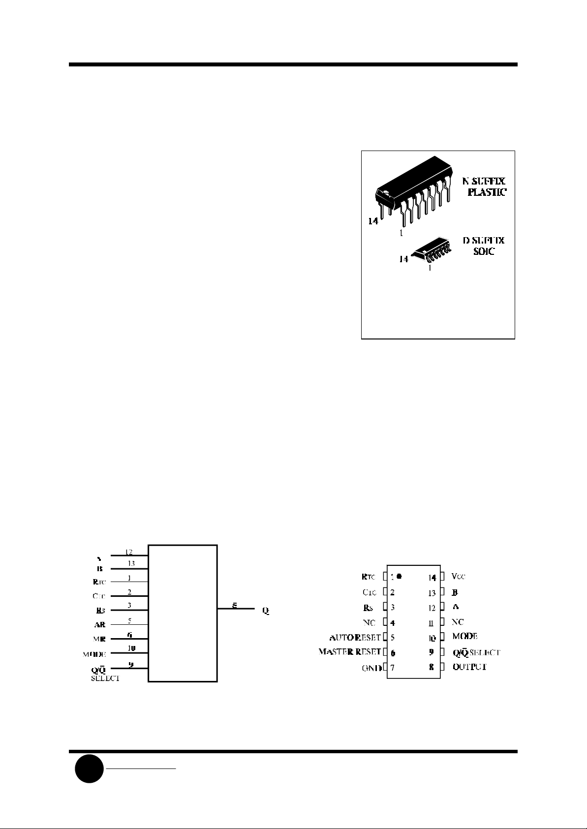
LOGIC DIAGRAM
PIN 14 =V
PIN 7 = GND
PINS 4,11 = NO CONNECTION
System Logic
CC
PIN ASSIGNMENT
NC = NO CONNECTION
SL4541B
Semiconductor
MAXIMUM RATINGS*
Symbol Parameter Value Unit
VCC DC Supply Voltage (Referenced to GND) -0.5 to +20 V
VIN DC Input Voltage (Referenced to GND) -0.5 to VCC +0.5 V
V
DC Output Voltage (Referenced to GND) -0.5 to VCC +0.5 V
OUT
IIN DC Input Current, per Pin ±10 mA
PD Power Dissipati on in Still Air, Plastic DIP+
SOIC Package+
PD Power Dissipation per Output Transistor 100 mW
Tstg Storage Temperature -65 to +150 °C
TL Lead Temperature, 1 mm from Case for 10 Seconds
(Plastic DIP or SOIC Package)
*
Maximum Ratings are those values beyond which damage to the device may occur.
Functional operation should be restricted to the Recommended Operating Conditions.
+Derating - Plastic DIP: - 10 mW/°C from 65° to 125°C
SOIC Package: : - 7 mW/°C from 65° to 125°C
750
500
260 °C
mW
RECOMMENDED OPERATING CONDITIONS
Symbol Parameter Min Max Unit
VCC DC Supply Voltage (Referenced to GND) 3.0 18 V
VIN, V
fields. However, precautions must be taken to avoid applications of any voltage higher than maximum rated
voltages to this high-impedance circuit. For proper operation, VIN and V
GND≤(VIN or V
Unused outputs must be left open.
DC Input Voltage, Output Voltage (Referenced to GND) 0 VCC V
OUT
TA Operating Temperature, All Package Types -55 +125 °C
This device contains protection circuitry to guard against damage due to high static voltages or electric
should be constrained to the range
OUT
)≤VCC.
OUT
Unused inputs must always be tied to an appropriate logic voltage level (e.g., either GND or VCC).
SLS
System Logic
 Loading...