

SLS SL4060BD, SL4060BN Datasheet
Semiconductor
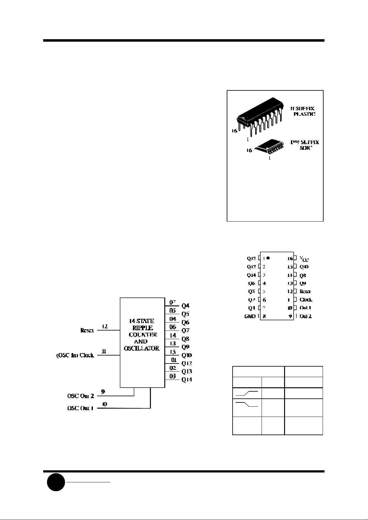
14-Stage Ripple-Carry Binary
Counter/Divider and Oscillator
High-Voltage Silicon-Gate CMOS
The SL4060B consists of an oscillator section and 14 ripple -carry
binary counter stages. The oscillator configuration allows design of
either RC or crystal oscillator circuits. A RESET input is provided
which resets the counter to the all-Q’s state and disables the oscillator.
A high level on the RESET line accomplishes the reset function. All
counter stages are master-slave flip -flops. The state of the counter is
advanced one step in binary order on the negative transition of OSC In
(and OSC Out). Schmitt trigger action on the input-pulse line permits
unlimited input-pulse rise and fall times.
• Operating Voltage Range: 3.0 to 18 V
• Maximum input current of 1 µA at 18 V over full package-
temperature range; 100 nA at 18 V and 25°C
• Noise margin (over full package temperature range):
1.0 V min @ 5.0 V supply
2.0 V min @ 10.0 V supply
2.5 V min @ 15.0 V supply
SL4060B
ORDERING INFORMATION
SL4060BN Plastic
SL4060BD SOIC
TA = -55° to 125° C for all
packages
PIN ASSIGNMENT
LOGIC DIAGRAM
PIN 16=VCC
PIN 8= GND
FUNCTION TABLE
Inputs Outputs
Osc In Reset Q
L No change
L Advance to
X H All Outputs
X = don’t care
next state
are low
SLS
System Logic
SL4060B
Semiconductor
MAXIMUM RATINGS*
Symbol Parameter Value Unit
VCC DC Supply Voltage (Referenced to GND) -0.5 to +20 V
VIN DC Input Voltage (Referenced to GND) -0.5 to VCC +0.5 V
V
DC Output Voltage (Referenced to GND) -0.5 to VCC +0.5 V
OUT
IIN DC Input Current, per Pin ±10 mA
PD Power Dissipation in Still Air, Plastic DIP+
SOIC Package+
PD Power Dissipation per Output Transistor 100 mW
Tstg Storage Temperature -65 to +150 °C
TL Lead Temperature, 1 mm from Case for 10 Seconds
(Plastic DIP or SOIC Package)
*
Maximum Ratings are those values beyond which damage to the device may occur.
Functional operation should be restricted to the Recommended Operating Conditions.
+Derating - Plastic DIP: - 10 mW/°C from 65° to 125°C
SOIC Package: : - 7 mW/°C from 65° to 125°C
750
500
260 °C
RECOMMENDED OPERATING CONDITIONS
Symbol Parameter Min Max Unit
VCC DC Supply Voltage (Referenced to GND) 3.0 18 V
VIN, V
DC Input Voltage, Output Voltage (Referenced to GND) 0 VCC V
OUT
TA Operating Temperature, All Package Types -55 +125 °C
mW
This device contains protection circuitry to guard against damage due to high static voltages or electric
fields. However, precautions must be taken to avoid applications of any voltage higher than maximum rated
voltages to this high-impedance circuit. For proper operation, VIN and V
GND≤(VIN or V
Unused inputs must always be tied to an appropriate logic voltage level (e.g., either GND or VCC).
Unused outputs must be left open.
OUT
)≤VCC.
should be constrained to the range
OUT
System Logic
SLS
 Loading...