

SLS SL4052BD, SL4052BN Datasheet
Semiconductor
Analog Multiplexer Demultiplexer
High-Performance Silicon-Gate CMOS
The SL4052B analog multiplexer/demultiplexer is digitally controlled
analog switches having low ON impedance and very low OFF leakage
current. Control of analog signals up to 20V peak-to-peak can be
achieved by digital signal amplitudes of 4.5 to 20V (if VCC - GND = 3V, a
VCC - VEE of up to 13 V can be controlled; for VCC - VEE level differences
above 13V a VCC - GND of at least 4.5V is required).
These multiplexer circuits dissipate extremely low quiescent power
over the full V
independent of the logic state of the control signals. When a logic
“1”is present at the ENABLE input terminal all channels are off.
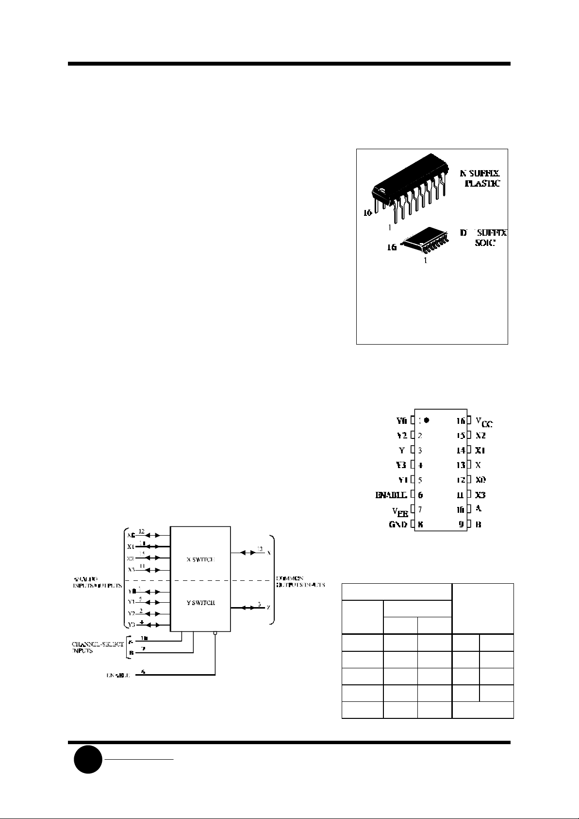
The SL4052 is a differential 4-channel multiplexer having two binary
control inputs. A and B, and an enable input. The two binary input
signals select 1 of 4 pairs of channels to turned on and connect the
analog inputs to the outputs.
• Operating Voltage Range: 3.0 to 18 V
• Maximum input current of 1
µA at 18 V over full package-temperature range; 100 nA at 18 V and
25°C
• Noise margin (over full package temperature range):
-GND and VCC - VEE supply-voltage ranges,
CC
1.0 V min @ 5.0 V supply
2.0 V min @ 10.0 V supply
2.5 V min @ 15.0 V supply
SL4052B
ORDERING INFORMATION
SL4052BN Plastic
SL4052BD SOIC
TA = -55° to 125° C for all packages
PIN ASSIGNMENT
SLS
LOGIC DIAGRAM
Double-Pole, 4-Position
System Logic
Plus Common Off
PIN 16 =V
PIN 7 = VEE
PIN 8 = GND
CC
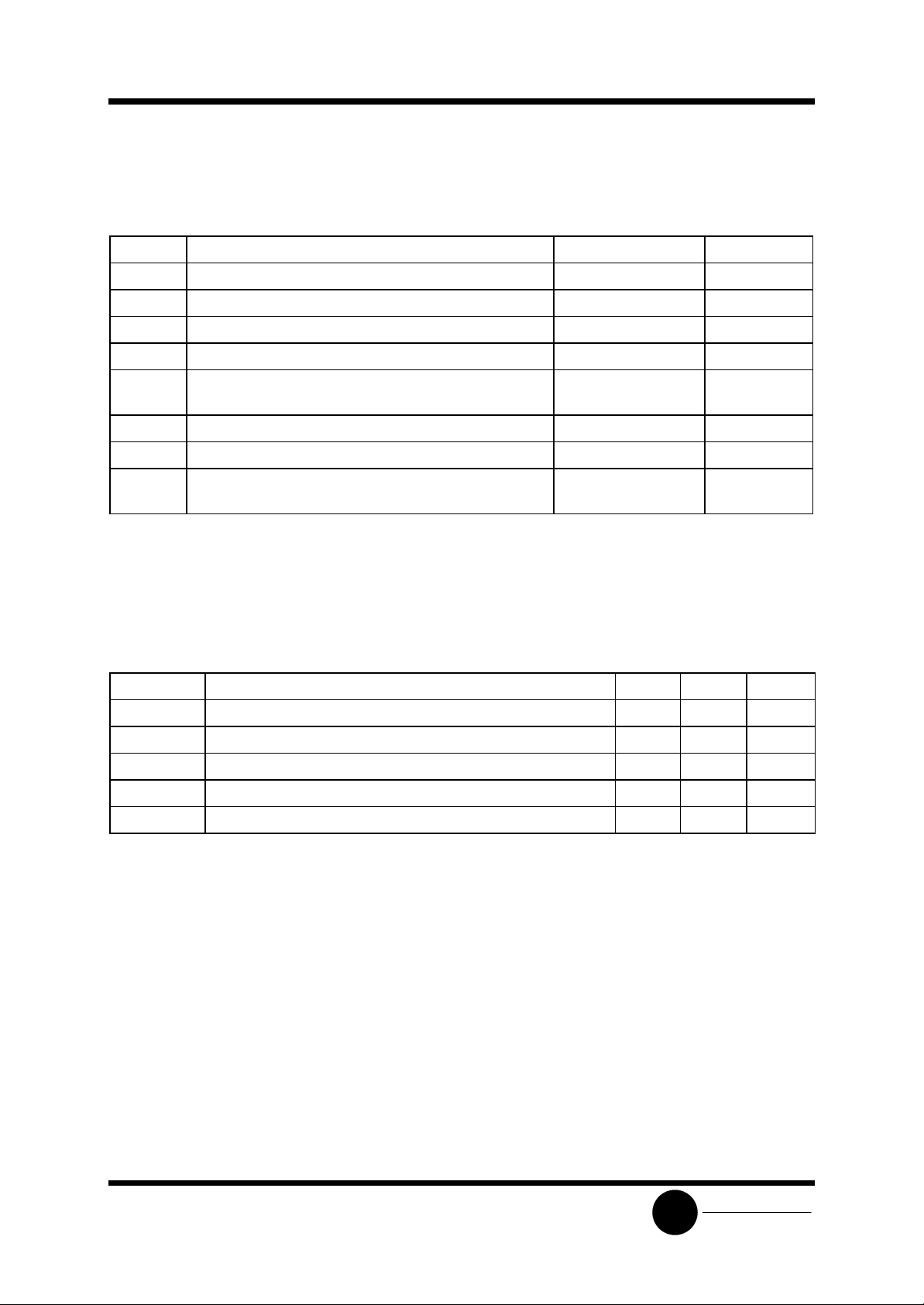
FUNCTION TABLE
Control Inputs ON
Enable Select Channels
B A
L L L Y0 X0
L L H Y1 X1
L H L Y2 X2
L H H Y3 X3
H X X None
X = don’t care
SL4052B
Semiconductor
MAXIMUM RATINGS*
Symbol Parameter Value Unit
VCC DC Supply Voltage (Referenced to GND) -0.5 to +20 V
VIN DC Input Voltage (Referenced to GND) -0.5 to VCC +0.5 V
V
DC Output V oltage (Referenced to GND) -0.5 to VCC +0.5 V
OUT
IIN DC Input Current, per Pin ±10 mA
PD Power Dissipation in Still Air, Plastic DIP+
SOIC Package+
750
500
mW
PD Power Dissipation per Output Transistor 100 mW
Tstg Storage Temperature -65 to +150 °C
TL Lead Temperature, 1 mm from Case for 10 Seconds
260 °C
(Plastic DIP or SOIC Package)
*
Maximum Ratings are those values beyond which damage to the device may occur.
Functional operation should be restricted to the Recommended Operating Conditions.
+Derating - Plastic DIP: - 10 mW/°C from 65° to 125°C
SOIC Package: : - 7 mW/°C from 65° to 125°C
RECOMMENDED OPERATING CONDITIONS
Symbol Parameter Min Max Unit
VCC DC Supply Voltage (Referenced to GND) 3.0 18 V
VIN, V
*
In certain applications, the external load-resistor current may include both VCC and signal -line components.
fields. However, precautions must be taken to avoid applications of any voltage higher than maximum rated
voltages to this high-impedance circuit. For proper operation, VIN and V
GND≤(VIN or V
Analog I/O pins may be left open or terminated.
DC Input Voltage, Output Voltage (Referenced to GND) 0 VCC V
OUT
TA Operating Temperature, All Package Types -55 +125 °C
I Multiplexer Switch Input Current Capability* - 25 mA
ROH Output Load Resistance 100 - Ω
This device contains protection circuitry to guard against damage due to high static voltages or electric
should be constrained to the range
OUT
)≤VCC.
OUT
Unused digital pins must be tied to an appropriate logic voltage level (e.g., either GND or VCC). Unused
SLS
System Logic
 Loading...