

SLS SL4029BDW, SL4029BN Datasheet
SL4029B
Semiconductor
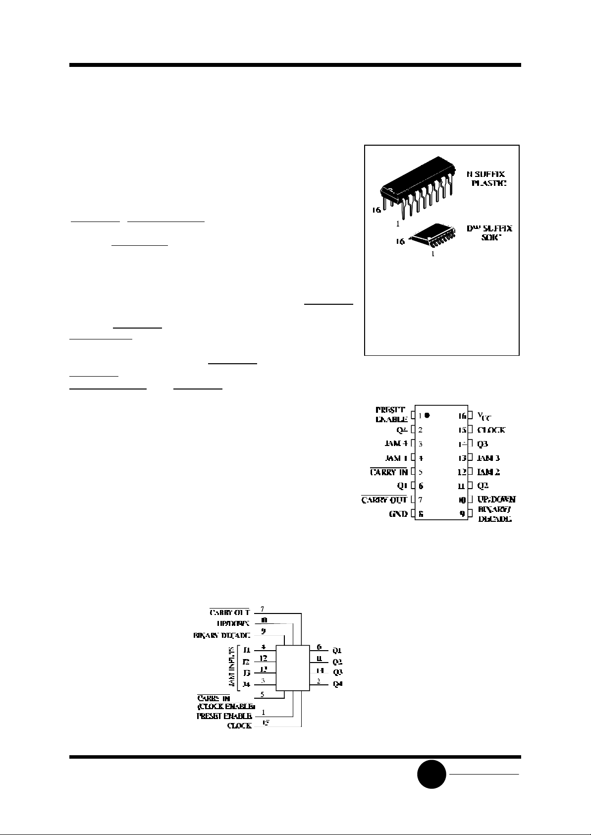
Presettable Up/Down Counter
High-Voltage Silicon-Gate CMOS
The SL4029B consists of a four-stage binary or BCD-decade
up/down counter with provisions for look -ahead carry in both counting
modes. The inputs consists of a single CLOCK,
CARRY IN,(CLOCK ENABLE), BINARY/DECADE, UP/DOWN,
PRESET ENABLE, and four individual JAM signals. Q1, Q2, Q3, Q4 and
a CARRY OUT signal are provided as outputs.
A high PRESET ENABLE signal allows information on the JAM
INPUTS to preset the counter to any state asynchronously with the
clock. A low on each JAM line, when the PRESET -ENABLE signal is
high, resets the counter to its zero count. The counter is advanced one
count at the positive transition of the clock when the CARRY IN and
PRESET ENABLE signals are low. Advancement is inhibited when the
CARRY IN or PRESET ENABLE signals are high. The CARRY OUT
signal is normally high and goes low when the counter reaches its
maximum count in the UP mode or the minimum count in the DOWN
mode provided the CARRY IN signal is low. The CARRY IN signal
in the low state can thus be considered a CLOCK ENABLE. The
CARRY IN terminal must be connected to GND when not in use.
Binary counting is accomplished when the BINARY/DECADE
input is high; the counter counts in the decade mode when the
BINARY/DECADE input is low. The counter counts up when the
UP/DOWN input is high, and down when the UP/DOWN input is
low.
Parallel clocking pr ovides synchronous control and hence faster
response from all counting outputs. Ripple-clocking allows for
longer clock input rise and fall times.
• Operating Voltage Range: 3.0 to 18 V
• Maximum input current of 1 µA at 18 V over full package-
temperature range; 100 nA at 18 V and 25°C
• Noise margin (over full package temperature range):
1.0 V min @ 5.0 V supply
2.0 V min @ 10.0 V supply
2.5 V min @ 15.0 V supply
ORDERING INFORMATION
SL4029BN Plastic
SL4029BDW SOIC
TA = -55° to 125° C for all packages
PIN ASSIGNMENT
LOGIC DIAGRAM
PIN 16=V
PIN 8= GND
CC
SLS
System Logic
SL4029B
Semiconductor
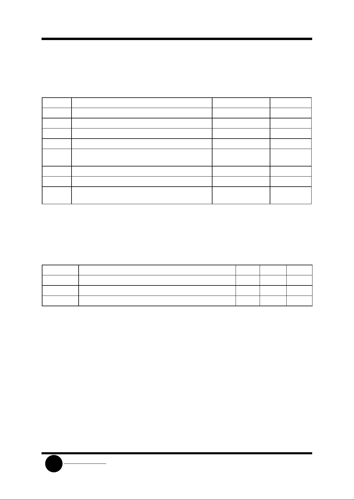
MAXIMUM RATINGS*
Symbol Parameter Value Unit
VCC DC Supply Voltage (Referenced to GND) -0.5 to +20 V
VIN DC Input Voltage (Referenced to GND) -0.5 to VCC +0.5 V
V
DC Output Voltage (Referenced to GND) -0.5 to VCC +0.5 V
OUT
IIN DC Input Current, per Pin ±10 mA
PD Power Dissipation in Still Air, Plastic DIP+
SOIC Package+
PD Power Dissipation per Output Transistor 100 mW
Tstg Storage Temperature -65 to +150 °C
TL Lead Temperature, 1 mm from Case for 10 Seconds
(Plastic DIP or SOIC Package)
*
Maximum Ratings are those values beyond which damage to the device may occur.
Functional operation should be restricted to the Recommended Operating Conditions.
+Derating - Plastic DIP: - 10 mW/°C from 65° to 125°C
SOIC Package: : - 7 mW/°C from 65° to 125°C
750
500
260 °C
RECOMMENDED OPERATING CONDITIONS
Symbol Parameter Min Max Unit
VCC DC Supply Voltage (Referenced to GND) 3.0 18 V
VIN, V
DC Input Voltage, Output Voltage (Referenced to GND) 0 VCC V
OUT
TA Operating Temperature, All Package Types -55 +125 °C
mW
This device contains protection circuitry to guard against damage due to high static voltages or electric
fields. However, precautions must be taken to avoid applications of any voltage higher than maximum rated
voltages to this high-impedance circuit. For proper operation, VIN and V
GND≤(VIN or V
Unused inputs must always be tied to an appropriate logic voltage level (e.g., either GND or VCC).
Unused outputs must be left open.
System Logic
SLS
OUT
)≤VCC.
should be constrained to the range
OUT
SL4029B
Semiconductor
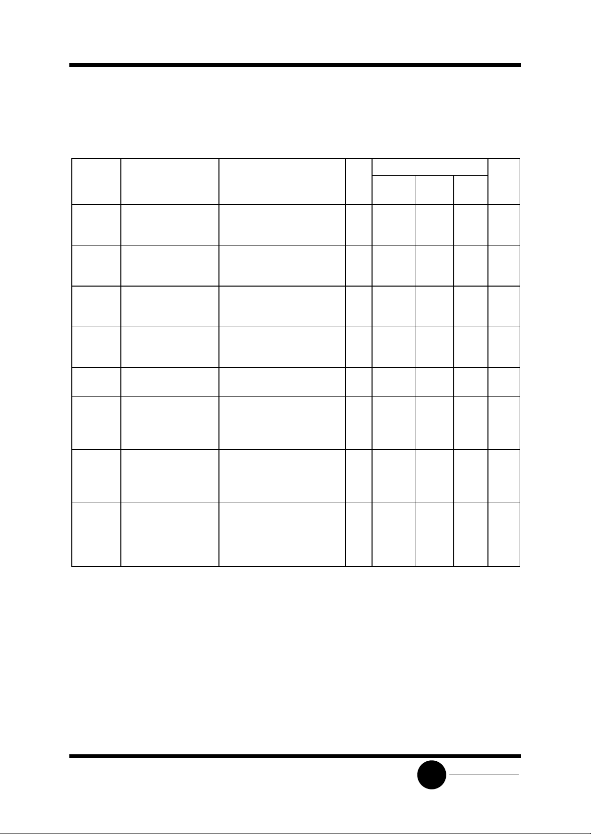
DC ELECTRICAL CHARACTERISTICS(Voltages Referenced to GND)
VCC Guaranteed Limit
Symbol Parameter Test Conditions V ≥-55°C 25°C ≤125
°C
VIH Minimum High-Level
Input Voltage
VIL Maximum Low -Level
Input Voltage
VOH Minimum High-Level
Output Voltage
VOL Maximum Low -Level
Output Voltage
IIN Maximum Input
V
= 0.5 V or V
OUT
V
= 1.0 V or V
OUT
V
= 1.5 V or V
OUT
V
= 0.5 V or V
OUT
V
= 1.0 V or V
OUT
V
= 1.5 V or V
OUT
VIN=GND or VCC 5.0
VIN=GND or VCC 5.0
- 0.5V
CC
- 1.0 V
CC
- 1.5V
CC
- 0.5V
CC
- 1.0 V
CC
- 1.5V
CC
5.0
10
15
5.0
10
15
10
15
10
15
3.5
7
11
1.5
3
4
4.95
9.95
14.95
0.05
0.05
0.05
3.5
7
11
1.5
3
4
4.95
9.95
14.95
0.05
0.05
0.05
3.5
7
11
1.5
3
4
4.95
9.95
14.95
0.05
0.05
0.05
VIN= GND or VCC 18 ±0.1 ±0.1 ±1.0 µA
Leakage Current
ICC Maximum Quiescent
Supply Current
(per Package)
IOL Minimum Output Low
(Sink) Current
VIN= GND or VCC 5.0
10
15
20
VIN= GND or VCC
UOL=0.4 V
UOL=0.5 V
UOL=1.5 V
5.0
10
15
5
10
20
100
0.64
1.6
4.2
5
10
20
100
0.51
1.3
3.4
150
300
600
3000
0.36
0.9
2.4
Unit
V
V
V
V
µA
mA
IOH Minimum Output High
(Source) Current
VIN= GND or VCC
UOH=2.5 V
UOH=4.6 V
UOH=9.5 V
UOH=13.5 V
5.0
5.0
10
15
-2
-0.64
-1.6
-4.2
-1.6
-0.51
-1.3
-3.4
SLS
-1.15
-0.36
-0.9
-2.4
System Logic
mA
 Loading...