

SLS SL4017BD, SL4017BN Datasheet
Semiconductor
Counter/Divider
High-Voltage Silicon-Gate CMOS
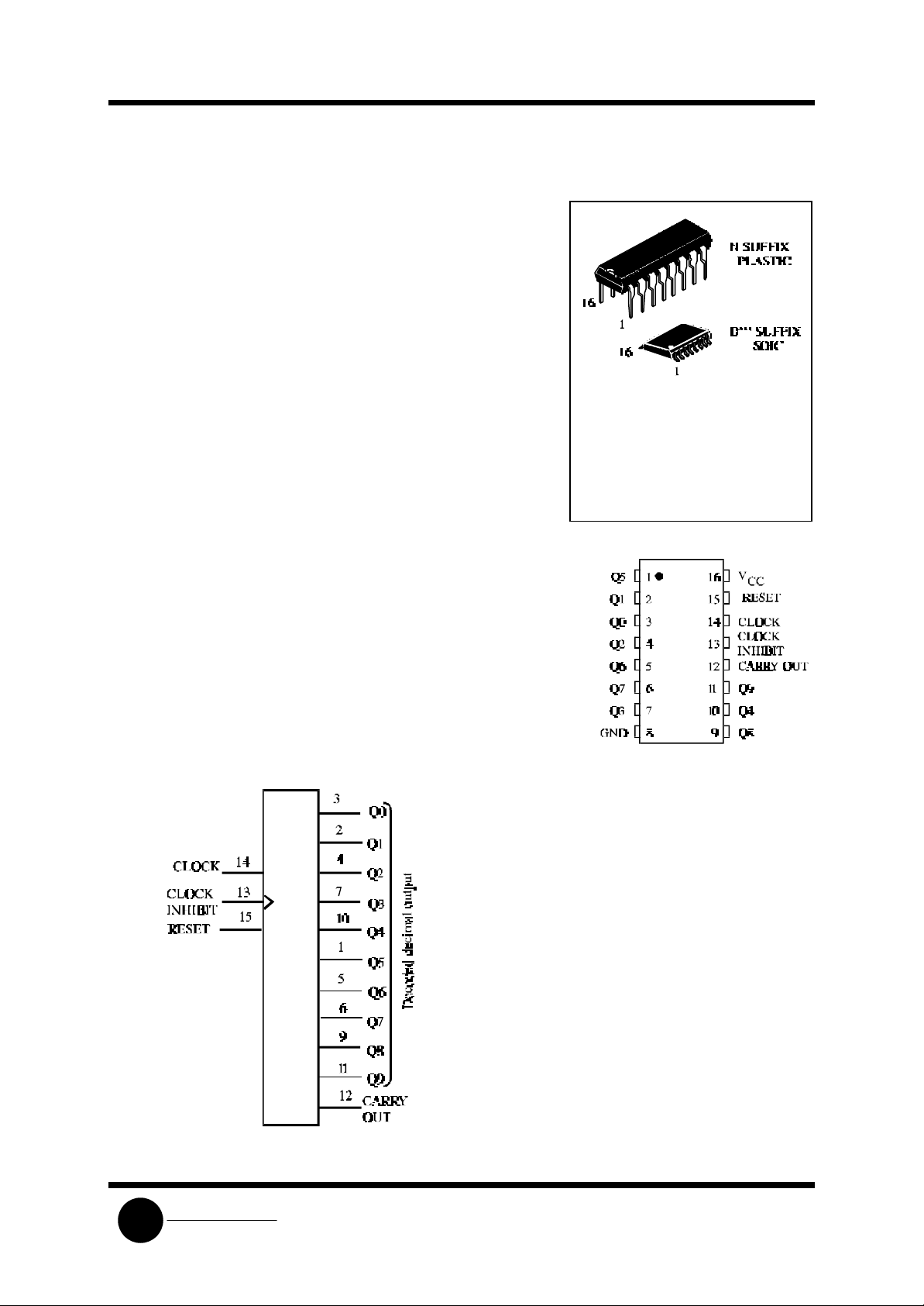
The SL4017B is 5-stage Johnson counter having 10
decoded outputs. Inputs include a CLOCK, a RESET, and a
CLOCK INHIBIT signal. Schmitt trigger action in the
CLOCK input circuit provides pulse shaping that allows
unlimited clock input pulse rise and fall times.
The counter is advanced one count at the positive
clock signal transition if the CLOCK INHIBIT signal is
low. Counter advancement via the clock line is inhibited
when the CLOCK INHIBIT signal is high. A high RESET
signal clears the counter to its zero count. Use of the
Johnson counter configuration permits high-speed
operation, 2-input decode-gating and spike-free decoded
outputs. Anti-lock gating is provided, thus assuring proper
counting sequence. The decoded outputs are normally low
and go high only at their respective decoded time slot.
Each decoded output remains high for one full clock cycle.
A CARRY-OUT signal completes one cycle every 10 clock
input cycles in the SL4017B.
• Operating Voltage Range: 3.0 to 18 V
• Maximum input current of 1 µA at 18 V over full
package-temperature range; 100 nA at 18 V and 25°C
SL4017B
ORDERING INFORMATION
SL4017BN Plastic
SL4017BD SOIC
TA = -55° to 125° C for all
packages
PIN ASSIGNMENT
SL
LOGIC DIAGRAM
PIN 16 =V
PIN 8 = GND
System Logic
• Noise margin (over full package
temperature range):
1.0 V min @ 5.0 V supply
2.0 V min @ 10.0 V supply
2.5 V min @ 15.0 V supply
CC
SL4017B
Semiconductor
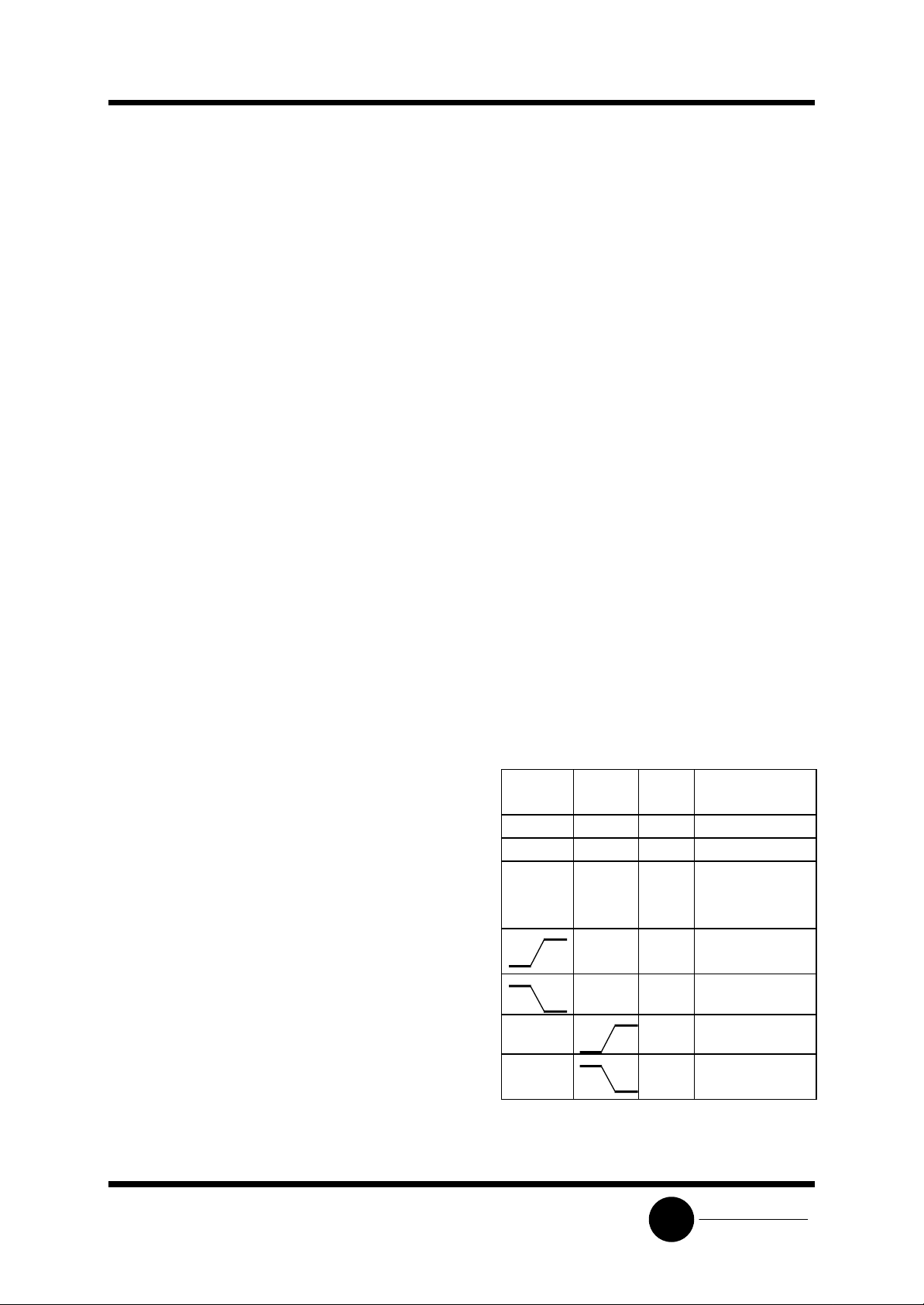
FUNCTION TABLE
Clock Clock
Enable
L X L no change
X H L no change
X X H reset counter
X L no change
H L Advance to
* Carry Out=H for Q0,Q1,Q2,Q3 or Q4=H
Carry Out = L otherwise, X=don’t care
Reset Output State *
Q0=H, Q1Q9=L, C0=H
L L Advance to
next state
X L no change
next state
SL
System Logic
SL4017B
Semiconductor
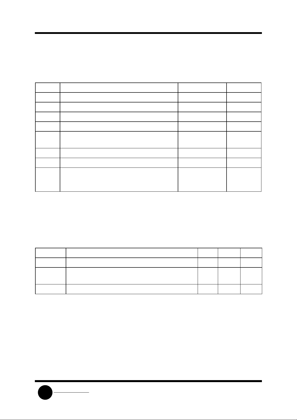
MAXIMUM RATINGS
*
Symbol Parameter Value Unit
V
CC
V
V
OUT
I
IN
P
P
DC Supply Voltage (Referenced to GND) -0.5 to +20 V
DC Input Voltage (Referenced to GND) -0.5 to VCC +0.5 V
IN
DC Output Voltage (Referenced to GND) -0.5 to VCC +0.5 V
DC Input Current, per Pin ±10 mA
Power Dissipation in Still Air, Plastic DIP+
D
SOIC Package+
Power Dissipation per Output Transistor 100 mW
D
750
500
mW
Tstg Storage Temperature -65 to +150 °C
T
Lead Temperature, 1 mm from Case for 10
L
260 °C
Seconds
(Plastic DIP or SOIC Package)
*
Maximum Ratings are those values beyond which damage to the device may occur.
Functional operation should be restricted to the Recommended Operating Conditions.
+Derating - Plastic DIP: - 10 mW/°C from 65° to 125°C
SOIC Package: : - 7 mW/°C from 65° to 125°C
RECOMMENDED OPERATING CONDITIONS
Symbol Parameter Min Max Unit
V
CC
VIN, V
OUT
T
A
This device contains protection circuitry to guard against damage due to high static
voltages or electric fields. However, precautions must be taken to avoid applications of any
voltage higher than maximum rated voltages to this high-impedance circuit. For proper
operation, VIN and V
Unused inputs must always be tied to an appropriate logic voltage level (e.g., either
GND or VCC). Unused outputs must be left open.
DC Supply Voltage (Referenced to GND) 3.0 18 V
DC Input Voltage, Output Voltage (Referenced to
0 V
CC
V
GND)
Operating Temperature, All Package Types -55 +125 °C
should be constrained to the range GND ≤(VIN or V
OUT
OUT
)≤VCC.
SL
System Logic
 Loading...