

SLS SL339D, SL339N Datasheet
Quad Single Supply Comparator
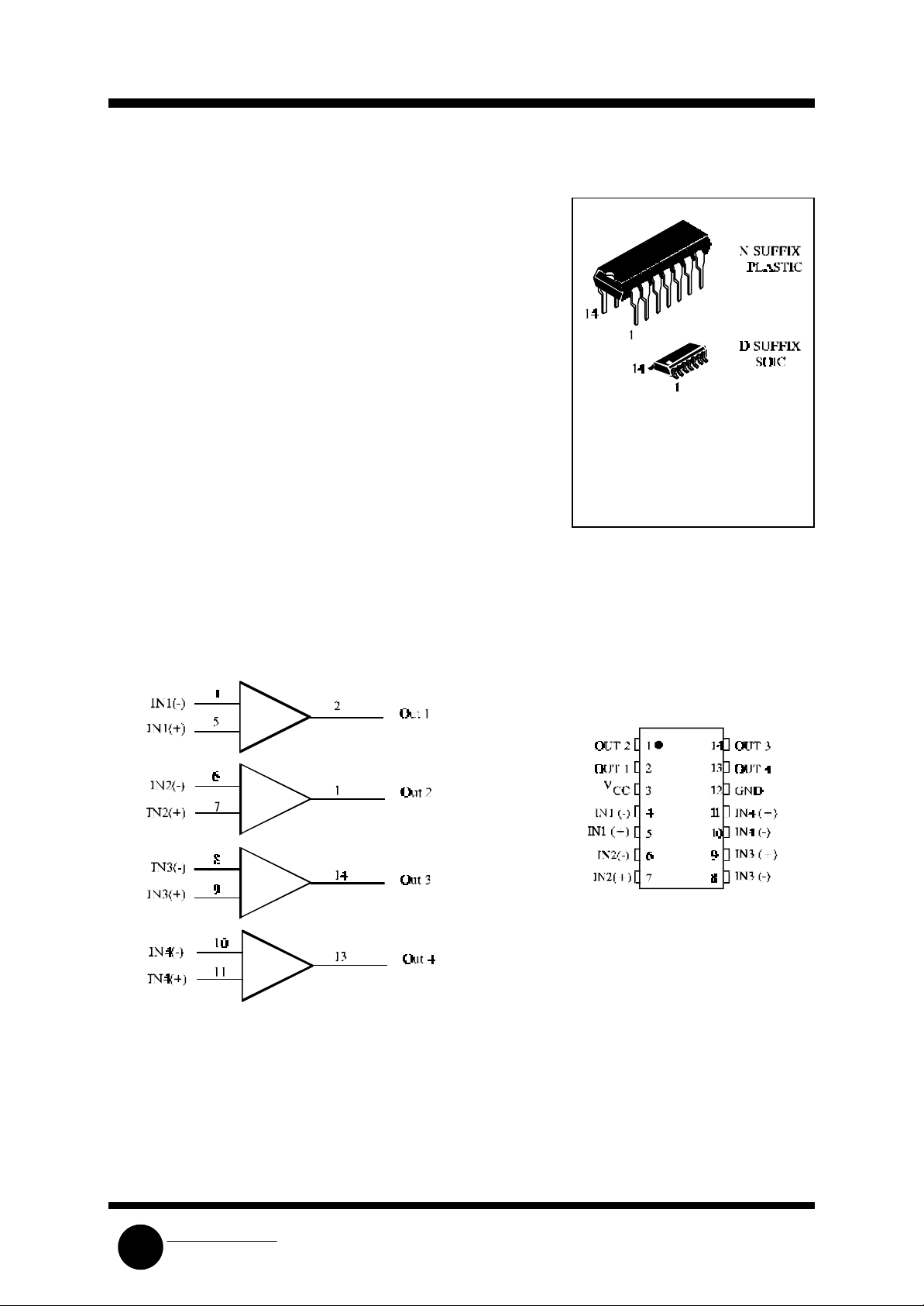
The SL339 consists of four independent precision voltage
comparators with an offset voltage specification as low as 2.0 mV max
for four comparators which were designed specifically to operate from a
single power supply over a wide range of voltages.
Application areas include limit comparators, simple analog to digital
converters; pulse, squarewave and time delay generators; wide range
VCO; MOS clock timers; multivibrators and high voltage digital logic
gates.
• Single or Split Supply Operation
• Low Input Bias Current
• Low Input Offset Current
• Input Common Mode Voltage Range to Gnd
• Low Output Saturation Voltage
• TTL and CMOS Compatible
SL339
ORDERING INFORMATION
SL339N Plastic
SL339D SOIC
TA = 0° to 70° C for all packages.
LOGIC DIAGRAM
PIN 3 = VCC
PIN 12 = GND
PIN ASSIGNMENT
System Logic
SLS
Semiconductor
SL339
MAXIMUM RATINGS*
Symbol Parameter Value Unit
VCC Power Supply Voltages
Single Supply
Split Supplies
V
Input Differential Voltage Range 36 V
IDR
V
Input Common Mode Voltage Range (1) -0.3 to VCC V
ICR
36
±18
ISC Output Short Circuit to Ground Continuous
IIN Input Current, per pin (2) 50 mA
TJ Junction Temperature
Plastic Packages
150
Tstg Storage Temperature -65 to +150 °C
TL Lead Temperature, 1mm from Case for 10 Seconds 260 °C
PD Power Dissipation @TA=25°C
Plastic Package
Derate above 25°C
*
Maximum Ratings are those values beyond which damage to the device may occur.
1.0
8.0
mW/°C
Functional operation should be restricted to the Recommended Operating Conditions.
Notes:
1. Split Power Supplies.
2. VIN<-0.3V. This input current will only exist when voltage at any of the input leads is driven negative.
V
°C
W
RECOMMENDED OPERATING CONDITIONS
Symbol Parameter Min Max Unit
VCC DC Supply Voltage ±2.5 or
5.0
TA Operating Temperature, All Package Types 0 +70 °C
This device contains protection circuitry to guard against damage due to high static voltages or electric
fields. However, precautions must be taken to avoid applications of any voltage higher than maximum rated
voltages to this high-impedance circuit. For proper operation, VIN and V
GND≤(VIN or V
OUT
)≤VCC.
should be constrained to the range
OUT
Unused inputs must always be tied to an appropriate logic voltage level (e.g., either GND or VCC).
Unused outputs must be left open.
±15 or
30
V
System Logic
SLS
Semiconductor
 Loading...