

SLS SL324D, SL324N Datasheet
Low Power Quad Operational Amplifier
SL324
The SL324 contains four independent high gain operational
amplifiers with internal frequency compensation. The four op-amps
operate over a wide voltage range from a single power supply. Also
use a split power supply. The device has low power supply current
drain, regardless of the power supply voltage. The low power drain
also makes the SL324 a good choice for battery operation.
When your project calls for a traditional op-amp function, now you
can streamline your design with a simple single power supply. Use
ordinary +5VDC common to practically any digital system or personal
computer application, without requiring an extra 15V power supply just
to have the interface electronics you need.
The SL324 is a versatile, rugged workhorse with a thousand-andone uses, from amplifying signals from a variety of transducers to dc
gain blocks, or any op-amp function. The attached pages offer some
recipes that will have your project cooking in no time.
• Internally frequency compensated for unity gain
• Large DC voltage gain: 100dB
• Wide power supply range:
3V ~ 32V (or ±1.5V ~ ±16V)
• Input common-mode voltage range includes ground
• Large output voltage swing: 0V DC to VCC-1.5V DC
• Power drain suitable for battery operation
• Low input offset voltage and offset current
• Differential input voltage range equal to the power supply voltage
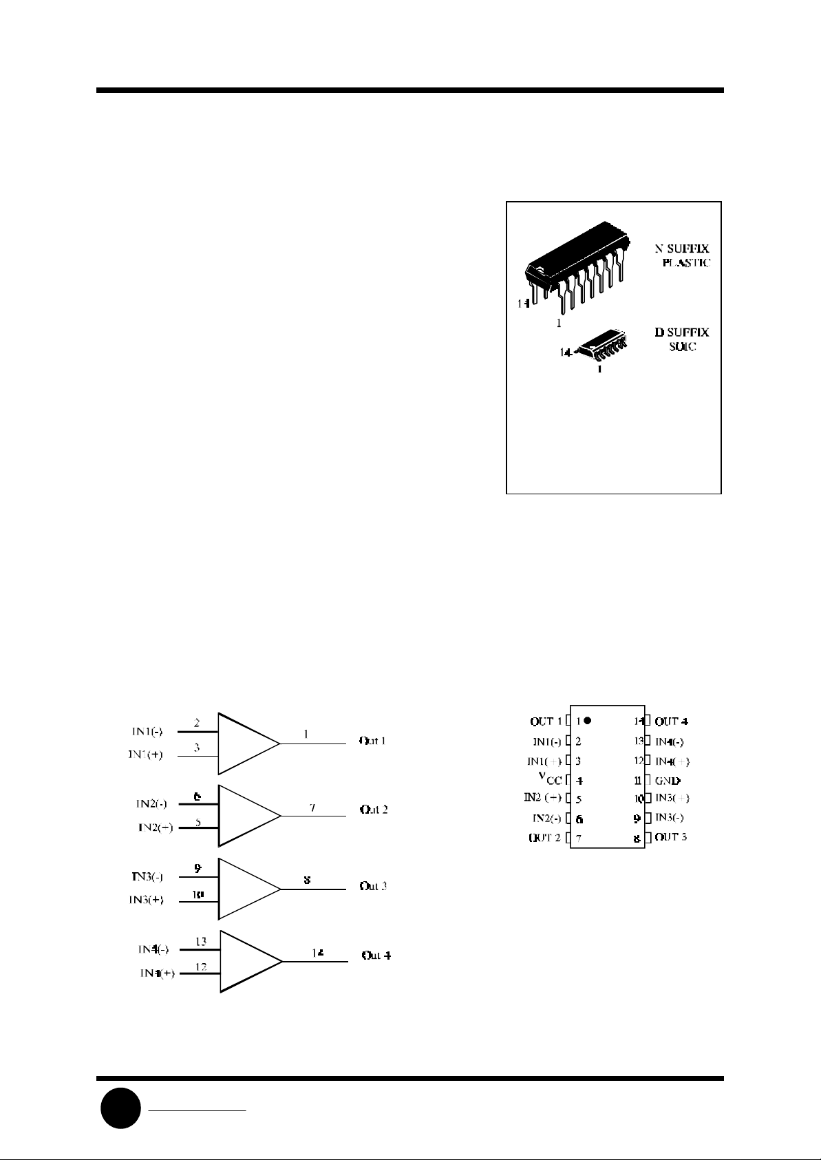
ORDERING INFORMATION
SL324N Plastic
SL324D SOIC
TA = 0° to 70° C
for all packages.
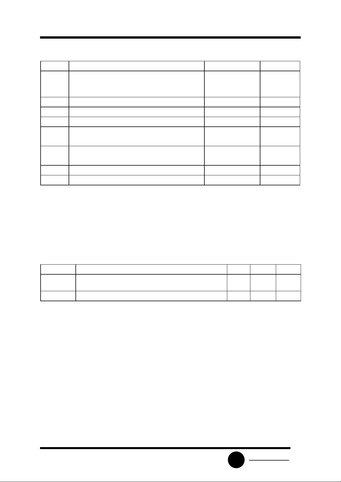
LOGIC DIAGRAM
PIN 4 = VCC
PIN 11= GND
PIN ASSIGNMENT
System Logic
SLS
Semiconductor
SL324
MAXIMUM RATINGS*
Symbol Parameter Value Unit
VCC Power Supply Voltages
Single Supply
Split Supplies
V
Input Differential Voltage Range (1) ±32 V
IDR
V
Input Common Mode Voltage Range -0.3 to 32 V
ICR
32
±16
ISC Output Short Circuit Duration Continuous
TJ Junction Temperature
Plastic Packages
Tstg Storage Temperature
Plastic Packages
150
-55 to +125
IIN Input Current, per pin (2) 50 mA
TL Lead Temperature, 1mm from Case for 10 Seconds 260 °C
*
Maximum Ratings are those values beyond which damage to the device may occur.
Functional operation should be restricted to the Recommended Operating Conditions.
+Derating - Plastic DIP: - 10 mW/°C from 65° to 125°C
SOIC Package: : - 7 mW/°C from 65° to 125°C
Notes:
1. Split Power Suppl ies.
2. VIN<-0.3V. This input current will only exist when voltage at any of the input leads is driven negative.
V
°C
°C
RECOMMENDED OPERATING CONDITIONS
Symbol Parameter Min Max Unit
VCC DC Supply Voltage ±2.5 or
5.0
TA Operating Temperature, All Pack age Types 0 +70 °C
This device contains protection circuitry to guard against damage due to high static voltages or electric
fields. However, precautions must be taken to avoid applications of any voltage higher than maximum rated
voltages to this high-impedance circuit. For proper operation, VIN and V
GND≤(VIN or V
OUT
)≤VCC.
should be constrained to the range
OUT
Unused inputs must always be tied to an appropriate logic voltage level (e.g., either GND or VCC).
Unused outputs must be left open.
±15 or
30
V
System Logic
SLS
Semiconductor
 Loading...