

SLS SL20T0081 Datasheet

SLS System Logic Semiconductor SL20T0081
81 COMMON x 132 SEGMENT STN LCD DRIVER / CONTROLLER
SL20T0081
SLS System Logic Semiconductor SL20T0081
DEVICE SPECIFICATION
OVERVIEW
INTRODUCTION
The SL20T0081 is a single-chip graphic dot-matrix liquid crystal display driver & controller that can be connected
directly to a microprocessor bus. 8-bit parallel or serial display data sent from the microprocessor is stored in the
internal display data RAM and the chip generates a liquid crystal drive signal independent of the micro-processor. The
SL20T0081 contains 81x132 bits of display data RAM and there is a 1-to-1 correspondence between the liquid crystal
panel pixels and the internal RAM bits, and the device contains 81 common output circuits and 132 segment output
circuits, so that a single chip can drive a 81x132dot display (capable of displaying 8 columns x5 rows of a 16 x 16 dot
font). Moreover, the capacity of the display can be extended through the use of master/ slave structures between chips.
The chips are able to minimize power consumption because no exte rnal operating clock is necessary for the display
data RAM read/write operation. Furthermore, because each chip is equipped internally with a low -power liquid crystal
driver power supply, resistors for liquid crystal driver power voltage adjustment and a display clock RC oscillator circuit,
the SL20T0081 Series chips can be used to create the lowest power display system with the fewest
components for high performance portable systems.
FEATURES
Direct display of RAM data through the display data RAM.
RAM capacity : 81x132 = 8580 bits
Table 1. Duty and Bias selection
Duty LCD Driver Bias Maximum display matrix
1/81 1/10 or 1/8 81 x 132
1/65 1/9 or 1/7 65 x 132
1/55 1/8 or 1/6 55 x 132
1/49 1/8 or 1/6 49 x 132
1/33 1/6 or 1/5 33 x 132
RAM bit data : “1” Non-illuminated
“0” illuminated
(during normal display)
High-speed 8-bit MPU interface
The chip can be connected directly to the both the 80x86 series MPUs and the 68000 series MPUs.
Serial interface available (supports write operation only).
Abundant command functions
Display data Read/Write,display ON/OFF, Normal/Reverse display mode, page address set, display start line set,
column address set, status read, display all point ON/OFF, LCD bias set, electronic volume, read/modify/write,
segment driver direction select, power saver, static indicator, common output status select, V5 voltage regulation
internal resistor ratio set.
Static drive circuit equipped internally for indicators
1 driver, with 4 kinds of flashing mode

SLS System Logic Semiconductor SL20T0081
Built-in Power Supply Circuit
Low-power liquid crystal display power supply circuit equipped inter nally.
Booster circuit (with Boost ratios of x2 / x3 / x4 / x5, where the step-up voltage reference power supply can be input
externally).
High-accuracy voltage adjustment circuit (Thermal gradient -0.05%/oC or external input).
LCD driver voltage regulator resistors and voltage followers equipped internally.
RC oscillator circuit equipped internally (external clock can also be selected).
Operating Voltage Range
Supply Voltage (VDD) : 2.4V ~ 3.6V
LCD driver Voltage (VLCD) : 4.5V ~ 16.0V
Low Power Consumption
Operating power : 40uA typical (conditions:V
supply ON,display OFF and normal mode is selected )
Standby power : 10uA maximum (during power save [standby] mode)
Operating Temperatures
Wide range of operating temperatures : -40 to 85oC
=3V, x 4 boosting (VCI = V
DD
), V0 =11V, Internal power
DD
CMOS Process
Package Type
TCP
SLS System Logic Semiconductor SL20T0081
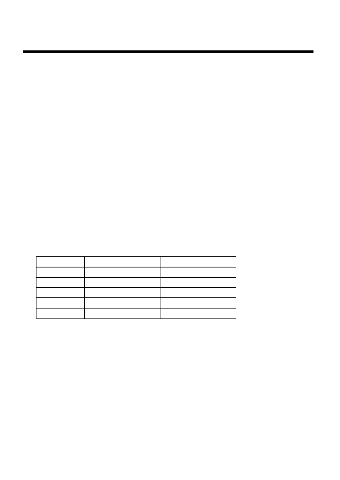
BLOCKDIAGRAM
VDD
VSS
V0
V1
V2
V3
V4
CAP1+
CAP1CAP2+
CAP2CAP3+
CAP4+
VOUT
VCI
VEXT
VR
IREF
IRE
HPMB
Power
Supply
Circuit
COM0
COM39
COM
Drivers
Display Data Read Circuit
Display Data Memory
Column Address Decoder
SEG0
81 x 132 bits
SEG Drivers
SEG131
Row Address Decoder
COM40
COM
Drivers
&
Timing Generation
Read/Write Circuit
COM79
COMS
COMS
Circuit
Oscillation
FR
FRS
SYNC
CL
DISP
MS
DUTY0
DUTY1
DUTY2
CLS
CE1
CE2
RS
RD (E)
WR (R/W)
Command Decoder
MPU Interface
PS
P68/86
RESET
D7 (SI)
D5
D6 (SCK)
Status
D4
D2
D1D3D0
SLS System Logic Semiconductor SL20T0081
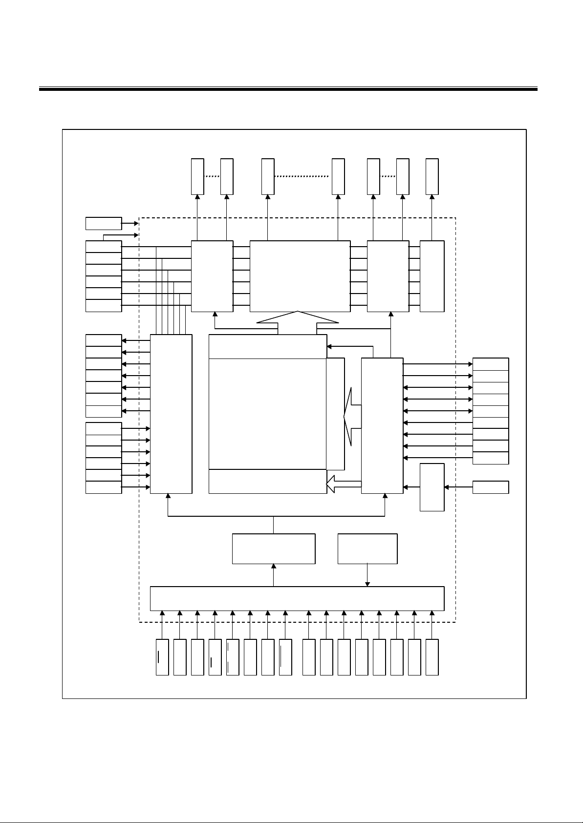
PAD CONFIGURATION
PAD Layout
Figure 1. SL20T0081 PAD Layout
282 147
283
325
Table 2. SL20T0081 PAD Dimensions
Item Pad No.
2 to10, 94 to 102, 104 to 146,
148 to 281, 283 to 325
11 to 41, 45-46, 50 to 93 80
Pad pitch
41-42, 44-45, 46-47, 49-50 110
42 to 44, 47 to 49 120
1-2, 102-103, 147-148, 281-282 131
10-11, 93-94 90
146
Y
X
(0,0)
104
1031
Size
Unit
X Y
8900 3000-Chip Size
60
µm
2 to 10, 94 to 102, 148 to 281 37 92
104 to 146, 283 to 325 92 37
Bumped PAD size
11 to 41, 45, 46, 50 to 93 57 92
(Bottom)
42 to 44, 47 to 49 67 92
1, 103, 147, 282 72 97
All PADBumped PAD height 18
Figure 2. Align Key Coordination
COG Align Key Coordination ILB Align Key Coordination Potting Mark Coordination
30µm
30µm 30µm
30µm
30µm 30µm
30µm 30µm 30µm
60µm
30µm
60µm 72µm
(-4230.0, -1415.0) (4230.0, -1430.0) upper left : (-4365.0, 1415.0) (4346.0, 1406.0)
lower right : (4365.0, -1415.0)
SLS System Logic Semiconductor SL20T0081
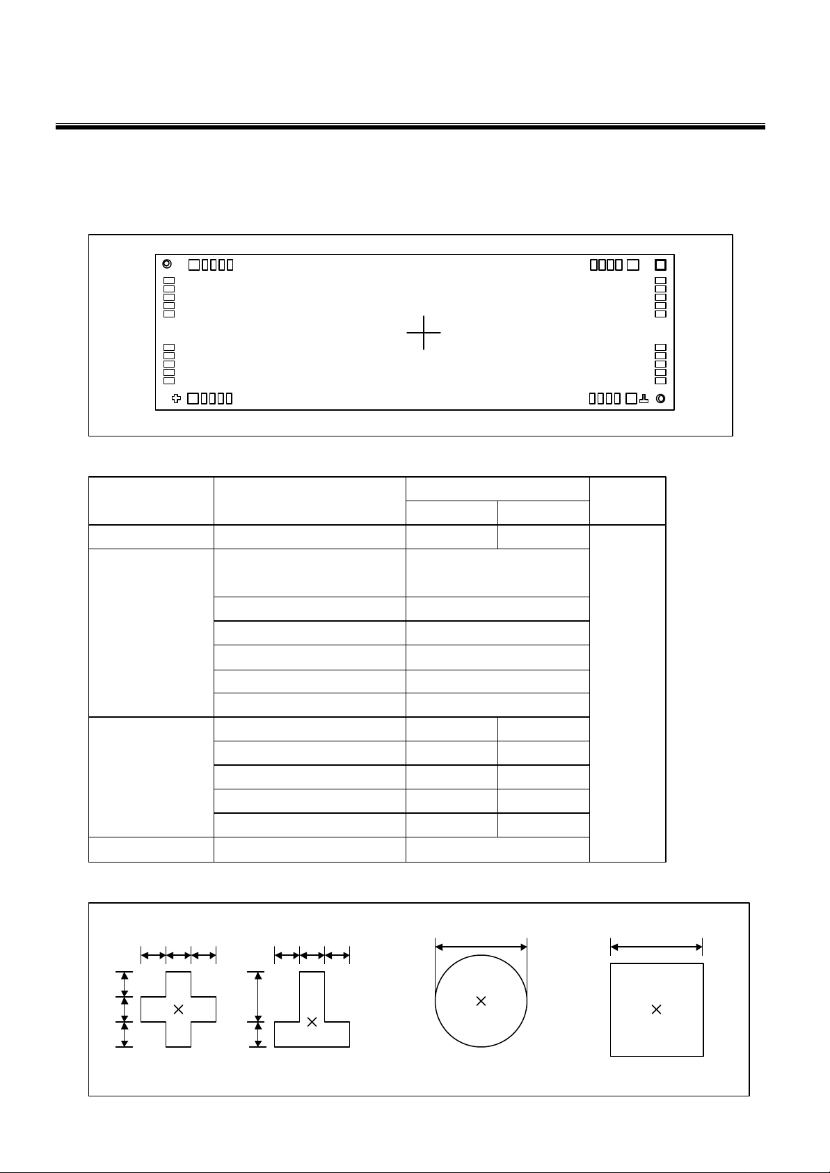
PAD CENTER COORDINATES
PAD PAD PAD PAD
No. name No. name
1 DUMMY5 -4121 -1411 57 CAP1- 540 -1411
2 DUMMY6 -3990 -1411 58 CAP1+ 620 -1411
3 DUMMY7 -3930 -1411 59 CAP1+ 700 -1411
4 DUMMY8 -3870 -1411 60 CAP2+ 780 -1411
5 DUMMY9 -3810 -1411 61 CAP2+ 860 -1411
6 DUMMY10 -3750 -1411 62 CAP2- 940 -1411
7 DUMMY11 -3690 -1411 63 CAP2- 1020 -1411
8 DUMMY12 -3630 -1411 64 VDD 1100 -1411
9 DUMMY13 -3570 -1411 65 VEXT 1180 -1411
10 DUMMY14 -3510 -1411 66 IREF 1260 -1411
11 FRS -3420 -1411 67 TEST_VREF 1340 -1411
12 FR -3340 -1411 68 VSS 1420 -1411
13 SYNC -3260 -1411 69 V1 1500 -1411
14 CL -3180 -1411 70 V1 1580 -1411
15 DISP -3100 -1411 71 V2 1660 -1411
16 VDD -3020 -1411 72 V2 1740 -1411
17 VSS -2940 -1411 73 V3 1820 -1411
18 CE1 -2860 -1411 74 V3 1900 -1411
19 CE2 -2780 -1411 75 V4 1980 -1411
20 VDD -2700 -1411 76 V4 2060 -1411
21 RESETB -2620 -1411 77 V0 2140 -1411
22 RS -2540 -1411 78 V0 2220 -1411
23 VSS -2460 -1411 79 VR 2300 -1411
24 WR(R/W) -2380 -1411 80 VR 2380 -1411
25 RD(E) -2300 -1411 81 VSS 2460 -1411
26 VDD -2220 -1411 82 VSS 2540 -1411
27 D<0> -2140 -1411 83 VDD 2620 -1411
28 D<1> -2060 -1411 84 MS 2700 -1411
29 D<2> -1980 -1411 85 CLS 2780 -1411
30 D<3> -1900 -1411 86 VSS 2860 -1411
31 D<4> -1820 -1411 87 P68/80 2940 -1411
32 D<5> -1740 -1411 88 PS 3020 -1411
33 D<6> -1660 -1411 89 VDD 3100 -1411
34 D<7> -1580 -1411 90 HPMB 3180 -1411
35 VSS -1500 -1411 91 VSS 3260 -1411
36 VDD -1420 -1411 92 IRE 3340 -1411
37 DUTY0 -1340 -1411 93 VDD 3420 -1411
38 DUTY1 -1260 -1411 94 TRCON 3510 -1411
39 VDD -1180 -1411 95 VSS 3570 -1411
40 VSS -1100 -1411 96 TRIM<4> 3630 -1411
41 DUTY2 -1020 -1411 97 TRIM<3> 3690 -1411
42 VDD -910 -1411 98 VSS 3750 -1411
43 VDD -790 -1411 99 TRIM<2> 3810 -1411
44 VDD -670 -1411 100 TRIM<1> 3870 -1411
45 VCI -560 -1411 101 VSS 3930 -1411
46 VCI -480 -1411 102 TRIM<0> 3990 -1411
47 VSS -370 -1411 103 DUMMY15 4121 -1411
48 VSS -250 -1411 104 DUMMY16 4361 -1250
49 VSS -130 -1411 105 COM<39> 4361 -1190
50 VOUT -20 -1411 106 COM<38> 4361 -1130
51 VOUT 60 -1411 107 COM<37> 4361 -1070
52 CAP4+ 140 -1411 108 COM<36> 4361 -1010
53 CAP4+ 220 -1411 109 COM<35> 4361 -950
54 CAP3+ 300 -1411 110 COM<34> 4361 -890
55 CAP3+ 380 -1411 111 COM<33> 4361 -830
56 CAP1- 460 -1411 112 COM<32> 4361 -770
X Y X Y

SLS System Logic Semiconductor SL20T0081
PAD CENTER COODINATES (continued)
PAD PAD PAD PAD
No. name No. name
113 COM<31> 4361 -710 169 SEG<20> 2730 1411
114 COM<30> 4361 -650 170 SEG<21> 2670 1411
115 COM<29> 4361 -590 171 SEG<22> 2610 1411
116 COM<28> 4361 -530 172 SEG<23> 2550 1411
117 COM<27> 4361 -470 173 SEG<24> 2490 1411
118 COM<26> 4361 -410 174 SEG<25> 2430 1411
119 COM<25> 4361 -350 175 SEG<26> 2370 1411
120 COM<24> 4361 -290 176 SEG<27> 2310 1411
121 COM<23> 4361 -230 177 SEG<28> 2250 1411
122 COM<22> 4361 -170 178 SEG<29> 2190 1411
123 COM<21> 4361 -110 179 SEG<30> 2130 1411
124 COM<20> 4361 -50 180 SEG<31> 2070 1411
125 COM<19> 4361 10 181 SEG<32> 2010 1411
126 COM<18> 4361 70 182 SEG<33> 1950 1411
127 COM<17> 4361 130 183 SEG<34> 1890 1411
128 COM<16> 4361 190 184 SEG<35> 1830 1411
129 COM<15> 4361 250 185 SEG<36> 1770 1411
130 COM<14> 4361 310 186 SEG<37> 1710 1411
131 COM<13> 4361 370 187 SEG<38> 1650 1411
132 COM<12> 4361 430 188 SEG<39> 1590 1411
133 COM<11> 4361 490 189 SEG<40> 1530 1411
134 COM<10> 4361 550 190 SEG<41> 1470 1411
135 COM<9> 4361 610 191 SEG<42> 1410 1411
136 COM<8> 4361 670 192 SEG<43> 1350 1411
137 COM<7> 4361 730 193 SEG<44> 1290 1411
138 COM<6> 4361 790 194 SEG<45> 1230 1411
139 COM<5> 4361 850 195 SEG<46> 1170 1411
140 COM<4> 4361 910 196 SEG<47> 1110 1411
141 COM<3> 4361 970 197 SEG<48> 1050 1411
142 COM<2> 4361 1030 198 SEG<49> 990 1411
143 COM<1> 4361 1090 199 SEG<50> 930 1411
144 COM<0> 4361 1150 200 SEG<51> 870 1411
145 COMSR 4361 1210 201 SEG<52> 810 1411
146 DUMMY17 4361 1270 202 SEG<53> 750 1411
147 DUMMY18 4121 1411 203 SEG<54> 690 1411
148 DUMMY19 3990 1411 204 SEG<55> 630 1411
149 SEG<0> 3930 1411 205 SEG<56> 570 1411
150 SEG<1> 3870 1411 206 SEG<57> 510 1411
151 SEG<2> 3810 1411 207 SEG<58> 450 1411
152 SEG<3> 3750 1411 208 SEG<59> 390 1411
153 SEG<4> 3690 1411 209 SEG<60> 330 1411
154 SEG<5> 3630 1411 210 SEG<61> 270 1411
155 SEG<6> 3570 1411 211 SEG<62> 210 1411
156 SEG<7> 3510 1411 212 SEG<63> 150 1411
157 SEG<8> 3450 1411 213 SEG<64> 90 1411
158 SEG<9> 3390 1411 214 SEG<65> 30 1411
159 SEG<10> 3330 1411 215 SEG<66> -30 1411
160 SEG<11> 3270 1411 216 SEG<67> -90 1411
161 SEG<12> 3210 1411 217 SEG<68> -150 1411
162 SEG<13> 3150 1411 218 SEG<69> -210 1411
163 SEG<14> 3090 1411 219 SEG<70> -270 1411
164 SEG<15> 3030 1411 220 SEG<71> -330 1411
165 SEG<16> 2970 1411 221 SEG<72> -390 1411
166 SEG<17> 2910 1411 222 SEG<73> -450 1411
167 SEG<18> 2850 1411 223 SEG<74> -510 1411
168 SEG<19> 2790 1411 224 SEG<75> -570 1411
X Y X Y

SLS System Logic Semiconductor SL20T0081
PAD CENTER COODINATES (continued)
PAD PAD PAD PAD
No. name No. name
225 SEG<76> -630 1411 281 DUMMY1 -3990 1411
226 SEG<77> -690 1411 282 DUMMY2 -4121 1411
227 SEG<78> -750 1411 283 DUMMY3 -4361 1270
228 SEG<79> -810 1411 284 COM<40> -4361 1210
229 SEG<80> -870 1411 285 COM<41> -4361 1150
230 SEG<81> -930 1411 286 COM<42> -4361 1090
231 SEG<82> -990 1411 287 COM<43> -4361 1030
232 SEG<83> -1050 1411 288 COM<44> -4361 970
233 SEG<84> -1110 1411 289 COM<45> -4361 910
234 SEG<85> -1170 1411 290 COM<46> -4361 850
235 SEG<86> -1230 1411 291 COM<47> -4361 790
236 SEG<87> -1290 1411 292 COM<48> -4361 730
237 SEG<88> -1350 1411 293 COM<49> -4361 670
238 SEG<89> -1410 1411 294 COM<50> -4361 610
239 SEG<90> -1470 1411 295 COM<51> -4361 550
240 SEG<91> -1530 1411 296 COM<52> -4361 490
241 SEG<92> -1590 1411 297 COM<53> -4361 430
242 SEG<93> -1650 1411 298 COM<54> -4361 370
243 SEG<94> -1710 1411 299 COM<55> -4361 310
244 SEG<95> -1770 1411 300 COM<56> -4361 250
245 SEG<96> -1830 1411 301 COM<57> -4361 190
246 SEG<97> -1890 1411 302 COM<58> -4361 130
247 SEG<98> -1950 1411 303 COM<59> -4361 70
248 SEG<99> -2010 1411 304 COM<60> -4361 10
249 SEG<100> -2070 1411 305 COM<61> -4361 -50
250 SEG<101> -2130 1411 306 COM<62> -4361 -110
251 SEG<102> -2190 1411 307 COM<63> -4361 -170
252 SEG<103> -2250 1411 308 COM<64> -4361 -230
253 SEG<104> -2310 1411 309 COM<65> -4361 -290
254 SEG<105> -2370 1411 310 COM<66> -4361 -350
255 SEG<106> -2430 1411 311 COM<67> -4361 -410
256 SEG<107> -2490 1411 312 COM<68> -4361 -470
257 SEG<108> -2550 1411 313 COM<69> -4361 -530
258 SEG<109> -2610 1411 314 COM<70> -4361 -590
259 SEG<110> -2670 1411 315 COM<71> -4361 -650
260 SEG<111> -2730 1411 316 COM<72> -4361 -710
261 SEG<112> -2790 1411 317 COM<73> -4361 -770
262 SEG<113> -2850 1411 318 COM<74> -4361 -830
263 SEG<114> -2910 1411 319 COM<75> -4361 -890
264 SEG<115> -2970 1411 320 COM<76> -4361 -950
265 SEG<116> -3030 1411 321 COM<77> -4361 -1010
266 SEG<117> -3090 1411 322 COM<78> -4361 -1070
267 SEG<118> -3150 1411 323 COM<79> -4361 -1130
268 SEG<119> -3210 1411 324 COMSL -4361 -1190
269 SEG<120> -3270 1411 325 DUMMY4 -4361 -1250
270 SEG<121> -3330 1411
271 SEG<122> -3390 1411
272 SEG<123> -3450 1411
273 SEG<124> -3510 1411
274 SEG<125> -3570 1411
275 SEG<126> -3630 1411
276 SEG<127> -3690 1411
277 SEG<128> -3750 1411
278 SEG<129> -3810 1411
279 SEG<130> -3870 1411
280 SEG<131> -3930 1411
X Y X Y
SLS System Logic Semiconductor SL20T0081
PIN DESCRIPTION
Power Supply Pins
Pin Name I/O Function
VDD
VSS
VCI
V0
V1
V2
V3
V4
Power
Supply
Power
Supply
Power
Supply
Power
Supply
Positive Power Supply.
System Ground.
Voltage Booster input pin. The power supply for the voltage booster. VCI input voltage
is the reference of boosted output voltage (VOUT) of voltage booster.
LCD driver supply voltage pins.
When the internal LCD power supply circuit is enabled, these voltages are generated by it.
When the internal LCD power supply circuit is disabled, these voltages must be supplied
externally, and they should have the following relationship.
VSS < V4 < V3 < V2 < V1 < V0
LCD Power Supply Circuit Pins
Pin Name I/O Function
CAP1+ O Voltage booster pin. Connect a capacitor between this pin and the CAP1- pin
CAP1- O Voltage booster pin. Connect a capacitor between this pin and the CAP1+ pin
CAP2+ O Voltage booster pin. Connect a capacitor between this pin and the CAP2- pin
CAP2- O Voltage booster pin. Connect a capacitor between this pin and the CAP2+ pin
CAP3+ O Voltage booster pin. (refer the application example to connecting a capacitor)
CAP4+ O Voltage booster pin. (refer the application example to connecting a capacitor)
VOUT O
VEXT I
IREF I
VR I
IRE I
Voltage booster pin. Connect a capacitor between this pin and VSS.
This is the external reference voltage input pin of the LCD power supply circuit.
This pin is valid only when internal reference voltage circuit is disabled (IREF=0).
Internal reference voltage circuit enable pin.
IREF = 0 : Internal reference voltage circuit is disabled. External reference voltage is
inputted via VEXT pin.
IREF = 1 : Internal reference voltage circuit is enabled.
External V0 voltage adjustment pin.
VR pin is valid only when the internal voltage regulator resistors are not used (IRE=0)
Internal voltage regulator resistor enable pin.
This pin selects the resistors for the V0 voltage level adjustme nt.
IRE = 1 : Use the internal resistors
IRE = 0 : Do not use the internal resistors. The V0 voltage level is controlled by the
external resisters that connected among V0 pin and VR pin and VSS.

SLS System Logic Semiconductor SL20T0081
System Control pins
Pin Name I/O Function
This pin selects the master/slave operation for the SL20T0081chip. Master operation
outputs the timing signals that are required for the LCD display, while slave operation
inputs the timing signals required for the liquid crystal display.
MS = 1 : Master operation
MS = 0 : Slave operation
Following table shows difference of the master operation and the slave operation.
MS I
MS
CLS
Internal Oscillator
Circuit
Internal Power
Supply Circuit
CL
SYNC DISP
CL I/O
CLS I
SYNC I/O
DISP I/O
DUTY0
DUTY1
DUTY2
1
0 Disabled-
This is the display clock input/output pin.
When multiple SL20T0081 chips are used in master/slave mode, all of CL pins must be
connected each other.
Internal RC oscillator enable pin.
CLS = 1 : Internal oscillator circuit is enabled.
CLS = 0 : Internal oscillator circuit is disabled.
When CLS=0, the display clock must be inputted through the CL pi n.
This pin is valid only when SL20T0081operating in master operation.
LCD synchronization signal input/output pin.
When multiple SL20T0081 chips are used in master/slave mode, all of SYNC pins must be
connected each other.
This is the liquid crystal display blanking control pin.
When multiple SL20T0081 chips are used in master/slave mode, all of DISP pins must be
connected each other.
The LCD driver duty ratio selection pins.
DUTY2
I
1
0
1
0
0
0
0
Enabled
Disabled
DUTY1
1 1 1/811
0
1
1
0
0 0 1/33
DUTY0
0
1
0
1
Enabled
Enabled
Disabled Input Input Input
Duty ratio
1/81
1/65
1/55
1/49
Output
Input
Output
Output
Common Output
Even, Odd
normal
Output
Output
“
“
“
“
HPMB I
When Duty = (1, 1, 1), 1/81 duty ratio is selected, and common output pin configuration is
changed. At this mode, all even numbered common output pins are outputting right side of
the device and all odd numbered common output pins are outputting left side of the
device.
This is the power control pin for the power supply circuit for liquid crystal drive.
HPMB = 1 : Normal mode
HPMB = 0 : High power mode
This pin is enabled only when the master operation mode is selected.
It is fixed to either 0 or 1 when the slave operation mode is selected.

SLS System Logic Semiconductor SL20T0081
System Interface pins
Pin Name I/O Function
RESET I
D7 ~ D0
(SI)
(SCK)
RS I
CE1
CE2
RD
(E)
WR
(R/W)
I/O
Device Reset pin.
When RESET = 0, device initialization operation is executed.
8bit bi-directional data bus that should be connected to the standard MPU data bus.
When PS=0 the serial interface is enabled and pins are set as following.
D7 : Serial data input (SI)
D6 : Serial interface clock input (SCK)
D5 ~ D0 : high impedance state
When the chip does not be selected, D7 ~ D0 are set to high impedance.
Display data / Control data selection signal input pin
RS = 1 : D7 ~ D0 input are display data
RS = 0 : D7 ~ D0 input are control data
Chip Select signal input pins
I
I
I
When CE1 = 0 and CE2 = 1, then the chip select becomes active,
and data/command I/O is enabled.
• When the device connected to an 8080 MPU bus, this pin acts as “active LOW” read
signal input pin. If the device is selected and RD = 0, then SL20T0081outputs the data
to data bus pins.
• When the device connected to a 6800 MPU bus, this pin acts as “active HIGH”R/W
enable signal input pin. If the device is selected and RD = 1, then SL20T0081 executes
read or write operation that controlled by WR signal.
• When the device connected to an 8080 MPU bus, this pin acts as “active LOW” write
signal input pin. If the device is selected and WR = 0, then SL20T0081accepts the data
via data bus pins.
• When the device connected to a 6800 MPU bus, this pin acts as read/write control signal
input pin.
WR(R/W) = 1 : Read
WR(R/W) = 0 : Write
P68/80 I
PS I
Bus type selection pin.
P68/80 = 1 : 6800 MPU bus type interface.
P68/80 = 0 : 8080 MPU bus type interface
Parallel data transfer / Serial data transfer mode selection pin.
PS = 1 : Parallel data transfer mode.
PS = 0 : Serial data transfer mode.
PS Data transfer mode Data busRead SCK pinWrite
1 Parallel data transfer D7 ~D0enabled -enabled
0 Serial data transfer D7 (SI)disabled D6 (SCK)enabled
When PS = 0, RD(E) and WR(R/W) pins are fixed to either 0 or 1.

SLS System Logic Semiconductor SL20T0081
Liquid Crystal Drive Pins
Pin Name I/O Function
LCD segment driver output pins.
Segment driver output voltage is controlled by display data and FR signal.
SEG0
~
SEG131
COM0
~
COM79
COMS(R)
COMS(L)
FR O Static segment driver output pin. This pin is paired with FRS pin.
O
O
O
Display data FR
1 1 V0 V2
1 0 VSS V3
0 1 V2 V0
0 0 V3 VSS
Power save VSS
LCD common driver output pins.
Common driver output voltage is controlled by internal scanning data and FR signal.
Scan Data
1
1 0
0 1
0 0
Power save mode
Common drive output for the icons. There are two COMS pin, COMS(R), COMS(L).
They output same signal. When in master/slave mode, the same signal is output by both
master and slave.
FR
1
Segment driver output voltage
Normal Display Reverse Display
Common driver output voltage
VSS
V0
V1
V4
VSS
FRS O Static segment driver output pin. This pin is paired with FR pin.

SLS System Logic Semiconductor SL20T0081
FUNCTION DESCRIPTION
MICROPROCESSOR INTERFACE
Chip Select Input
There are CE1 and CE2 pins for chip selection. The SL20T0081can interface with an MPU only when CE1 is “L” and
CE2 is “H”. When these pins are set to any other combination, RS, RDB(E) and_WRB(RW) inputs are disabled and
D0to D7 are to be high impedance. And, in case of serial interface, the internal shift register and the counter are reset.
Parallel / Serial Interface
SL20T0081 has three types of interface with an MPU, which are one serial and two parallel interfaces. This parallel or
serial inter face is determined by PS pin.
Table 3. Parallel / Serial Interface Mode
PS Type CE1 P68/80 Interface mode
L Serial CE1 CE2
Parallel Interface (PS = “H”)
The 8-bit bi-directional data bus is used in parallel interface and the type of MPU is selected by P68/80 as shown
in table 4. The type of data transfer is determined by signals at RS, RD(E) and WR(R/W) as shown in table 5.
Table 4. Microprocessor Selection for Parallel Interface
P68/80 CE1 CE2 RS RD(E) WR(R/W) D0 to D7 MPU bus
H CE1 CE2 RS E R/W D0 to D7 6800-series
L CE1 CE2 RS RD WR D0 to D7 8080-series
Table 5. Parallel Data Transfer
Common 6800-series 8080-series
RS
RD
(E)
WR
(R/W)
RD WR
CE2
CE2CE1ParallelH
H
L 8080-series MPU mode
*
x Serial-mode
6800-series MPU mode
Description
*
x :Don’t care
H H H L H
H H L H L
L
L
H
H
H
L
L
H
Display data read out
Display data write
H
L
Writes to internal register (instruction)
Register status read
SLS System Logic Semiconductor SL20T0081
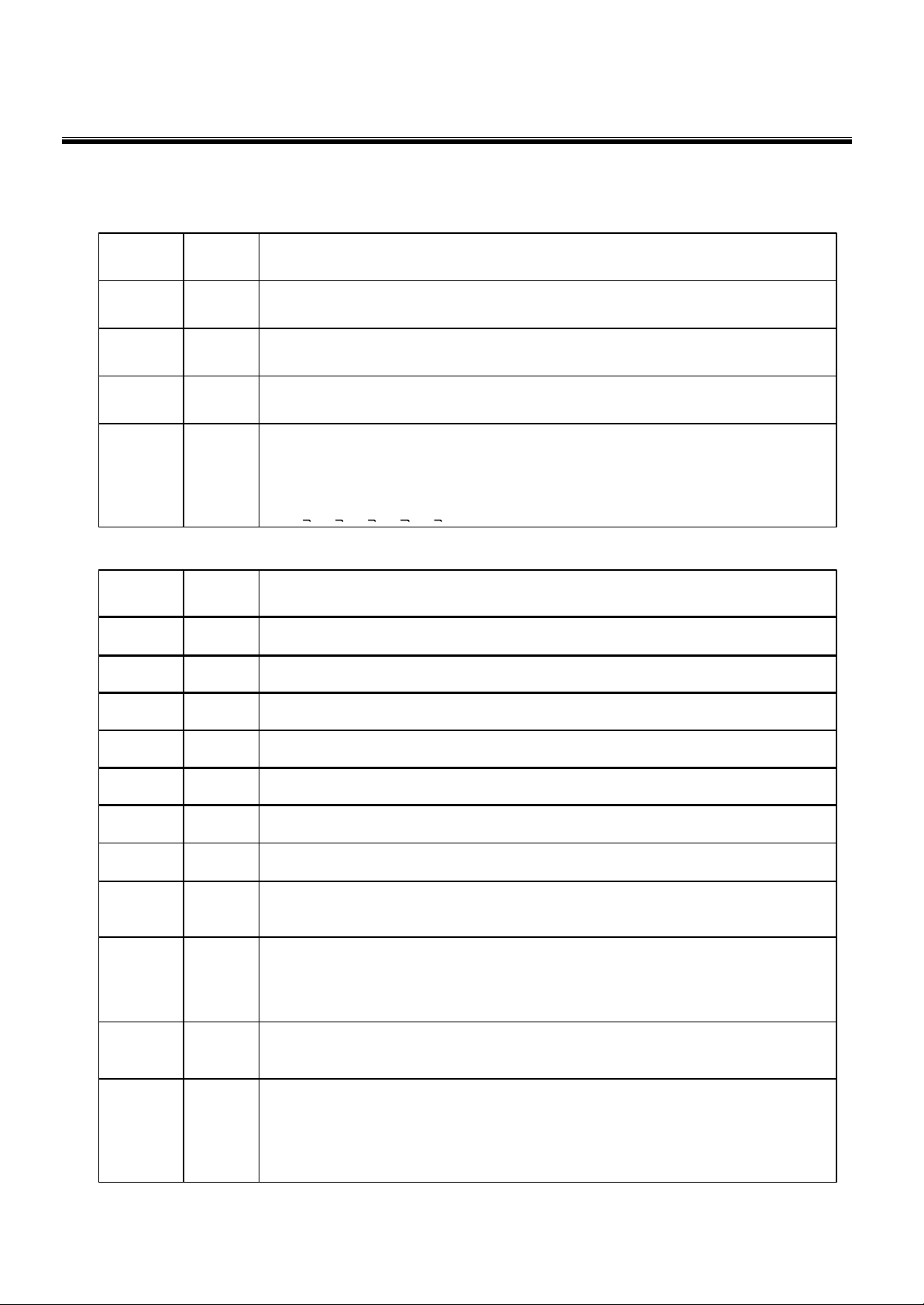
Serial Interface (PS = “L”)
When the SL20T0081 is active, serial data (D7) and serial clock (D6) input are enabled. And not active,the internal
8-bit shift register and the 3-bit counter are reset. Serial data can be read on the rising edge of serial clock going into
D6 and processed as 8-bit parallel data on the eighth serial clock. Serial data input is display data when RS is high
and caused by the line length, the operation check on the actual machine is recommended.
Figure 3. Serial Interface Timing
CE1
CE2
SID
SCLK
RS
Busy Flag
The Busy Flag indicates whether the SL20T0081 is operating or not. When D7 is “H” in read status operation, this
device is in busy status and will accept only read status instruction. If the cycle time is correct, the microprocessor
needs not to check this flag before each instruction, which improves the MPU performance.
D7 D6 D5 D4 D3 D2 D1 D0 D7 D6 D5 D4

SLS System Logic Semiconductor SL20T0081
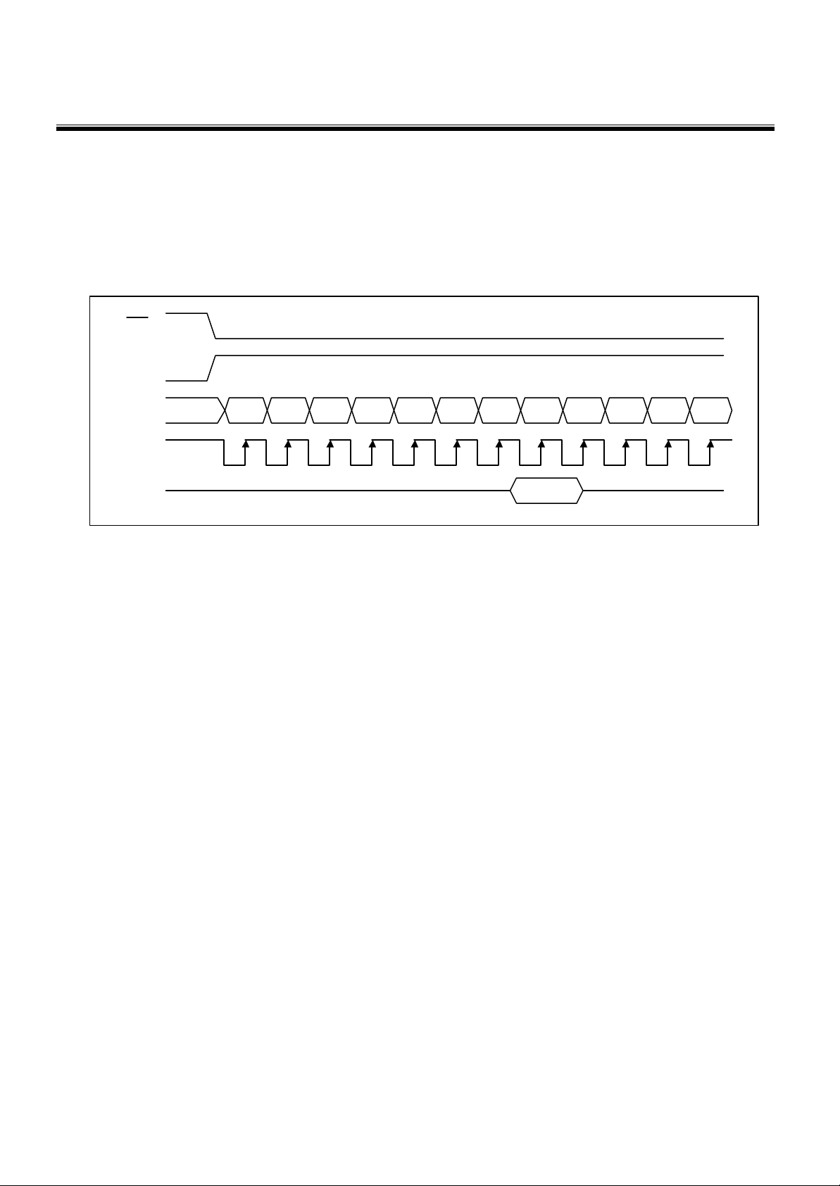
Data Transfer
The SL20T0081 used bus holder and internal data bus for data transfer with the MPU. When writing data from the
MPU to internal RAM, data is automatically transferred the bus holder to the RAM as shown in figure 4. And when
reading data from internal RAM to the MPU, the data for the init ial read cycle is stored in the bus holder (dummy read)
and the MPU reads this stored data from bus holder for the next data read cycle as shown in figure 5. This means
that a dummy read cycle must be inserted between each pair of address sets when a sequence of address sets is
executed. Therefore, the data of the specified address cannot be output with the read display data instruction right
after the address sets, but can be output at the second read of data.
Figure 4. Write Timing
MPU signals
RS
WR
D7 ~ D0
Internal signals
WR
BUS HOLDER
COLUMN ADDRESS
N D(N) D(N+1) D(N+2) D(N+3)
N D(N) D(N+1) D(N+2) D(N+3)
N N+1 N+2 N+3
N+4
SLS System Logic Semiconductor SL20T0081
Figure 5. Read Timing
MPU signals
RS
WR
RD
D7 ~ D0
Internal signals
WR
RD
BUS HOLDER
COLUMN ADDRESS
N Dummy D(N) D(N+1) D(N+2)
N D(N) D(N+1) D(N+2) D(N+3)
N N+1 N+2 N+3
N+4

SLS System Logic Semiconductor SL20T0081
LCD DISPLAY CIRCUIT
Display Data RAM
The Display Data RAM stores pixel data for the LCD. It is 81-row by 132-column addressable array. Each pixel
can be selected when the page and column addresses are specified. The 81 row are divided into 10 pages of 8 lines
and the 11th page with a single line (D0 only). Data is read from or written to the 8 lines of each page directly through
D7 to D0. The display data of D7 to D0 from the microprocessor correspond to the LCD common lines as shown in
figure 6. The microprocessor can read from and write to RAM through the I/O buffer. Since the LCD controller
operates independently, data can be written into RAM at the same time as data is being displayed without causing the
LCD flicker.
Figure 6. Display Data RAM to LCD panel Data Transfer
0 0 1 1 1
DB0
1 0 0 0 0
DB1
0 0 1 0 0
DB2
0 1 0 0 1
DB3
1 0 0 1 1
DB4
Display Data RAM LCD panel
Page Address Circuit
This circuit is for providing a Page Address to Display Data RAM show in figure 6. It incorporates 4-bit Page Address
register changed by only the “Set Page ”instruction. Page Address 11 is a special RAM area for the icons and display
dataD0 is only valid. When Page Address is above 8, it is imposs ible to access to Display Data RAM.
Line Address Circuit
This circuit assigns Display Data RAM a Line Address correspond ing to the first line (COM0) of the display. Therefore,
by setting Line Address repeatedly, it is possible to realize th e screen scrolling and page switching without changing
the contents of Display Data RAM as shown in figure 6. It incorporates 7-bit line address register changed by only the
initial display line instruction and 7-bit counter circuit. At the beginning of each LCD frame, the contents of register are
copied to the line counter which is increased by CL signal and generates the Line Address for transferring the 132-bit
RAM data to the display data latch circuit. However, display dat a of icons are not scrolled because the MPU can not
access Line Address of icons.
0
0
1
0
0
COM0
COM1
COM2
COM3
COM4
 Loading...