

Page 1

查询CX74063-26供应商
DATA SHEET
CX74063-26: RF Transceiver for Multi-Band GSM, GPRS, and
EDGE Applications with Power Ramping Controller and
Integrated Crystal Oscillator with 26 MHz Output
APPLICATIONS
• GSM850, EGSM900, DCS1800, and PCS1900 handsets
• GPRS handsets and modules
• EDGE downlink support
FEATURES
• Direct down-conversion receiver eliminates the external
image reject/IF filters
• Three separate LNAs with single-ended inputs
• RF gain range: GSM = 20 dB, DCS = 22 dB,
PCS = 20 dB. Baseband gain range = 100 dB
• Gain selectable in 2 dB steps
• Integrated receive baseband filters with tunable bandwidth
• Integrated DC offset correction sequencer
• Reduced filtering requirements with translational loop
transmit architecture
• Integrated transmit VCOs
• Wide RF range for quad band operation
• Integrated PAC loop
• Single integrated, fully programmable fractional-N
synthesizer suitable for multi-slot GPRS operation
• Fully integrated wideband Ultra High Frequency (UHF) VCO
• Integrated crystal oscillator
• Separate enable lines for power management transmit,
receive, and synthesizer modes
• Supply voltage down to 2.6 V
• Band select and front-end enable states may be exercised
on output pins to control external circuitry
• Low external component count
• Optional bypass of baseband filtering for use with high
dynamic range Analog to Digital Converters (ADCs) for
current savings
• Interfaces to low dynamic range ADC
• Meets AM suppression requirements without baseband
interaction
• 56-pin RFLGA 8x8 mm package
• Low power standby mode
DESCRIPTION
The CX74063-26 transceiver is a highly integrated device for
multi-band Global System for Mobile Communications™
(GSM™) or General Packet Radio Service (GPRS) applications.
The device requires a minimal number of external components
to complete a GSM radio subsystem. The CX74063-26
supports GSM850, EGSM900, DCS1800, and PCS1900
applications. The receiver also supports downlink Enhanced
Data-Rate GSM Evolution (EDGE).
The receive path implements a direct down-conversion
architecture that eliminates the need for Intermediate
Frequency (IF) components. The CX74063-26 receiver consists
of three integrated Low Noise Amplifiers (LNAs), a quadrature
demodulator, tunable receiver baseband filters, and a
DC-offset correction sequencer.
In the transmit path, the device consists of an In-phase and
Quadrature (I/Q) modulator within a frequency translation loop
designed to perform frequency up-conversion with high output
spectral purity. This loop also contains a phase-frequency
detector, charge pump, mixer, programmable dividers, and
high power transmit Voltage Controlled Oscillators (VCOs) with
no external tank required. With the integrated gain controller
(and an integrator ), the device realizes the Power Amplifier
Control (PAC) functionality when combined with a coupler, a
Radio Frequency (RF) detector and a Power Amplifier (PA).
The CX74063-26 also features an integrated, fully
programmable, sigma-delta fractional-N synthesizer suitable
for GPRS multi-slot operation. Except for the loop filter, the
frequency synthesizer function, including a wideband VCO, is
completely on-chip. The reference frequency for the
synthesizer is supplied by the integrated crystal oscillator
circuitry.
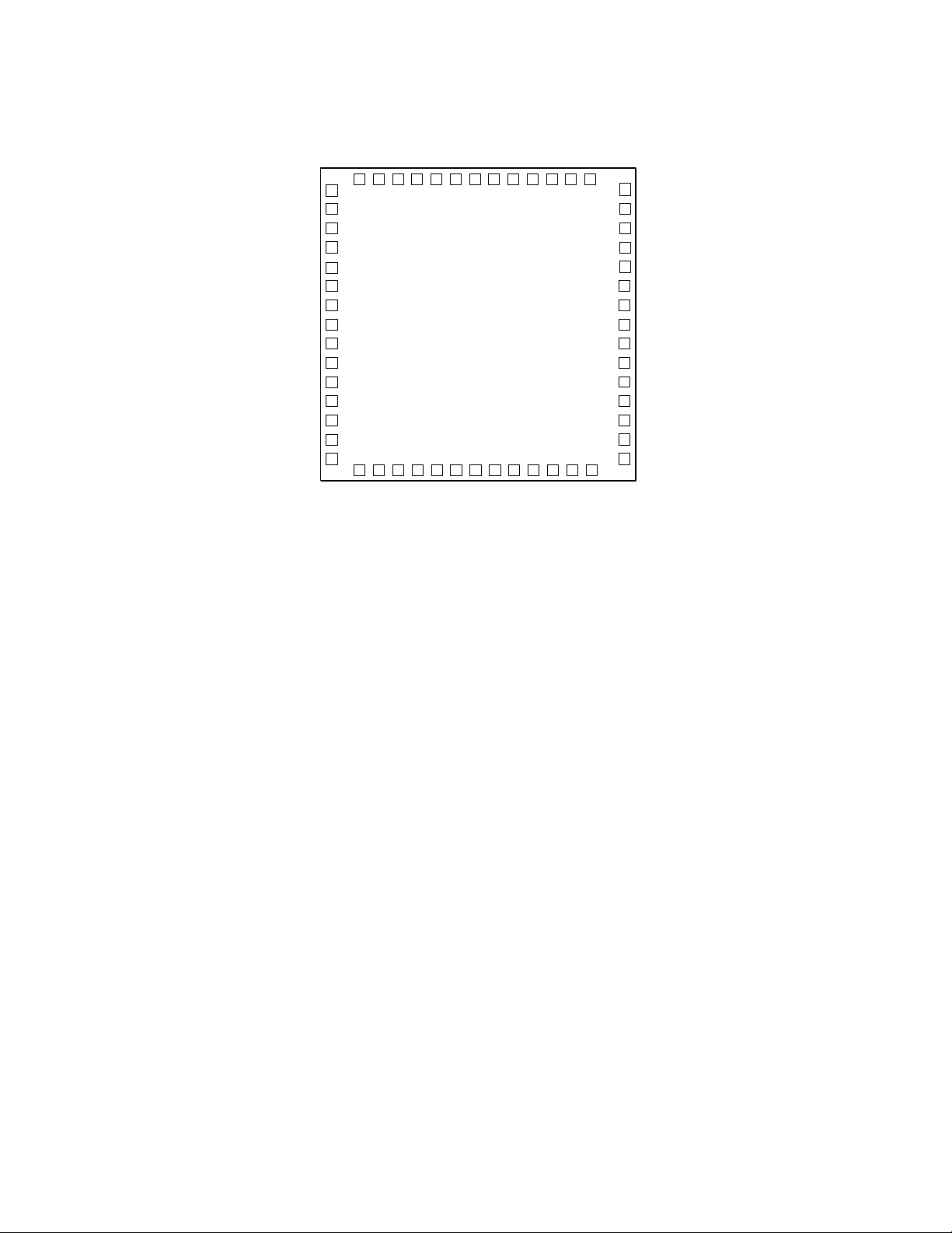
The 56-pin 8x8 RF Land Grid Array (RFLGA™) device package
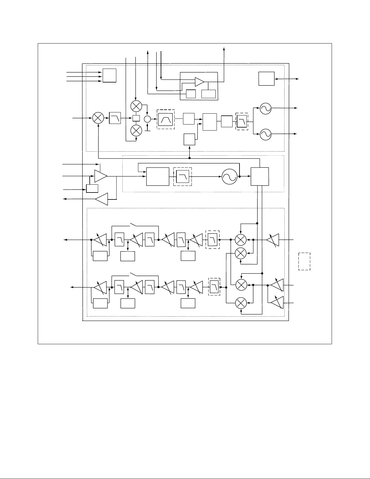
and pin configuration are shown in Figure 1. A functional block
diagram is shown in Figure 2. Signal pin assignments,
functional pin descriptions, and equivalent circuitry are
provided in Table 1.
Skyworks Solutions, Inc., Proprietary and Confidential 1
103052A [781] 376-3000 I FAX [781] 376-3100 I SALES@SKYWORKSINC.COM I WWW.SKYWORKSINC.COM MAY 16, 2003
Page 2
Data Sheet I CX74063-26
RXENA
TXENA
PCO
VCXO_EN
PDETVCC
VCC1
TXCPO
TXINP
LNA900IN
GNDLNA900
LNA1800IN
PDET
LNA1900IN
UHFBYP
UHFTUNE
VCCUHF
VCC3
RXQN
RXQP
RXIN
RXIP
VCC4
VCCTXVCO
TX900
TX1800/TX1900
TXVCO TUNE
VDDBB
CAPQP
44
28
CAPQN
43
LE
42
CLK
41
40
DATA
39
XTALTUNE
38
SXENA
37
VCCFN_CP
36
UHFCPO
GNDFN
35
34
XTAL
33
VCCF
32
VCCD
31
GNDD
30
XTALBUF
29
LPFADJ
C1328
1
56
545355
52
504951
48
24
VCC2
CAPIP
464547
262725
CAPIN
2
3
4
5
6
7
8
9
10
11
12
13
14
NC
16
181917
20
TXQP
TXQN
222321
TXIFP
TXIFN
15
NC
TXIP
PAVAPC
TXIN
BBVAPC
Figure 1. CX74063-26 Pinout – 56-Pin RFLGA (8 x 8 mm) (Top View)
2 Skyworks Solutions, Inc., Proprietary and Confidential
MAY 16, 2003 [781] 376-3000 I FAX [781] 376-3100 I SALES@SKYWORKSINC.COM I WWW.SKYWORKSINC.COM 103052A
Page 3
DATA
CLK
LE
TXINP
Tx PATH
TXIN
TXIP
TXQN
TXQP
+
FILTN
FILTP
PDET
PDETVCC
BBVAPC
PA GAIN CONTROLLER
+
–
DET
OFFSET
TxIFP
TxIFN
VCC
GEN
D2
D1
PFD
PAVAPC
CP
TXCPO
Data Sheet I CX74063-26
PCO
GSM850/EGSM900
TX900
TXVCOTUNE
TX1800/TX1900
DCS1800/PCS1900
VCXO_EN
XTAL
XTALTUNE
XTALBUF
RXIP
RXIN
RXQP
RXQN
VGA2
VGA2
DCOC
DCOC
DCOC
DCOC
Frac-N
UHFCPO
DCOC
DCOC
VGA1
VGA1
UHFTUNE
CAPIP
CAPIN
CAPQP
CAPQN
LO
Rx PATH
GSM
LNA
DCS
LNA
PCS
LNA
Sx
LNA900IN
Indicates
Off-chip
LNA1800IN
LNA1900IN
C900
Figure 2. CX74063-26 Transceiver Block Diagram
Skyworks Solutions, Inc., Proprietary and Confidential 3
103052A [781] 376-3000 I FAX [781] 376-3100 I SALES@SKYWORKSINC.COM I WWW.SKYWORKSINC.COM MAY 16, 2003
Page 4
Data Sheet I CX74063-26
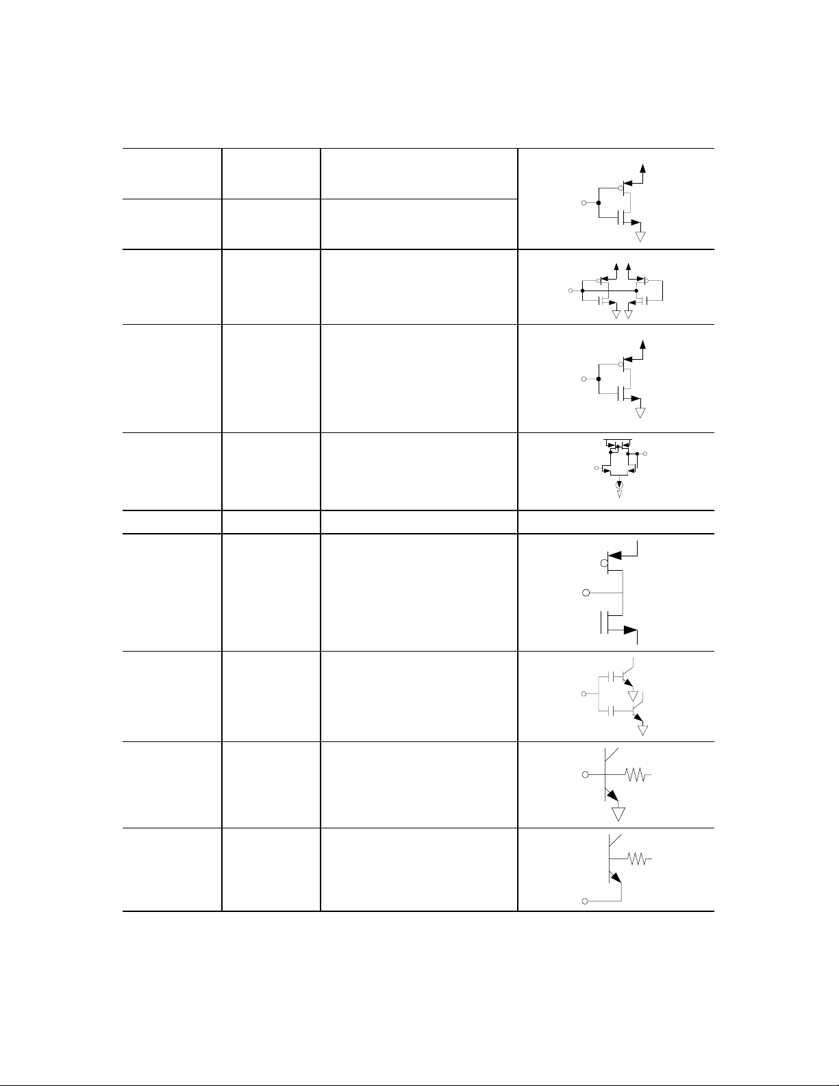
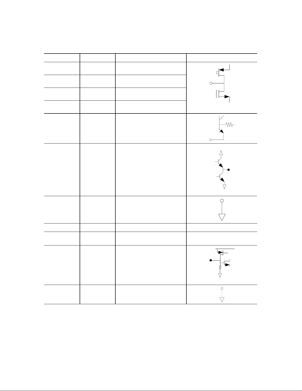
Pin # Name Description Equivalent Circuit
1 RXENA Receiver enable input
2 TXENA Transmitter enable input
3 PCO Bi-directional band select
4 VCXO_EN VCXO enable pin
Table 1. CX74063-26 Signal Descriptions (1 of 5)
5 PDETVCC Bias for the RF Detector
Vref
6 VCC1 LNA and TX charge pump supply VCC1
7 TXCPO Translational loop charge pump output
8 TXINP Translational loop feedback input
9 LNA900IN Low band LNA input for GSM850,
EGSM900
10 GNDLNA900 Low band LNA emitter ground
Vout
4 Skyworks Solutions, Inc., Proprietary and Confidential
MAY 16, 2003 [781] 376-3000 I FAX [781] 376-3100 I SALES@SKYWORKSINC.COM I WWW.SKYWORKSINC.COM 103052A
Page 5
Data Sheet I CX74063-26
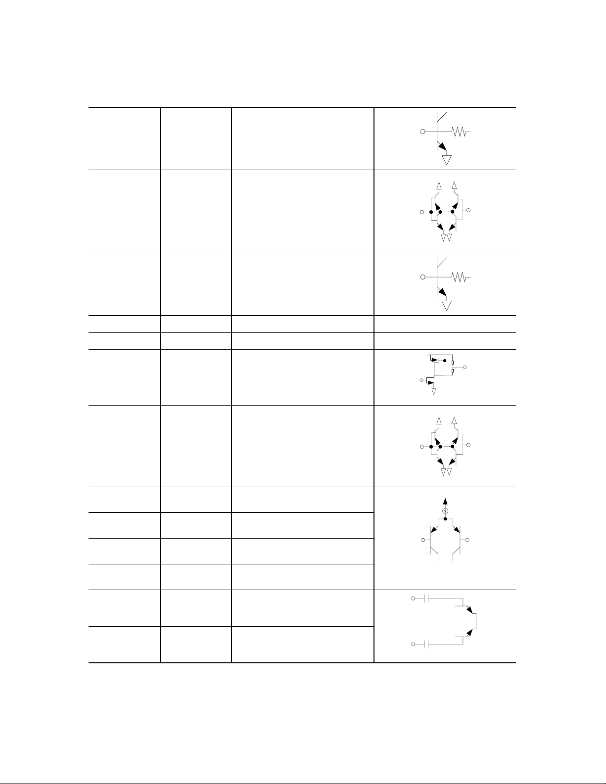
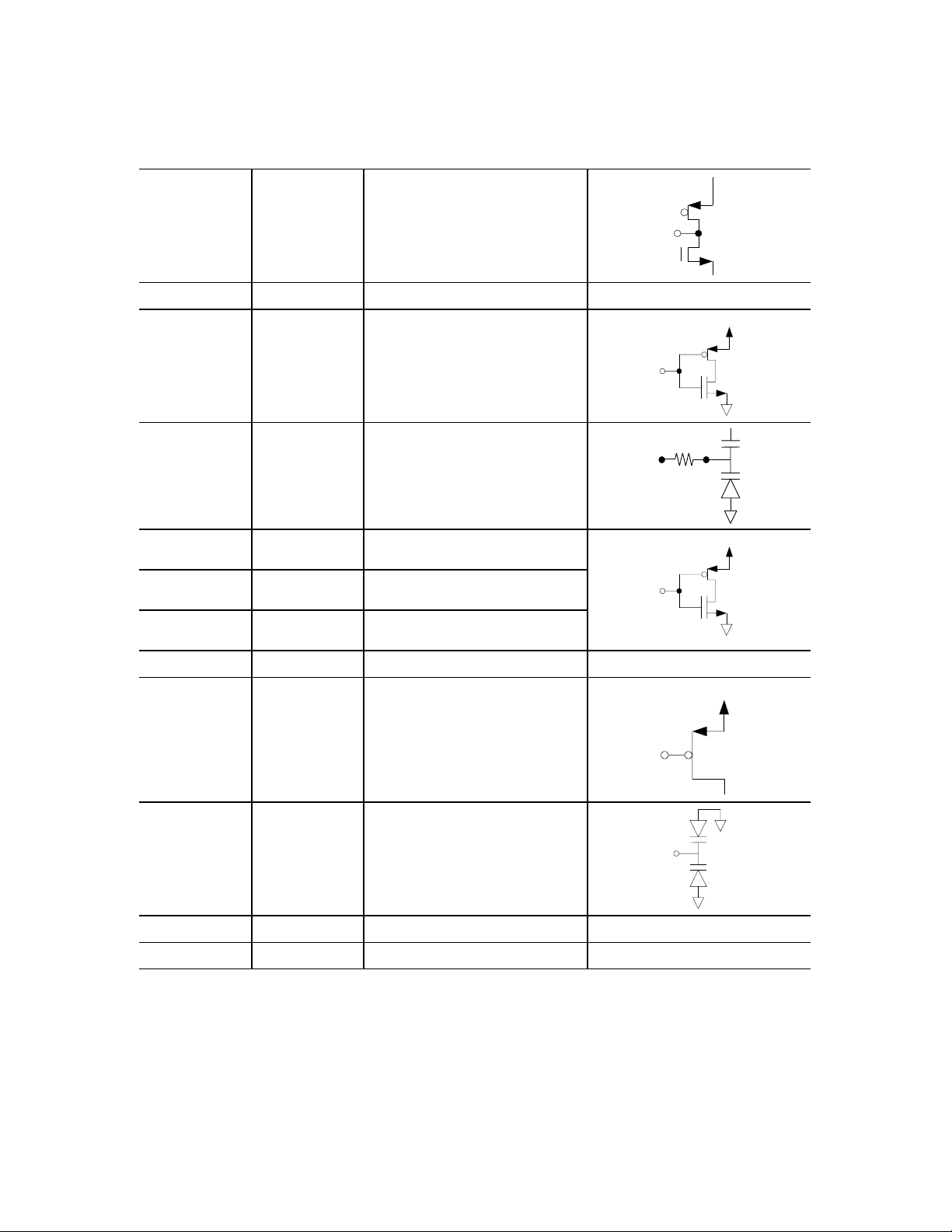
Table 1. CX74063-26 Signal Descriptions (2 of 5)
Pin # Name Description Equivalent Circuit
11 LNA1800IN DCS LNA input
12 PDET Feedback Input to power control loop
13 LNA1900IN PCS LNA input
14 NC No connect No connect
15 NC No connect No connect
16 PAVAPC PA control output
17 BBVAPC PA control Baseband input
18 TXIP TX I baseband input positive
19 TXIN TX I baseband input negative
20 TXQP TX Q baseband input positive
21 TXQN TX Q baseband input negative
22 TXFP TX IF filter output positive
Vout
23 TXFN TX IF filter output negative
Skyworks Solutions, Inc., Proprietary and Confidential 5
103052A [781] 376-3000 I FAX [781] 376-3100 I SALES@SKYWORKSINC.COM I WWW.SKYWORKSINC.COM MAY 16, 2003
Page 6
Data Sheet I CX74063-26
Pin # Name Description Equivalent Circuit
24 VCC2 RX mixer and TX loop supply VCC2
25 CAPIP Capacitor filter I positive
26 CAPIN Capacitor filter I negative
27 CAPQP Capacitor filter Q positive
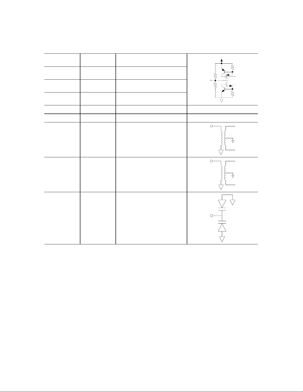
Table 1. CX74063-26 Signal Descriptions (3 of 5)
28 CAPQN Capacitor filter Q negative
29 LPFADJ LPF frequency setting resistor
30 XTALBUF Crystal oscillator buffer output
31 GNDD Synthesizer digital ground
32 VCCD Synthesizer digital supply VCCD
33 VCCF Synthesizer analog supply and crystal
oscillator supply
VCCF
34 XTAL Crystal input
35 GNDFN Synthesizer analog ground
6 Skyworks Solutions, Inc., Proprietary and Confidential
MAY 16, 2003 [781] 376-3000 I FAX [781] 376-3100 I SALES@SKYWORKSINC.COM I WWW.SKYWORKSINC.COM 103052A
Page 7
Data Sheet I CX74063-26
Table 1. CX74063-26 Signal Descriptions (4 of 5)
Pin # Name Description Equivalent Circuit
36 UHFCPO Synthesizer charge pump output
37 VCCFN_CP Synthesizer charge pump supply VCCFN_CP
38 SXENA Synthesizer enable input
39 XTALTUNE Crystal oscillator varactor control
40 DATA Serial bus data input
41 CLK Serial bus clock input
42 LE Serial bus latch enable input
43 VDDBB Digital CMOS supply VDDBB
44 UHFBYP Bypass capacitor for UHF VCO
45 UHFTUNE UHF VCO control input
46 VCCUHF UHF VCO supply VCCUHF
47 VCC3 LO chain supply VCC3
Skyworks Solutions, Inc., Proprietary and Confidential 7
103052A [781] 376-3000 I FAX [781] 376-3100 I SALES@SKYWORKSINC.COM I WWW.SKYWORKSINC.COM MAY 16, 2003
Page 8
Data Sheet I CX74063-26
Pin # Name Description Equivalent Circuit
48 RXQN Receiver output Q negative
49 RXQP Receiver output Q positive
50 RXIN Receiver output I negative
Table 1. CX74063-26 Signal Descriptions (5 of 5)
51 RXIP Receiver output I positive
52 VCC4 Baseband supply VCC4
53 VCCTXVCO Transmit VCO supply VCCTXVCO
54 TX900 Low band transmit VCO
55 TX1800/TX1900 DCS and PCS transmit VCO output
56 TXVCOTUNE Transmit VCO control input
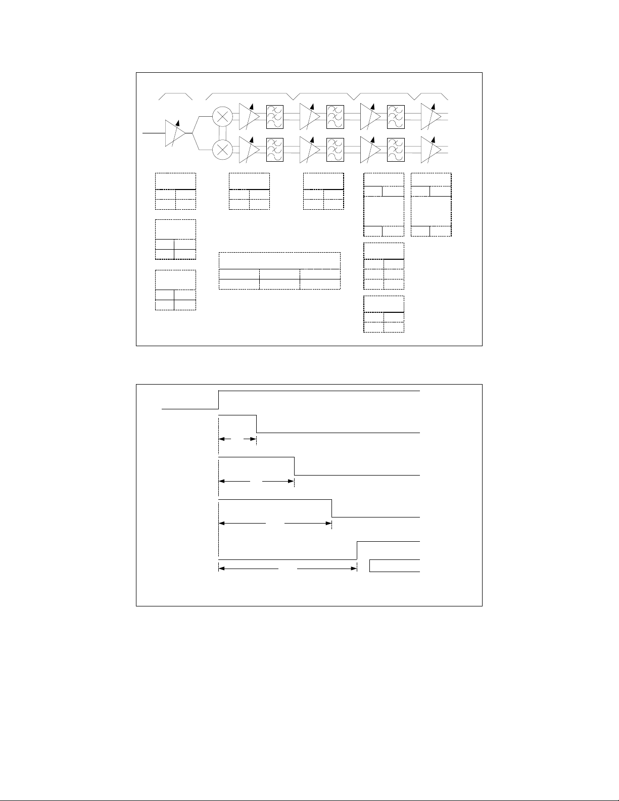
Technical Description
The CX74063-26 transceiver contains the following sections,
as shown in Figure 2.
• Receive section. Includes three integrated LNAs, a
quadrature demodulator section that performs direct down
conversion, baseband amplifier circuitry with I/Q outputs,
and three stages of DC offset correction. The receiver can
be calibrated to optimize IP2 performance.
• Synthesizer section. Includes an integrated on-chip VCO
locked by a fractional-N synthesizer loop, and a crystal
oscillator to supply the reference frequency.
• Transmit section. The TX path is a translational loop
architecture consisting of an I/Q modulator, integrated high
power VCOs, offset mixer, programmable divider, PFD, and
charge pump. The device also provides integrated gain
A 3-wire serial interface controls the transceiver and
synthesizer. The receiver gain control, as well as the division
ratios and charge pump currents in the synthesizer and
transmitter, can be programmed using 24-bit words. These
24-bit words are programmed using the 3-wire input signals
CLK, DATA, and LE. Pin 43 (VDDBB) is provided for the digital
sections to allow power supply operation compatible with
modern digital baseband devices. VDDBB is also used to
supply registers 0 through 5 to maintain programmed values.
The TXENA, RXENA, and SXENA signals separately enable the
CX74063-26 transmitter, receiver, and synthesizer sections.
TXENA and RXENA should be held low during programming.
SXENA should be held high during the programming of
register 3 (IP2 calibration). (These timing signals are detailed in
Figures 9, 10, and 11.)
controller for the PAC loop, plus the bias generator for an
external diode detector.
8 Skyworks Solutions, Inc., Proprietary and Confidential
MAY 16, 2003 [781] 376-3000 I FAX [781] 376-3100 I SALES@SKYWORKSINC.COM I WWW.SKYWORKSINC.COM 103052A
Page 9

Receive Section
LNA and Quadrature Demodulator
Three separate LNAs are integrated to address different bands
of operation. These LNAs have separate single-ended inputs,
which are externally matched to 50 Ω. The gain is switchable
between high (i.e., 15 dB typical) and low (i.e., –5 dB GSM,
–7 dB DCS, and –5 dB PCS typical) settings. The LNA outputs
feed into a quadrature demodulator that downconverts the RF
signals directly to baseband. Two external 470 pF capacitors
are required at the demodulator output to suppress the out-ofband blockers.
Baseband Section
An off-chip capacitor and three fixed poles of on-chip, low
pass filtering provide rejection of strong in- and out-of-band
interferers. In addition, a tunable, four-pole gmC filter provides
rejection of the adjacent channel blockers. Incorporated within
the fixed-pole filters are two switchable gain stages of 18 dB
and 12 dB gain steps, respectively. There is an additional
programmable gain amplifier with a gain range from 0 to + 34
dB, selectable in 2 dB steps in the four-pole tunable filter. The
final filter output feeds an amplifier with a gain range from 0 to
30 dB, selectable in 6 dB steps.
There is an additional gain stage on the four-pole tunable filter
output, the auxiliary gain stage, selectable at 0 dB or + 6 dB.
The gain control ranges are shown in Figure 3.
Recommended combinations of individual block gain settings
are shown in Table 22 for GSM900, Table 23 for DCS1800, and
Table 24 for PCS1900.
For added baseband interface flexibility, the four-pole filter, its
associated Variable Gain Amplifier (VGA), and DC offset
correction loop can be bypassed and turned off for current
savings.
In Table 2 the typical locations of all eight receiver baseband
poles are given. The final four poles are produced by the
tunable gmC filter, as set by the external resistor
(recommended value is 39.2 kΩ, 1%) placed from pin 29 to
ground.
For these tunable poles, Table 2 gives the pole location as a
function of this resistor.
Table 2. Receive Pole Locations
Data Sheet I CX74063-26
DC Offset Correction
Three DC offset correction (DCOC) loops ensure that DC
offsets, generated in the CX74063-26, do not overload the
baseband chain at any point. After compensation, the
correction voltages are held on capacitors for the duration of
the receive slot(s). Internally, on-chip timing is provided to
generate the track and hold (T_H) signals for the three
correction loops.
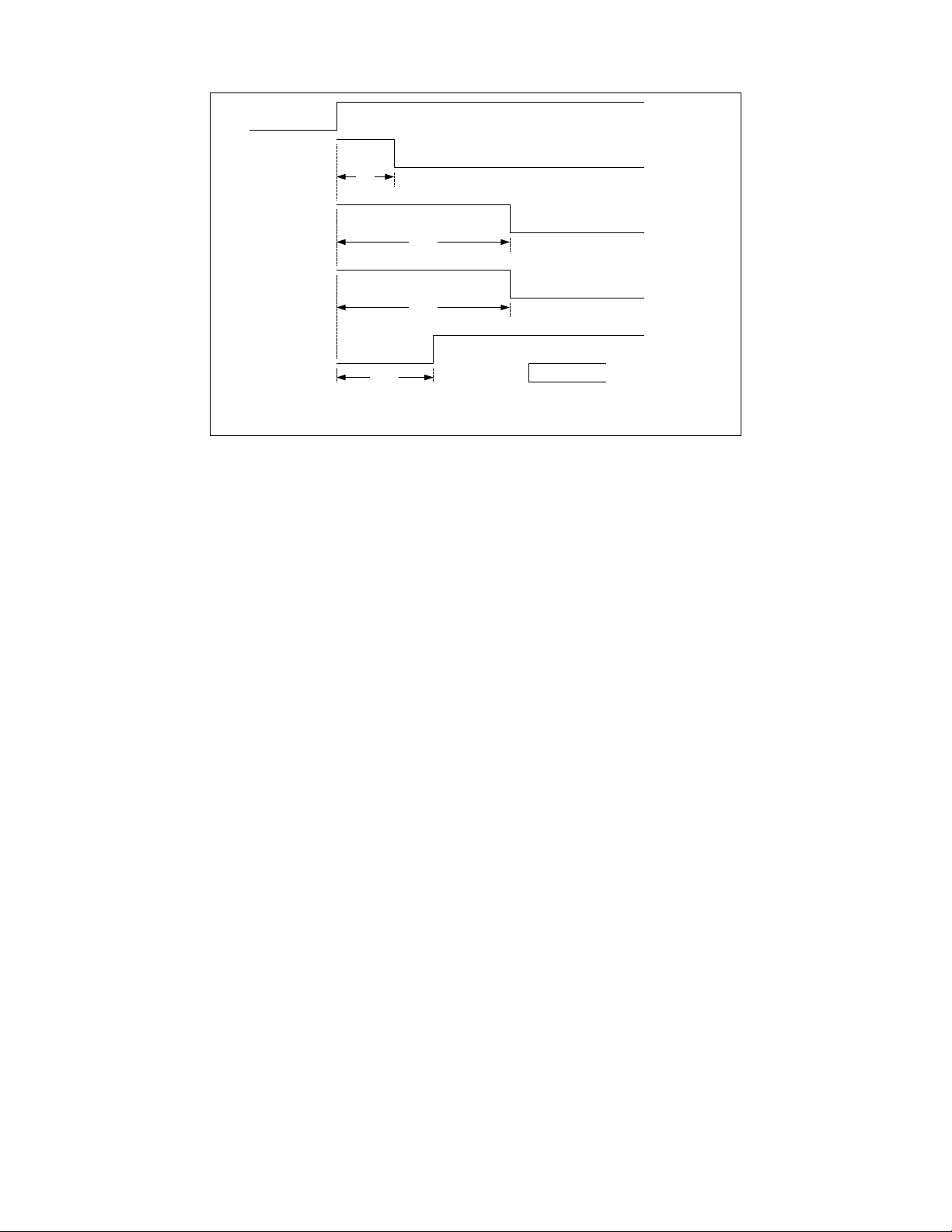
The timing diagram for the DC offset correction sequence with
reference to the receive slot is shown in Figure 4. A rising edge
on either the RXENA signal, selected via the serial interface,
places the DC compensation circuitry in the track mode.
The timing parameters for each of the three compensation
loops, t
start and the LNA being turned on, t
t_H1
, t
t_H2
, and t
, and the time between compensation
t_H3
, are defined via an
FEENA
internal state machine. The state machine is preprogrammed
with fixed default values, but may be readjusted via the serial
interface.
The timing parameters for the three compensation loops and
the LNA power-up are each independently defined, relative to
the compensation start. Therefore, they may be programmed
to occur in any order, but the sequences shown in Figure 4 and
Figure 5 are recommended. The device default timing is shown
in Figure 5, with a total time of 60 μs. Individual default timings
are given in Table 17. For user-programmed timing, the total
time may be set as short as approximately 10 μs when FREF
has a 13 MHz clock applied. However, the shortest
recommended total time is approximately 30 μs, since at the
highest gain settings, the resulting DC may degrade as
correction time is reduced.
AM Suppression and IP2 Calibration
For direct conversion GSM applications, it is imperative to have
extremely low second-order distortion. Mathematically,
second-order distortion of a constant tone generates a DCterm proportional to the square of the amplitude. A strong
interfering amplitude-modulated (AM) signal is therefore
demodulated by second-order distortion in the receiver front
end, and generates an interfering baseband signal.
Stage Typical Pole Location (rad/sec) Pole Type
–1.0 x 10⁶ Real (capacitors at pins 25-26 and 27-28 fixed at 470 pF) Mixer + RC Filter
6
Real
6
) ± j(1.35 x 10⁶)
Conjugate
Real (adjust with resistor at pin 29)
Real (adjust with resistor at pin 29)
Conjugate (adjust with resistor at pin 29)
LPF1
VGA1 + gmC filter
–1.65 x 10
(–0.91 x 10
(–0.91 x 106) x (39.2 kΩ/R)
(–0.91 x 106) x (39.2 kΩ/R)
6
[(–0.46 x 10
) ± j(1.0 x 10⁶)] x (39.2 kΩ/R)
Skyworks Solutions, Inc., Proprietary and Confidential 9
103052A [781] 376-3000 I FAX [781] 376-3100 I SALES@SKYWORKSINC.COM I WWW.SKYWORKSINC.COM MAY 16, 2003
Page 10
Data Sheet I CX74063-26
LNA Mixer + RC Filter LPF1 VGA2
GSM LNA
15 dB
High
-5 dB
Low
DCS LNA
High 15 dB
Low - 7 dB
PCS LNA
High 15 dB
Low - 5 dB
Mixer
+ RC Filter
40 dB
High
22 dB
Low
Additional Interstage Losses
GSM900
4.2 dB
DCS1800
5.0 dB
LPF1
High
Low
PCS1900
6.2 dB
10 dB
- 2 dB
VGA1 + GMC Filter
+ Aux
VGA1 +GMC
Max
30 dB
... ...
(in 6 dB steps)
Min 0 dB
VGA1 Fine
4 dB
Max
2 dB
Mid
Min 0 dB
AUX
6 dB
High
0 dB
Low
Figure 3. Gain Control Settings
VGA2
Max
30 dB
... ...
(in 6 dB steps)
Min 0 dB
101514F 5_111201
RXI+
RXI-
RXQ+
RXQ-
RXENA
DC Offset Correction Loop 1
DC Offset Correction Loop 2
DC Offset Correction Loop 3
Front End
Enable
, t
, t
Note 1. t
T_H1
T_H2
T_H3
, and t
Track mode
t
(Note 1)
Track mode
Track mode
FEENA
Hold mode (Loop
1)
T_H1
Hold mode (Loop
2)
t
T_H2
(Note 1)
t
T_H3
(Note 1)
(LNA off)
t
FEENA
(Note 1)
are programmed in Register 2.
Hold mode (Loop
3)
(LNA on)
Start of RX slot
101953A 3_012902
Figure 4. DC Offset Correction Timing (LNA Off During All of the DC Offset Correction Sequence)
10 Skyworks Solutions, Inc., Proprietary and Confidential
MAY 16, 2003 [781] 376-3000 I FAX [781] 376-3100 I SALES@SKYWORKSINC.COM I WWW.SKYWORKSINC.COM 103052A
Page 11
RXENA
Data Sheet I CX74063-26
DC Offset Correction Loop 1
DC Offset Correction Loop 2
DC Offset Correction Loop 3
Front End
Enable
Note 1. t
T_H1
, t
, t
, and t
T_H2
T_H3
Track mode
t
(Note 1)
Track mode
Track mode
FEENA
Hold mode (Loop
1)
T_H1
t
T_H2
(Note 1)
t
T_H3
(Note 1)
(LNA off)
t
FEENA
(Note 1)
are programmed in Register 2.
(LNA on)
Figure 5. DC Offset Correction Timing (LNA On During Part of the DC Offset Correction Sequence)
A commonly used measure for receiver second-order distortion
is the second-order intercept point, IP2. For example, to ensure
that the unwanted baseband signals are 9 dB below the
wanted signal required under the AM suppression test for type
approval (see 3GPP TS 51.010-1), an input IP2 of 43 dBm is
required:
The CX74063-26 receiver includes a circuit that minimizes
second-order distortion. This IP2 calibration circuit effectively
compensates any second-order distortion in the receive chain
that would otherwise generate unwanted baseband signals in
the presence of strong interfering signals. When calibrated
correctly, the CX74063-26 IP2 meets the GSM AM suppression
test requirements in all bands with good margin.
To calibrate IP2, apply a strong RF signal at the receiver input
and observe the resulting DC voltage level change at the
receiver I/Q outputs. The exact frequency and level of the
signal applied for the purpose of the calibration are not critical.
The signal should, however, be within the receive band, but at
least 6 MHz offset from the frequency to which the receiver is
tuned. The level should be high enough tocause a notable DC
shift at the I/Q outputs. A recommended value is –30 dBm at
the LNA input, which applies to all three LNAs.
A set of I/Q compensation coefficients can then be
programmed to the device to minimize the DC voltage shift
resulting from the second-order distortion. When the DC due to
the interfering signal is minimized, the IP2 performance is
optimized.
Note: SXENA, pin 38, must be held high, and a clock signal
must be present on XTAL, pin 34, during the
programming of the IP2 calibration coefficients in
register 3, see Table 18.
Hold mode (Loop
2)
Hold mode (Loop
3)
Start of RX slot
101953A 4_012902
The IP2 calibration is a one-time factory calibration that should
be done for each band and each individual device for optimum
performance. The determined coefficients must be stored in
nonvolatile memory and programmed to the CX74063-26 upon
each power-up as part of device initialization. There are onchip registers that must be programmed through register 3
with the appropriate IP2 coefficients for the band in use.
As long as a supply voltage is maintained on pin 43, VDDBB,
the IP2 coefficients for I
Lowband
, I
Highband
, Q
Lowband
, Q
Highband
,
programmed to the device remain in the registers. After the
supply voltage has been removed from VDDBB, the coefficients
must be re-programmed to the device again.
Synthesizer Section
The CX74063-26 includes a fully integrated UHF VCO with an
on-chip LC tank.
A single sigma-delta fractional-N synthesizer can phase-lock
the local oscillator used in both transmit and receive paths to a
precision frequency reference input. Fractional-N operation
offers low phase noise and fast settling times, allowing for
multiple slot applications such as GPRS. The CX74063-26
frequency stepping function with a 3 Hz resolution allows triple
band operation in both transmit and receive bands using a fully
integrated single integrated on-chip UHF VCO. The fine
synthesizer resolution allows direct compensation or
adjustment for reference frequency errors.
The fractional-N synthesizer consists of the following:
• VCO
• High frequency prescaler
• N-divider with a sigma-delta modulator
• Reference buffer and divider
• Fast phase frequency detector and charge pump
Skyworks Solutions, Inc., Proprietary and Confidential 11
103052A [781] 376-3000 I FAX [781] 376-3100 I SALES@SKYWORKSINC.COM I WWW.SKYWORKSINC.COM MAY 16, 2003
Page 12

Data Sheet I CX74063-26
The user must provide the following three parameters:
• The reference divider value, from 1 to 15
• The N-divider value, in a manner similar to an integer-N
synthesizer
• A fractional ratio
The generated frequency is given by the following equation:
FN
++
f
ref
22
2
R
where: f
N
=
f
VCO
VCO
= Generated VCO frequency
5.3
N = N-divider ratio integer part
FN = Fractional setting
R = R-divider ratio
f
REF
= Reference frequency
UHF VCO Frequency Setting
For the receiver, to tune the receive frequency, f
frequency, f
•
•
VCO, as follows:
3
f = for GSM850/900
f =
f
RXVCO
2
3
f
for DCS1800 and PCS1900
RXVCO
4
RX, set the VCO
For the transmitter VCO frequency, refer to the equations
shown in Figure 6.
Digital Frequency Centering
The CX74063-26 uses a novel technique whereby the UHF VCO
frequency range is re-centered each time the synthesizer is
programmed. This technique is called Digital Frequency
Centering (DFC). The DFC technique:
• Extends the VCO frequency coverage
• Speeds up settling time
• Ensures robust performance since the VCO is always
operated at the center of its tuning range.
Each time the synthesizer is programmed, the DFC circuit is
activated, and the VCO is centered to the programmed
frequency in less than 20 µs. After this, normal Phase Locked
Loop (PLL) operation is resumed and the fine settling of the
frequency is finalized. The DFC typically adjusts the VCO center
frequency to within a few MHz and no more than 5 MHz offset,
and presets the tuning voltage to the center of the range before
the PLL takes over. This speeds up frequency settling and
ensures that the PLL control voltage never operates close to
the rails.
Phase
Detect
D2
Ext
D1
L/C Filter
Fractional-N
PLL
UHF VCO
Ext Loop
Filter
Tx VCO
Tx I
f
VCO
90
0
Tx Q
X2
÷3
+
f
Tx
X2
where:
f
= fLO (2 D1 - D2)/D1
Tx
GSM:f
DCS/PCS: f
= (f
)/3
LO
VCO
= (2f
LO
101514D 6_071101
VCO
)/3
Figure 6. Transmitter Frequency Generation
12 Skyworks Solutions, Inc., Proprietary and Confidential
MAY 16, 2003 [781] 376-3000 I FAX [781] 376-3100 I SALES@SKYWORKSINC.COM I WWW.SKYWORKSINC.COM 103052A
Page 13

Data Sheet I CX74063-26
The DFC is an adaptive circuit that corrects for any VCO center
frequency errors caused by variations of the integrated VCO
circuit, temperature, supply voltage, aging etc. The VCO can be
centered at any frequency in the range from 1.2 GHz to
1.55 GHz. Once centered, the VCO has a minimum analog
tuning range of 30 MHz.
No calibration or data storage is needed for DFC operation. It is
activated by one of two events:
• When the synthesizer is programmed, the rising edge of the
LE signal starts the DFC cycle and,
• When changing the level of the SXENA signal from low to
high, thereby turning on the synthesizer, the rising edge of
the SXENA signal starts the DFC cycle.
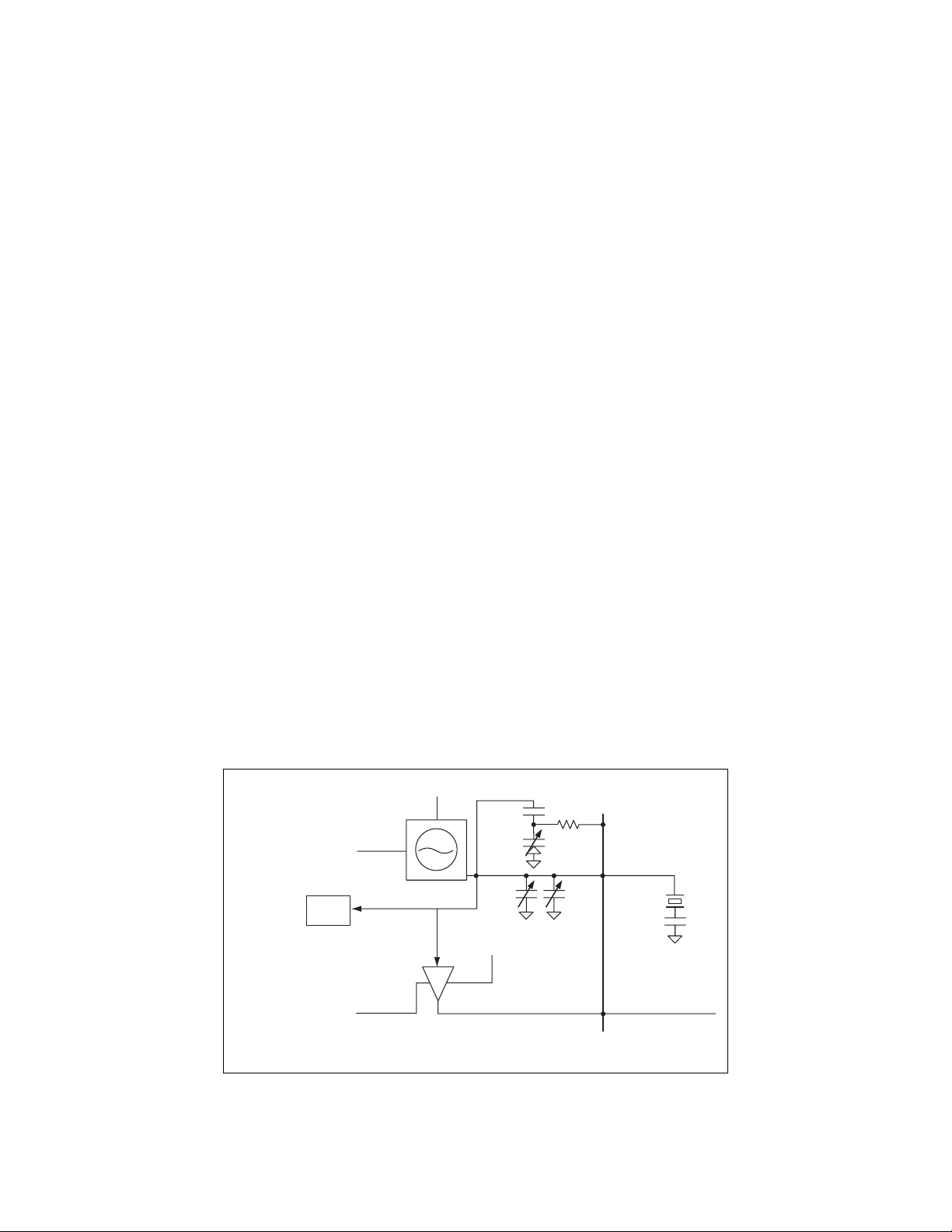
Crystal Oscillator
A crystal oscillator is designed to provide the reference
frequency for the synthesizer. As shown in Figure 7, the
oscillator uses an external crystal to generate an accurate
oscillation frequency. The reference frequency can be changed
through coarse tuning with an integrated capacitor array or fine
tuning with the integrated varactor diode. The coarse tuning is
done by switching in and out (using a digital word programmed
via the serial interface) the capacitor network (CAP_A and
CAP_B) located at the input of the integrated buffer. The fine
tuning is done by providing a tuning voltage to the integrated
varactor diode. Table 20 describes the control bits.
An output buffer is provided to drive the baseband circuitry
(XTALBUF, pin 30). The VCXO and buffer circuitry are powered
from pin 33 (VCCF). When VCCF is ramped to a voltage greater
than 2.6 V, the output buffer powers on. The oscillator core
powers up when pin 4 (VCXO_EN) is set to logic 1. If pin 4 is
tied permanently to logic 1, the R6 VCXO Control Register is set
to a defined state by a power-on reset. Pin 4 should be held
low if an external reference oscillator is used. The buffer may
be disabled by programming bit 3 in the SX1 Control Register
(see Table 13) to logic 0.
Transmit Section
To minimize the post-PA filtering requirements and any
additional post-PA losses, the transmit path consists of a
vector modulator within a frequency translation loop. The
translation loop consists of the following:
• Phase Frequency Detector (PFD) and charge pump
• Mixer with an operating range of 800 MHz to 2 GHz
• An in-loop modulator
• Two programmable dividers
• Two transmit VCOs
Translational Loop
The translational loop takes baseband analog I/Q signals and
modulates them with the mixed product of transmitter output
and LO signal, as shown in Figure 6. The unmodulated result is
compared with a divided down LO at the PFD and the
difference is used to control the transmit VCO. The on-chip
Low Pass Filter (LPF) following the mixer attenuates the
unwanted sidebands as well as harmonics.
Transmit VCOs
Two on-chip transmit VCOs are designed to meet GSM850,
EGSM900, DCS1800, and PCS1900 requirements. The
transmit VCOs use the same DFC technique as described in the
Synthesizer section to lock the translational loop. The rising
edge on TXENA initializes the transmit DFC.
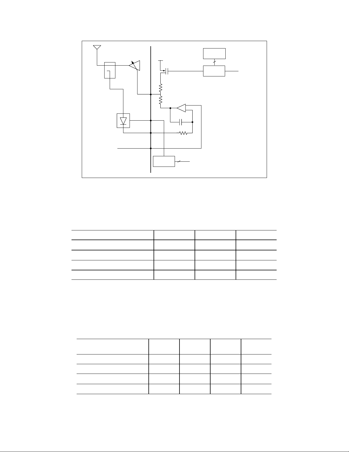
Power Amplifier Gain Controller
The device contains an error amplifier/integrator to provide
transmit burst control for an external power amplifier (PA). As
shown in Figure 8, when the device is connected to a PA, an
RF detector, and a coupler, a loop is formed that controls the
transmit power in a multi-band wireless application. The error
amplifier amplifies and integrates the voltage difference
between the RF detector output (PDET) and the power control
input (BBVAPC). The output of the integrator is fed to an
internal gain shaper that drives the gain control input (PAVAPC)
of the external RF PA. The device. provides a bandgap voltage
(PDETVCC) which can be used as the supply voltage for the
external peak detector and can source up to 200 µA.
The PA pre-bias is activated after a programmable delay and
time-referenced from the rising edge of TXENA. The time delay
is set using the serial interface. See Table 19 for details.
Digital Interface
The transceiver and synthesizer are controlled by a single
three-wire serial interface. The transmitter, receiver, and
synthesizer are each enabled through external inputs
according to typical timing requirements as shown in Figures
10 and 11.
Band selection for the CX74063-26 is through the three-wire
serial interface. The PCO signal (pin 3) provides a band
selection control output. DC offset calibration and front-end
activation timing can also be controlled by an on-chip signal
sequencer, precluding the need for separate control signals. All
the logic and the three-wire interface inputs are referenced to
the PCO signal (pin 3).
The RX/TX Control Register is used to program the transceiver
and to preset other test word states by setting bit 22 as a
logic 1. If any test words are to be altered from their preset
states, bit 22 must be sent to the RX/TX Control Register again
as a logic 0. Typically, this is done only on power-up since the
device has a zero-power standby mode that retains
programmed test memory.
There are seven additional registers used to program various
functions of the CX74063-26. The SX1 Control Register is used
to program the fractional-N synthesizer and the SX2
Fractional-N Modulo Register is used to program the modulus.
Three auxiliary registers are used to program the transceiver
besides the RX/TX Control Register, and two 24-bit registers
are used to program the synthesizer:
• SX1 Control
• SX2 Fractional-N Modulo
• RX/TX Control
• R0 Auxiliary Control
Skyworks Solutions, Inc., Proprietary and Confidential 13
103052A [781] 376-3000 I FAX [781] 376-3100 I SALES@SKYWORKSINC.COM I WWW.SKYWORKSINC.COM MAY 16, 2003
Page 14
Data Sheet I CX74063-26
• R2 DC Offset Timing
• R3 IP2 Calibration
• R6 VCXO Control
• R7 VCXO Control
SX1 Control Register. This register is used to program the
fractional-N synthesizer, and set the values of the integral-N
divider and the input-R divider. The polarity of the
Phase/Frequency Detector (PFD) may also be defined by this
register. Refer to Table 13.
SX2 Fractional-N Modulo Register. This register is used to
program the 24-bit modulo of the fractional-N synthesizer. The
data is a 22-bit binary coded decimal word that allows the PLL
to lock to precise frequencies. Refer to Table 14.
RX/TX Control Register. This register is used to control divide
ratios and charge pump currents in the transmitter, and to
control gain in the receiver along with the band select function.
Refer to Table 15.
R0 Auxiliary Control Register. This register is used to bypass
the DC offset correction loops and the baseband filters. It also
enables and disables the two on-chip transmit VCOs and
defines the directionality of the LO port, which allows an
external VCO or LO reference to be used or enables the internal
VCO to be monitored. Refer to Table 16.
R2 DC Offset Timing Register. This register sets the timing of
the tracking of the three DC offset cancellation loops and the
time at which the front end turns on relative to the RXENA
signal (pin 1). It allows the front-end to be enabled using the
internal timer. Refer to Table 17.
R3 IP2 Calibration Register. This register is used to perform
nd
2
order Intercept Point (IP2) calibration by manually adjusting
calibration coefficients. A total of four words need to be set:
IP2 coefficients for I-high band, I-low band, Q-high band, and
Q-low band. Refer to Table 18.
The IP2 coefficient is eight bits long (including polarity) and is
intended to be a factory calibration. An algorithm using a test
tone needs to be used to determine the coefficient for each
individual part.
R4 PAC Timing Control Register. This register is used to set
timing for the PAC pedestal. See Table 19.
R6 and R7 VCXO Control Registers. These registers are used
to control the tuning range and oscillation frequency of the
VCXO. See Tables 20 and 21, respectively.
Electrical and Mechanical Specifications
The absolute maximum ratings of the CX74063-26 are
provided in Table 3. The recommended operating conditions
are specified in Table 4. Electrical specifications are provided
in Tables 5 through 11. Tables 12 through 21, and Figures 9
through 11 provide the serial interface programming states,
functions, and timing curves. Receiver data is shown in Tables
22 through 33 and illustrated in Figures 12 through 20.
Transmit data is illustrated in Figures 21 through 26.
A typical application circuit using the CX74063-26 is shown in
Figure 27. The 56-pin RFLGA package dimensions are
provided in Figure 28 and the tape and reel dimensions are
shown in Figure 29.
Electrostatic Discharge
The CX74063-26 contains Class 1 devices. The following
Electrostatic Discharge (ESD) precautions are recommended:
• Protective outer garments
• Handle device in ESD safeguarded work area
• Transport device in ESD shielded containers
• Monitor and test all ESD protection equipment
• Treat the CX74063-26 as extremely sensitive to ESD
VCCF (Pin 33)
VCXO_EN (Pin 4)
[SX Register 1
(bit 3)]
PLL
BUF_EN
Baseband
Buffer
100 kΩ
CAP_B
VCCF (Pin 33)
XTALTUNE (Pin 39)
XTAL (Pin 34)
CAP_A
XTAL_BUF (Pin 30)
to baseband
C1337
Figure 7. VCXO Block Diagram
14 Skyworks Solutions, Inc., Proprietary and Confidential
MAY 16, 2003 [781] 376-3000 I FAX [781] 376-3100 I SALES@SKYWORKSINC.COM I WWW.SKYWORKSINC.COM 103052A
Page 15
Data Sheet I CX74063-26
Coupler
Power Detector
from baseband
PA
PAVAPC
(pin 16)
PDETVCC
(pin 5)
PDET
(pin 12)
BBVAPC (pin 17)
VCC2
Bias
Generator
5 pF
10 kΩ
1
+
–
Register 4
8
PAC Delay
Timer
Rx/Tx Control Register
(bit 21), PDETVCC
0 = 0.5 V
1 = 1.0 V
TXENA (pin 2)
C1338a
Figure 8. PA Controller Block Diagram
Table 3. CX74063-26 Absolute Maximum Ratings
Parameter Minimum Maximum Units
Supply voltage (VCC) –0.3 +3.6 V
Ambient operating temperature range –40 +95
Storage temperature range –50 +125
°C
°C
Input voltage range GND VCC V
Maximum power dissipation 600 mW
Note: Stresses above these absolute maximum ratings may cause permanent damage. These are
stress ratings only and functional operation at these conditions is not implied. Exposure to
maximum rating conditions for extended periods may reduce device reliability.
Table 4. CX74063-26 Recommended Operating Conditions
Parameter Minimum Typical Maximum Units
LNA input level (pins 9, 11, 13)
RXEN = Off
Power supply 2.6 2.8 3.3 V
Digital power supply, VDDBB 1.8 3.3 V
Operating junction temperature –40 +110
Operating ambient temperature –30 +85
10 dBm
°C
°C
Skyworks Solutions, Inc., Proprietary and Confidential 15
103052A [781] 376-3000 I FAX [781] 376-3100 I SALES@SKYWORKSINC.COM I WWW.SKYWORKSINC.COM MAY 16, 2003
Page 16
Data Sheet I CX74063-26
Parameter Symbol Test Condition Min Typical Max Units
Total supply current:
Rx section, EGSM/GSM850
Tx section, EGSM/GSM850 (includes TX VCO)
Synthesizer section, EGSM/GSM850
(includes UHF VCO)
Rx section, DCS/PCS
Tx section, DCS/PCS (includes TX VCO)
Synthesizer section, DCS/PCS (includes UHF
VCO)
Sleep mode
Table 5. Power Consumption Specifications
(TA = 25° C, VCC = 2.8 V unless otherwise noted)
ICC
RXENA=H; SXENA=L
TXENA=H; SXENA=L
SXENA=H
RXENA=H; SXENA=L
TXENA=H; SXENA=L
SXENA=H
@ VCC = 3.3 V
RXENA=L; TXENA=L;
SXENA=L
41
121
39
49
126
39
20
48
137
46
58
143
46
100
mA
mA
mA
mA
mA
mA
µA
16 Skyworks Solutions, Inc., Proprietary and Confidential
MAY 16, 2003 [781] 376-3000 I FAX [781] 376-3100 I SALES@SKYWORKSINC.COM I WWW.SKYWORKSINC.COM 103052A
Page 17

Table 6. CX74063-26 Electrical Specifications – EGSM/GSM850 Receiver (1 of 3)
(TA = 25° C, VCC = 2.8 V unless otherwise noted)
Data Sheet I CX74063-26
Parameter Symbol Test Condition
Min Typical Max Units
(Note 1)
Input impedance. See Figure 12 for unmatched
input impedance.
Input operating frequency Band 1 869 960 MHz
Receiver maximum voltage gain GRXMAX Highest gain mode 120 126 dB
Receiver minimum voltage gain GRXMIN Lowest gain mode 11 17 dB
Receiver gain temperature variation GTEMPVAR
Gain step
Gain step accuracy GSTEP Over range
Gain variation versus frequency GFREQ Over 869-894 MHz
Noise Figure NFGAIN1 G = 15/40/10/12/0/18 3.2 3.9 dB
Noise Figure (temperature) NFTEMP
Noise Figure degradation in presence of blocker NFBLOC With –26 dBm input
ZIN With external match 50
4.5 dB
∆A
T
A = –30 °C to +85 °C
V
2 dB
–0.75 +0.75 dB
recommended in
Table 25
2 2 dB
Over 925-960 MHz
T
A = +75 °C
T
A= +85 °C
5.0
G = 15/40/10/12/0/18
2
blocker @ 3 MHz
offset (ideal LO)
Internal LO
4
G = 15/40/10/12/0/18
Ω
dB
dB
5.2
dB
dB
dB
Input 2nd order intercept point IIP2 Referred to LNA input
50 65 dBm
calibrated and
measured at middle of
EGSM or GSM850
band.
DC shift in presence of blocker AM Supp With –34 dBm
17 mV
@ 6 MHz offset
G = 15/40/10/12/0/18
LO Re-radiation @ LNA input LOREV @ wanted frequency –110 –100 dBm
Selectivity @ 3 MHz offset
@ 1.6 MHz offset
@ 600 kHz offset
@ 400 kHz offset
@ 200 kHz offset
T
A = –30 °C to +85 °C
143
128
61
37
9
137
68
44
13
dB
dB
dB
dB
dB
Skyworks Solutions, Inc., Proprietary and Confidential 17
103052A [781] 376-3000 I FAX [781] 376-3100 I SALES@SKYWORKSINC.COM I WWW.SKYWORKSINC.COM MAY 16, 2003
Page 18
Data Sheet I CX74063-26
Table 6. CX74063-26 Electrical Specifications – EGSM/GSM850 Receiver (2 of 3)
(TA = 25° C, VCC = 2.8 V unless otherwise noted)
Parameter Symbol Test Condition
(Note 1)
I/Q amplitude imbalance
I/Q phase imbalance
Input 1 dB compression point IP1dB F = 200 kHz,
3rd order intercept point @ +25 °C
3rd order intercept point @ –20 °C
IIP3 F = 3.0 MHz
IIP3 F = 3.0 MHz
Output offset voltage With DC offset
T
A = –30 °C to +85 °C
T
A = –30 °C to +85 °C
G = 15/40/-2/8/0/18
F = 400 kHz,
G = 15/40/-2/8/0/18
F = 600 kHz,
G = 15/40/10/12/0/18
F = 1.6 MHz,
G = 15/40/10/12/0/18
F = 3.0 MHz,
G = 15/40/10/12/0/18
G = 15/40/10/12/0/18
G = 15/40/10/12/0/18
corrected while LNA is
off
A = +85°C
T
With DC offset
corrected while LNA is
on
G=15/40/10/12/0/18
A = +85 °C
T
Min Typical Max Units
1 dB
–3 +3 degrees
–65
–45
–35
–32
–25
–15 –12 dBm
–15 –12 dBm
200
–60
–40
–30
–28
–22
dBm
dBm
dBm
dBm
dBm
mV
220
20
25
mV
mV
mV
(60 µs total DC
correction time)
Offset drift (long term) DCDRFT1 G = 15/40/10/12/0/18
100 mV
50 ms after correction
Offset drift (short term) DCDRFT2 G = 15/40/10/12/0/18
10 mV
577 µs after
correction
Baseband Tunable Active Filter
3 dB corner frequency (tunable) FC 80 100 kHz
Corner frequency variation dFC
39.2 kΩ at pin 29
–11 +11 %
470 pF at pins 25-26
and 27-28
18 Skyworks Solutions, Inc., Proprietary and Confidential
MAY 16, 2003 [781] 376-3000 I FAX [781] 376-3100 I SALES@SKYWORKSINC.COM I WWW.SKYWORKSINC.COM 103052A
Page 19
Table 6. CX74063-26 Electrical Specifications – EGSM/GSM850 Receiver (3 of 3)
(TA = 25° C, VCC = 2.8 V unless otherwise noted)
Data Sheet I CX74063-26
Parameter Symbol Test Condition
Min Typical Max Units
(Note 1)
Receiver Output Stage
Differential output amplitude
(pk/pk differential)
Output common mode voltage
VGA2 = 30 dB
VGA2
= 0 dB
T
A = –30 °C to +85 °C
3.7
0.3
VCC/2 –
0.1
V
V
VCC/2 VCC/2 +
V
0.1
Maximum current drive IOUT 0.5 mA
Output resistance ROUT 160 200 240
Ω
Output capacitance COUT 1 pF
Note 1: Gain codes refer to LNA/Mixer/LPF1/VGA1/AUX/VGA2 gains in dB.
Table 7. CX74063-26 Electrical Specifications – DCS1800 Receiver (1 of 3)
(TA = 25° C, VCC = 2.8 V unless otherwise noted)
Parameter Symbol Test Condition
Min Typical Max Units
(Note 1)
Input impedance See Figure 13 for unmatched
input impedance.
ZIN With external match 50
Ω
Input operating frequency Band 2 DCS Rx band 1805 1880 MHz
Receiver maximum voltage gain GRXMAX Highest gain mode 117 123 dB
Receiver minimum voltage gain GRXMIN Lowest gain mode 9 15 dB
Gain step
∆A
V
Receiver gain temperature variation GTEMPVAR
Gain step accuracy GSTEP Over range
2 dB
T
A = –30 °C to +85 °C
4.5 dB
–0.75 +0.75 dB
recommended in
Table 26
Gain variation versus frequency GFREQ Over band 2 2 dB
Noise Figure NFGAIN1 G = 15/40/10/12/0/18 3.6 4.3 dB
Noise Figure (temperature) NFTEMP
T
A = +75 °C
A = +85 °C
T
Noise Figure degradation in presence of blocker NFBLOC With –30 dBm input
blocker @ 3 MHz
offset (ideal LO)
Internal LO
5.4
5.6
2
dB
4
G = 15/40/10/12/0/18
dB
dB
Skyworks Solutions, Inc., Proprietary and Confidential 19
103052A [781] 376-3000 I FAX [781] 376-3100 I SALES@SKYWORKSINC.COM I WWW.SKYWORKSINC.COM MAY 16, 2003
Page 20

Data Sheet I CX74063-26
Table 7. CX74063-26 Electrical Specifications – DCS1800 Receiver (2 of 3)
(TA = 25° C, VCC = 2.8 V unless otherwise noted)
Parameter Symbol Test Condition
Min Typical Max Units
(Note 1)
Input 2nd order intercept point IIP2 Referred to LNA input
calibrated and
measured at middle of
DCS1800 band.
DC shift in presence of blocker AM Supp With –33 dBm
@ 6 MHz offset
G = 15/40/10/12/0/18
LO re-radiation @ LNA input LOREV @ wanted frequency –110 –100 dBm
Selectivity @ 3 MHz offset
@ 1.6 MHz offset
@ 600 kHz offset
@ 400 kHz offset
@ 200 kHz offset
T
A = –30 °C to +85 °C
I/Q amplitude imbalance
I/Q phase imbalance
T
A = –30 °C to +85 °C
T
A = –30 °C to +85 °C
Input 1 dB compression point IP1dB F = 200 kHz,
G = 15/40/-2/8/0/18
F = 400 kHz,
G = 15/40/-2/8/0/18
F = 600 kHz,
G = 15/40/10/12/0/18
F = 1.6 MHz,
G = 15/40/10/12/0/18
F = 3.0 MHz,
G = 15/40/10/12/0/18
50 65 dBm
17 mV
143
128
61
37
9
137
68
41
13
dB
dB
dB
dB
dB
1 dB
–3 +3 degrees
–65
–45
–35
–32
–25
–60
–40
–30
–28
–22
dBm
dBm
dBm
dBm
dBm
3rd order intercept point @ +25 °C
IIP3 F = 3.0 MHz
–15 –12 dBm
G = 15/40/10/12/0/18
3rd order intercept point @ –20 °C
IIP3 F = 3.0 MHz
–15 –12 dBm
G = 15/40/10/12/0/18
20 Skyworks Solutions, Inc., Proprietary and Confidential
MAY 16, 2003 [781] 376-3000 I FAX [781] 376-3100 I SALES@SKYWORKSINC.COM I WWW.SKYWORKSINC.COM 103052A
Page 21
Table 7. CX74063-26 Electrical Specifications – DCS1800 Receiver (3 of 3)
(TA = 25° C, VCC = 2.8 V unless otherwise noted)
Data Sheet I CX74063-26
Parameter Symbol Test Condition
Min Typical Max Units
(Note 1)
Output offset voltage With DC offset
corrected while LNA is
off
A = + 85°C
T
With DC offset
corrected while LNA is
on
G=15/40/10/12/0/18
A = + 85 °C
T
(60 µs total DC
correction time)
Offset drift (long term) DCDRFT1 G=15/40/10/12/0/18
50 ms after correction
Offset drift (short term) DCDRFT2 G=15/40/10/12/0/18
577 µs after
correction
Baseband Tunable Active Filter
3 dB corner frequency (tunable) FC 80 100 kHz
Corner frequency variation dFC
39.2 kΩ at pin 29
470 pF at pins 25-26
and 27-28
Receiver Output Stage
200
220
20
25
mV
mV
mV
mV
100 mV
10 mV
–11 +11 %
Differential output amplitude (pk/pk differential) VGA2 = 30 dB
VGA2
= 0 dB
3.7
0.3
Output common mode voltage VCC/2 –
0.1
V
VCC/2 VCC/2 +
0.1
V
V
Maximum current drive IOUT 0.5 mA
Output Resistance ROUT 160 200 240
Ω
Output Capacitance COUT 1 pF
Note 1: Gain codes refer to LNA/Mixer/LPF1/VGA1/AUX/VGA2 gains in dB.
Skyworks Solutions, Inc., Proprietary and Confidential 21
103052A [781] 376-3000 I FAX [781] 376-3100 I SALES@SKYWORKSINC.COM I WWW.SKYWORKSINC.COM MAY 16, 2003
Page 22
Data Sheet I CX74063-26
Table 8. CX74063-26 Electrical Specifications – PCS1900 Receiver (1 of 3)
(TA =2 5° C, VCC = 2.8 V unless otherwise noted)
Parameter Symbol Test Condition
Min Typical Max Units
(Note 1)
Input impedance. See Figure 14 for unmatched
input impedance.
Input operating frequency Band 3 PCS Rx band 1930 1990 MHz
Receiver maximum voltage gain GRXMAX Highest gain mode 117 123 dB
Receiver minimum voltage gain GRXMIN Lowest gain mode 7 13 dB
Receiver gain temperature variation GTEMPVAR
Gain step
Gain step accuracy GSTEP Over range
Gain variation versus frequency GFREQ Over band 3 2 dB
Noise Figure NFGAIN1 G = 15/40/10/14/0/18 4.2 4.9 dB
Noise Figure (temperature) NFTEMP
Noise Figure degradation in presence of blocker NFBLOC With –30 dBm input
ZIN With external match 50
4.5 dB
∆A
T
A = –30 °C to +85 °C
V
2 dB
–0.75 +0.75 dB
recommended in
Table 27
T
A = +75 °C
A = +85 °C
T
6.0
2
blocker @ 3MHz
offset (ideal LO)
Internal LO
4
G = 15/40/10/14/0/18
Ω
dB
6.2
dB
dB
Input 2nd order intercept point IIP2 Referred to LNA input
50 65 dBm
calibrated and
measured at middle of
PCS1900 band
DC shift in presence of blocker AM Supp With –33 dBm
17 mV
@ 6 MHz offset
G = 15/40/10/14/0/18
LO Re-radiation @ LNA input LOREV @ wanted frequency –110 –100 dBm
Selectivity @ 3 MHz offset
@ 1.6 MHz offset
@ 600 kHz offset
@ 400 kHz offset
@ 200 kHz offset
T
A = –30 °C to +85 °C
I/Q amplitude imbalance
I/Q phase imbalance
T
A = –30 °C to +85 °C
T
A = –30 °C to +85 °C
143
128
61
37
9
137
68
41
13
1 dB
–3 +3 degrees
dB
dB
dB
dB
dB
22 Skyworks Solutions, Inc., Proprietary and Confidential
MAY 16, 2003 [781] 376-3000 I FAX [781] 376-3100 I SALES@SKYWORKSINC.COM I WWW.SKYWORKSINC.COM 103052A
Page 23
Table 8. CX74063-26 Electrical Specifications – PCS1900 Receiver (2 of 3)
(TA =2 5° C, VCC = 2.8 V unless otherwise noted)
Data Sheet I CX74063-26
Parameter Symbol Test Condition
(Note 1)
Input 1 dB compression point IP1dB F = 200 kHz,
G = 15/40/-2/8/0/18
F = 400 kHz,
G = 15/40/-2/8/0/18
F = 600 kHz,
G = 15/40/10/14/0/18
F = 1.6 MHz,
G = 15/40/10/14/0/18
F = 3.0 MHz,
G = 15/40/10/14/0/18
3rd order intercept point @ +25 °C
3rd order intercept point @ –20 °C
Output offset voltage With DC offset
IIP3 F = 3.0 MHz
G = 15/40/10/14/0/18
IIP3 F = 3.0 MHz
G = 15/40/10/14/0/18
corrected while LNA is
off
A = + 85°C
T
With DC offset
corrected while LNA is
on
G = 15/40/10/12/0/18
A = + 85 °C
T
Min Typical Max Units
–65
–45
–35
–32
–25
–15 –12 dBm
–15 –12 dBm
200
–60
–40
–30
–28
–22
dBm
dBm
dBm
dBm
dBm
mV
220
20
25
mV
mV
mV
(60 µs total DC
correction time)
Offset drift (long term) DCDRFT1 50 ms after correction
100 mV
G = 15/40/10/14/0/18
Offset drift (short term) DCDRFT2
577 µs after
10 mV
correction
G = 15/40/10/14/0/18
Baseband Tunable Active Filter
3 dB corner frequency (tunable) FC 80 100 kHz
Corner frequency variation dFC
39.2 kΩ at pin 29
–11 +11 %
470 pF at pins 25-26
and 27-28
Skyworks Solutions, Inc., Proprietary and Confidential 23
103052A [781] 376-3000 I FAX [781] 376-3100 I SALES@SKYWORKSINC.COM I WWW.SKYWORKSINC.COM MAY 16, 2003
Page 24
Data Sheet I CX74063-26
Table 8. CX74063-26 Electrical Specifications – PCS1900 Receiver (3 of 3)
(TA =2 5° C, VCC = 2.8 V unless otherwise noted)
Parameter Symbol Test Condition
Min Typical Max Units
(Note 1)
Receiver Output Stage
Differential output amplitude (pk/pk differential) VGA2 = 30 dB
VGA2
= 0 dB
3.7
0.3
Output common mode voltage VCC/2 –
0.1
V
VCC/2 VCC/2 +
0.1
V
V
Maximum current drive IOUT 0.5 mA
Output resistance ROUT 160 200 240
Ω
Output capacitance COUT 1 pF
Note 1: Gain codes refer to LNA/Mixer/LPF1/VGA1/AUX/VGA2 gains in dB.
Table 9. CX74063-26 Electrical Specifications – Transmitter (1 of 4)
(TA = 25° C, VCC = 2.8 V unless otherwise noted)
Parameter Symbol Test Condition Min Typical Max Units
I/Q Modulator
Differential input impedance ZIN 16 20 24
Input signal level Differential 0.8 1 1.2 Vp-p
Input common mode voltage range VCM 0.85 1.35 VCC –
1.3
Input frequency 3 dB bandwidth 3 MHz
Input common mode rejection ratio fIN = 100 kHz
f
IN = 1 MHz
65
45
75
55
dB
Output operating frequency FOUT 70 130 MHz
Output impedance ZOUT Per side 170 200 230
Output voltage VOUT –33 dBV
Output noise power NO @ 10 MHz offset
@ 1.8 MHz offset
–132
–130
–128
–126
LO suppression 30 35 dBc
Sideband suppression 30 35 dBc
Translational Loop
kΩ
V
Ω
dBc/Hz
dBc/Hz
Spurious Modulation 2nd order
Modulation 3rd order
–70
–60
–40
–55
dBc
dBc
Transmit frequency (input from VCO) FTX 800 2000 MHz
IF frequency
Transmit input power PIN
FIF
70 130 MHz
With external 50 Ω
–20 –15 –10 dBm
termination
24 Skyworks Solutions, Inc., Proprietary and Confidential
MAY 16, 2003 [781] 376-3000 I FAX [781] 376-3100 I SALES@SKYWORKSINC.COM I WWW.SKYWORKSINC.COM 103052A
Page 25
Data Sheet I CX74063-26
Table 9. CX74063-26 Electrical Specifications – Transmitter (2 of 4)
(TA = 25° C, VCC = 2.8 V unless otherwise noted)
Parameter Symbol Test Condition Min Typical Max Units
Translational Loop (continued)
Transmit input impedance ZIN 300//
0.3
Transmitter output phase noise (includes TX VCO
and LO PLL)
NO @ 400 kHz offset
@ 1.8 MHz offset
@ 10 MHz offset
EGSM/GSM850
@ 20 MHz offset
EGSM/GSM850
@ 20 MHz offset
–120
–130
–152
–164
–156
–118
–124
–150
–162
–154
Ω//
pF
dBc/Hz
dBc/Hz
dBc/Hz
dBc/Hz
dBc/Hz
DCS/PCS
Tx phase error TxPHERR rms (employs
2.0 degrees
reference frequency
source, and loop
filters as shown in the
reference design)
Charge pump output current: high impedance
source/sink
IOUT RX/TX control register
bits
S15 S14
CP = 0 0
CP = 0 1
CP = 1 0
CP = 1 1
±0.5
±0.75
±1.0
±1.25
mA
mA
mA
mA
Charge pump current variation 0.3 ≤ VCPO ≤ VCC – 0.5 20 %
Charge pump current variation over temperature 0.3 ≤ VCPO ≤ VCC – 0.5
10 %
TA = –30 °C to +85 °C
D1 divide ratio range 9 12
D2 divide ratio 1 2
Tx mixer
LO leakage
TXMIX
LEAKAGE
Tx mixer
50 Ω terminated
–60 dBm
Low Band Translation Loop VCO
Center frequency fC
T
A = –30 °C to +85 °C
800 930 MHz
Digital frequency centering resolution eDFC 2.5 MHz
Digital frequency centering time tDFC From rising edge of
12 20
µs
TXENA (13 MHz clock
frequency)
Digital frequency centering voltage VDFC (Control voltage at end
of DFC and start of
VCC/2 –
0.2
VCC/2 VCC/2 +
0.2
V
analog lock)
Analog frequency control range fMAX -fMIN
0.5 < VCTL < 2.2 20 MHz
Skyworks Solutions, Inc., Proprietary and Confidential 25
103052A [781] 376-3000 I FAX [781] 376-3100 I SALES@SKYWORKSINC.COM I WWW.SKYWORKSINC.COM MAY 16, 2003
Page 26

Data Sheet I CX74063-26
Parameter Symbol Test Condition Min Typical Max Units
Table 9. CX74063-26 Electrical Specifications – Transmitter (3 of 4)
(TA = 25° C, VCC = 2.8 V unless otherwise noted)
Low Band Translation Loop VCO (continued)
Absolute control sensitivity KVCO (0.9 V < VCTL and
1.9 V > V
820 MHz < f
CTL)
C < 850
MHz
870 MHz < fC < 915
16
18
21
25
26
32
MHz/V
MHz/V
MHz
Output harmonics 2nd harmonic
3rd harmonic
Phase noise @ 400 kHz offset
@ 20 MHz offset
@ 30 MHz offset
Output VSWR
with external 50 Ω
–50
– 55
–125.0
–164.0
–30
–30
–120.0
–162.0
–164.5
dBc
dBc
dBc/Hz
dBc/Hz
dBc/Hz
2:1
match
Pushing 2 4 MHz/V
Pulling VSWR 2:1
Output power POUT FOUT = 897.5 MHz with
10.5 11.5 12.5 dBm
±4
MHz
external 50 Ω match
Output power temperature variation
T
A = –30°C to +85°C
±0.7
dB
High Band Translation Loop VCO
Center frequency fC
T
A = –30 °C to +85 °C
1700 1930 MHz
Digital frequency centering resolution eDFC 6 MHz
Digital frequency centering time tDFC From rising edge of
12 20
µs
TXENA(13 MHz clock
frequency)
Digital frequency centering voltage VDFC control voltage at end
of DFC and start of
VCC/2 –
0.2
VCC/2 VCC/2 +
0.2
V
analog lock
Analog frequency control range fMAX –fMIN 0.5 < VCTL < 2.2 20 MHz
Absolute control sensitivity KVCO 0.9 V < VCTL and
1.9 V > V
1710 MHz < f
CTL
C <
1785 MHz
1850 MHz < fC <
14
19
18
23
22
27
MHz/V
MHz/V
1910 MHz
Output harmonics 2nd harmonic
3rd harmonic
–50
–55
–30
–30
dBc
dBc
26 Skyworks Solutions, Inc., Proprietary and Confidential
MAY 16, 2003 [781] 376-3000 I FAX [781] 376-3100 I SALES@SKYWORKSINC.COM I WWW.SKYWORKSINC.COM 103052A
Page 27

Data Sheet I CX74063-26
Table 9. CX74063-26 Electrical Specifications – Transmitter (4 of 4)
(TA = 25° C, VCC = 2.8 V unless otherwise noted)
Parameter Symbol Test Condition Min Typical Max Units
High Band Translation Loop VCO (continued)
Phase noise @ 400 kHz offset
@ 20 MHz offset
@ 30 MHz offset
Output VSWR
Pushing 2 4 MHz/V
Pulling VSWR 2:1
Output power POUT FOUT= 1747.5 MHz
Output power variation
PAVAPC output swing 0.22 VCC –
PAVAPC offset voltage TXENA = H 0.68
PAVAPC sink current ISINK 550
PAVAPC source current ISOURCE 750
Open loop gain G 104 111 dB
Input common mode range 0 2.7 V
PDETVCC source current IPDETVCC 200
PDETVCC output voltage PDETVCC = 0 (bit 21
Output load 10pF||10
with external 50 Ω
match
with external 50 Ω
match
T
A = –30 °C to +85 °C
PA Gain Controller
of RX/TX Control
Register)
PDETVCC = 1 (bit 21
of RX/TX Control
Register)
–125.0
–158.0
2:1
5.5 7 8.5 dBm
0.5
±1
1.0
kΩ
–120.0
–155.0
–164.5
±4
dB
0.3
V
dBc/Hz
dBc/Hz
dBc/Hz
MHz
V
µA
µA
µA
V
Skyworks Solutions, Inc., Proprietary and Confidential 27
103052A [781] 376-3000 I FAX [781] 376-3100 I SALES@SKYWORKSINC.COM I WWW.SKYWORKSINC.COM MAY 16, 2003
Page 28

Data Sheet I CX74063-26
Table 10. CX74063-26 Electrical Specifications – Synthesizer (1 of 3)
(TA = 25° C, VCC = 2.8 V unless otherwise noted)
Parameter Symbol Test Condition Min Typical Max Units
Prescaler operating input frequency 1000 1700 MHz
Reference input frequency 10 13 26 MHz
Phase detector frequency 13 15 MHz
External crystal oscillator input sensitivity –15 +3 dBm
Reference oscillator sensitivity 0.4 VCC VPEAK
In-band phase noise Measured within the
–85 dBc/Hz
loop bandwidth
Charge pump output current (can be programmed
in four steps)
VCP = VCCFN_CP/2
(SX1 Control Register,
bit[6:5] = 00)
CP = VCCFN_CP/2
V
(SX1 Control Register,
bit[6:5] = 01)
CP = VCCFN_CP/2
V
(SX1 Control Register,
bit[6:5] = 10)
CP = VCCFN_CP/2
V
(SX1 Control Register,
100
200
300
400
µA
µA
µA
µA
bit[6:5] = 11)
Charge pump leakage current 0.5 < VCP <
0.1 nA
VCCFN_CP – 0.5
Charge pump sink versus source mismatch VCP = VCCFN_CP/2 5 %
Charge pump current versus voltage 0.5 < VCP <
10 %
VCCFN_CP – 0.5
Charge pump current versus temperature VCP = VCCFN_CP/2
10 %
TA = –30 °C to +85 °C
UHF VCO
Center frequency fC
T
A = –30 °C to +85 °C
1200 1550 MHz
Digital frequency centering resolution eDFC 2 MHz
Digital frequency centering time tDFC From rising edge of
12 20
µs
SXENA or LE when
programming SX word
(13 MHz clock
frequency)
Digital frequency centering voltage VDFC control voltage at end
of DFC/start of analog
CCUHF/2 –
V
0.2
VCCUHF/2 VCCUHF/2
+ 0.2
V
lock
Analog frequency control range fMAX -fMIN
0.5 < VCTL < 2.2 30 MHz
28 Skyworks Solutions, Inc., Proprietary and Confidential
MAY 16, 2003 [781] 376-3000 I FAX [781] 376-3100 I SALES@SKYWORKSINC.COM I WWW.SKYWORKSINC.COM 103052A
Page 29

Data Sheet I CX74063-26
Table 10. CX74063-26 Electrical Specifications – Synthesizer (2 of 3)
(TA = 25° C, VCC = 2.8 V unless otherwise noted)
Parameter Symbol Test Condition Min Typical Max Units
UHF VCO (continued)
Relative control sensitivity KVCO/fC After DFC, within the
range of e
1200 MHz < f
VCTL
C <
1300 MHz
1300 MHz < fC <
1400 MHz
1400 MHz < fC <
1475 MHz
1475 MHz < fC <
1550 MHz
Absolute control sensitivity KVCO VDFC + eVCTL,MIN < VCTL
and
DFC + eVCTL,MAX > VCTL
V
1200 MHz < f
C <
1300 MHz
1300 MHz < fC <
1400 MHz
1400 MHz < fC <
1475 MHz
1475 MHz < fC <
1550 MHz
Phase noise @ 400 kHz offset
@ 3 MHz offset
Slow center frequency drift
∆f
C/∆t TA = –30°C to + 85°C
26 MHz Crystal Oscillator
Operating frequency 26 MHz
Buffer output frequency 26 MHz
Phase noise:
@ 100 Hz
@ 1 kHz
@ 10 kHz
Clock jitter 16 ps
1.3
1.5
1.7
1.9
15
19
24
28
–123
1.7
2.0
2.2
2.4
21
27
32
36
–140
2.1
2.4
2.6
2.8
28
34
39
44
–121
–137
%/V
%/V
%/V
%/V
MHz/V
MHz/V
MHz/V
MHz/V
dBc/Hz
dBc/Hz
–5 +5 MHz/sec
–98
–127
–145
dBc/Hz
dBc/Hz
dBc/Hz
Spurious rejection –20 –15 dBc
Digital tuning (Note 1)
Analog tuning (Note 1) VTUNE = 0.05 to 2.5 V
±50 ±70
±20 ±23
ppm
ppm
Analog varactor voltage range 0 VCC V
Analog varactor DC impedance 1
Supply voltage dependence
2.8 ± 0.1 V
1 2 ppm/V
Operating current (start) @ 26 MHz 2600
MΩ
µA
Skyworks Solutions, Inc., Proprietary and Confidential 29
103052A [781] 376-3000 I FAX [781] 376-3100 I SALES@SKYWORKSINC.COM I WWW.SKYWORKSINC.COM MAY 16, 2003
Page 30

Data Sheet I CX74063-26
Table 10. CX74063-26 Electrical Specifications – Synthesizer (3 of 3)
(TA = 25° C, VCC = 2.8 V unless otherwise noted)
Parameter Symbol Test Condition Min Typical Max Units
26 MHz Crystal Oscillator (continued)
Operating current (equilibrium)
@ 26 MHz
Voltage swing @ crystal 1.1 Vpp
Voltage swing @ buffer 0.8 1.1 Vpp
Buffer output load 10pF ||
Start-up time 4 ms
Tuning sensitivity 35 ppm/V
Note 1: Using a crystal with equivalent 6 mH inductor and ESR ≤ 100 Ω.
Table 11. CX74063-26 Electrical Specifications – Digital Interface
2600
10 kΩ
(TA = 25° C, VCC = 2.8 V unless otherwise noted)
µA
Parameter Symbol Test Condition Min Typical Max Units
Data to clock setup time (Note 1) TCS 30 ns
Data to clock hold time (Note 1) TCH 10 ns
Clock pulse width high (Note 1) TCWH 30 ns
Clock pulse width low (Note 1) TCWL 30 ns
Clock to load enable setup time (Note 1) TES 30 ns
Load enable pulse width (Note 1) TEW 50 ns
LE falling edge to clock rising edge (Note 1) TEFC 30 ns
RXENA setup time
TXENA setup time
SXENA setup time
High level input voltage VIH
Low level input voltage VIL
High level input current IIIH –1 +1
Low level input current IIL –1 +1
Digital input pin capacitance CID
High level output voltage VOH PCO, IOH = –1.0 mA VDDBB –
Low level output voltage VOL PCO, IOL = 1.0 mA 0.4 V
30
30
30
0.8 ×
VDDBB
RXENA, TXENA, DATA,
CLK, LE, PCO,
VCXO_EN, SXENA
10 pF
0.4
ns
ns
ns
V
0.2 ×
VDDBB
V
V
µA
µA
Digital output pin load capacitance CLD PCO 15 pF
Note 1: See Figure 9.
30 Skyworks Solutions, Inc., Proprietary and Confidential
MAY 16, 2003 [781] 376-3000 I FAX [781] 376-3100 I SALES@SKYWORKSINC.COM I WWW.SKYWORKSINC.COM 103052A
Page 31

Serial Interface Programming
SX1 Control X X X X X 0 0
SX2 Fractional-N Modulo X X X X X 1 0
RX/TX Control X X X X X 1 1
R0 Auxiliary Control X X X 0 0 0 1
R2 DC Offset Timing X X X 1 0 0 1
R3 IP2 Calibration X 0 0 1 1 0 1
R4 PAC Timing Control X 0 1 1 1 0 1
R6 VCXO Control 0 1 0 1 1 0 1
R7 VCXO Control 1 1 0 1 1 0 1
Data Sheet I CX74063-26
Table 12. Control and Output States
Address Bits Register
B6 B5 B4 B3 B2 B1 B0
Table 13. SX1 Control Register (Synthesizer Control Functions)
Symbol Function State Description
ADDR Address bits [1:0]. Must be set to
00b (see Table 12)
EN Enable mode [2] 0 enables synthesizer
BUF_EN Buffer enable [3] 0 sets buffer to off state
SP Phase detector output polarity [4] 0 sets phase detector output for negative VCO gain
SC Charge pump output current [6:5] Bit [6,5]:
RSVD Reserved Bit [8,7]: set bit 8 = 1, bit 7 = 0
N Main divider [19:9] Sets 11-bit main divider ratio range (64…2047)
R Reference divider [23:20] Sets 4-bit reference divider ratio range (1…15)
1 disables synthesizer
1 sets buffer to on state
1 sets phase detector output for positive VCO gain
0 0 sets charge pump current to 100 µA
0 1 sets charge pump current to 200 µA
1 0 sets charge pump current to 300 µA
1 1 sets charge pump current to 400 µA
Skyworks Solutions, Inc., Proprietary and Confidential 31
103052A [781] 376-3000 I FAX [781] 376-3100 I SALES@SKYWORKSINC.COM I WWW.SKYWORKSINC.COM MAY 16, 2003
Page 32

Data Sheet I CX74063-26
Symbol Function State Description
ADDR Address bits [1:0]. Must be set to
FN Fractional-N modulo [23:2] Sets fractional-N modulo up to 222 range (0…4,194,303)
Symbol Function State Description
ADDR Address bits [1:0]. Must be set to
LNA LNA gain step control [2] 0 selects low gain mode of LNA
MIX Mixer gain step [3] 0 selects low gain mode of RX mixer
LPF1 1st LPF gain step [4] 0 selects low gain mode of the first active LPF
VGA2 VGA2 gain steps [7:5] Bit 7 to bit 5 program the VGA2 gain in 6 dB increments:
AUX Auxiliary gain [8] 0 sets 0 dB auxiliary gain post gmC filter
VGA1 VGA1 gain steps [11:9] Bit 11 to bit 9 program the VGA1 gain in the following
VGA1FINE VGA1 fine gain step [13:12] Bit 13 and bit 12 program VGA1 in 2 dB increments:
Table 14. SX2 Fractional-N Modulo Register
10b (see Table 12)
Table 15. RX/TX Control Register (1 of 2)
11b (see Table 12)
1 selects high gain mode of LNA
1 selects high gain mode of RX mixer
1 selects high gain mode of the first active LPF
Bit 7, Bit 6, Bit 5
0 0 0 sets the gain to 30 dB
0 0 1 sets the gain to 24 dB
0 1 0 sets the gain to 18 dB
0 1 1 sets the gain to 12 dB
1 0 0 sets the gain to 6 dB
1 0 1 sets the gain to 0 dB
1 1 0 not used
1 1 1 not used
1 sets 6 dB auxiliary gain post gmC filter
increments:
Bit 11, Bit 10, Bit 9
0 0 0 sets the gain to 0 dB
0 0 1 sets the gain to 24 dB
0 1 0 sets the gain to 12 dB
0 1 1 not used
1 0 0 sets the gain to 6 dB
1 0 1 sets the gain to 30 dB
1 1 0 sets the gain to 18 dB
1 1 1 not used
Bit 13, Bit 12
0 0 sets gain to 0 dB
0 1 sets gain to 4 dB
1 0 sets gain to 2 dB
1 1 not used
32 Skyworks Solutions, Inc., Proprietary and Confidential
MAY 16, 2003 [781] 376-3000 I FAX [781] 376-3100 I SALES@SKYWORKSINC.COM I WWW.SKYWORKSINC.COM 103052A
Page 33

Data Sheet I CX74063-26
Table 15. RX/TX Control Register (2 of 2)
Symbol Function State Description
TXCP TX charge pump bits [15:14] Translational loop charge pump current setting:
Bit 15, Bit 14
0 0 sets TXCP to 0.5 mA
0 1 sets TXCP to 0.75 mA
1 0 sets TXCP to 1.0 mA
1 1 sets TXCP to 1.25 mA
TXD1 TX divider D1 [17:16] Translational loop D1 divider setting:
Bit 17, Bit 16
0 0 sets D1 to 9
0 1 sets D1 to 11
1 0 sets D1 to 10
1 1 sets D1 to 12
TXD2 TX divider D2 [18] Translational loop D2 divider setting:
0 sets D2 to 1
1 sets D2 to 2
PDETVCC Power detector bias [19] Bit [19] sets bias voltage for the Schottky diode pair:
0 = 0.5 V
1 = 1.0 V
SOFTSEL Software band select [21:20] Bit 21, Bit 20
0 0 not used
0 1 selects EGSM/GSM850, PCO = 0
1 0 selects DCS, PCO = 1
1 1 selects PCS, PCO = 1
PREENA Load default words [22] 0 allows changing contents of R0 to R7
1 allows loading default words into R0 to R7
Upon power up, program RX/TX control register with PREENA
= 1 to load the default words into R0 to R5. If changing the
default words is required, program RX/TX control register
with PREENA = 0 and then program any or all of R0 to R5.
PREENA should also be set to 0 when sending SX R1, SX R2,
and RX/TX control register words before each time slot in
normal operation. The data is stored in R0 to R5 as long as
VDDBB (pin 43) is supplied with power.
NU Not used [23] Not used
Skyworks Solutions, Inc., Proprietary and Confidential 33
103052A [781] 376-3000 I FAX [781] 376-3100 I SALES@SKYWORKSINC.COM I WWW.SKYWORKSINC.COM MAY 16, 2003
Page 34

Data Sheet I CX74063-26
Table 16. R0 Auxiliary Control Register
Symbol Function State Description Default (Binary)
ADDR Address bits [3:0]. Must be set to
0001b (see Table 12)
GMC_BYP Bypass GMC stage [4] 0 enables gmC filter stage
SK_BYP Bypass S-K stage [5] 0 enables Sallen-Key filter stage
DC_BYP1 Bypass first DC OC loop [6] 0 enables first DC offset correction loop
DC_BYP2 Bypass second DC OC loop [7] 0 enables second DC offset correction loop
DC_BYP3 Bypass second DC OC loop [8] 0 enables third DC offset correction loop
NU Not used [9] Not used 0
TVCOEN TXVCO Select [10] 0 disables TXVCO
RSVD Reserved [12:11] Reserved, must be programmed to default value 10
NU Not Used [13] Not Used 0
RSVD Reserved [14] Reserved, must be programmed to default value 0
RSVD Reserved [15] Reserved, must be programmed to default value 0
DFCPLLENA DFC Enable [16] 0 disables DFC
UHFVCOENA UHFVCO Enable [17] 0 disables internal UHF VCO
RSVD Reserved[20:18] Reserved, must be programmed to default value 011
CALENA Enable IP2 Cal [21] 0 disables IP2 calibration
NU Not used[22] Not used 0
NU Not used[23] Not used 0
0
1 disables and bypasses gmC filter stage
0
1 disables and bypasses Sallen-Key filter stage
0
1 disables and bypasses first DC offset correction
loop
0
1 disables and bypasses second DC offset correction
0
1 disables and bypasses third DC offset correction
1
1 enables TXVCO via TXENA (Pin4)
1
1 enables DFC
1
1 enables internal UHF VCO
1
1 enables IP2 calibration
34 Skyworks Solutions, Inc., Proprietary and Confidential
MAY 16, 2003 [781] 376-3000 I FAX [781] 376-3100 I SALES@SKYWORKSINC.COM I WWW.SKYWORKSINC.COM 103052A
Page 35

Data Sheet I CX74063-26
Table 17. R2 DC Offset Timing Register
Symbol Function State Description Default (Binary)
ADDR Address bits [3:0]. Must be set to
1001b (see Table 12)
DCOCL1 DCOC control [7:4] Tracking timing for DCOC1 (tT_H1 = (DCOCL1 x 64 x
DCOCL2 DCOC control [12:8] Tracking timing for DCOC2 (tT_H2 = (DCOCL2 x 64 x
DCOCL3 DCOC control [16:13] Tracking timing for DCOC3 (tT_H3 = (DCOCL3 x 128 x
FEENA_TIM FEENA relative to initial track
[20:17]
NU Not used [21] Not used 0
NU Not used [22] Not used 0
NU Not used [23] Not used 0
Note 1: See Figure 3 and Figure 4.
0100 (20 µs with 13 MHz f
R)/Fref ) (Note 1)
01100 (60 µs with 13 MHz f
R)/Fref ) (Note 1)
0110 (60 µs with 13 MHz f
R)/Fref ) (Note 1)
Front end enable timing (tFEENA = (FEENA_TIM x 128
0100 (40 µs with 13 MHz f
x R)/Fref ) (Note 1)
)
REF
)
REF
)
REF
)
REF
Table 18. R3 IP2 Calibration Register
Symbol Function State Description
ADDR Address bits [5:0]. Must be set to
001101b (see Table 12)
ADDR_SEL Channel selection [6] 0 selects Q channel
RSVD Reserved [7] Must be set to 1 for correct operation
CORR_DATA IP2 correction coefficient [15:8] Coefficient for adjustment of receiver IP2:
NU Not used [23:16] Not used
1 selects I channel
Bit [15] sets polarity:
0 = Positive
1 = Negative
Bit [14:8]:
1111111 minimum correction
•
•
•
0000000 maximum correction
Bit [14] = MSB
Bit [8] = LSB
Skyworks Solutions, Inc., Proprietary and Confidential 35
103052A [781] 376-3000 I FAX [781] 376-3100 I SALES@SKYWORKSINC.COM I WWW.SKYWORKSINC.COM MAY 16, 2003
Page 36
Data Sheet I CX74063-26
Table 19. R4 PAC Timing Control Register
Symbol Function State Description Default (Binary)
ADDR Address bits [5:0]. Must be set to
011101b (see Table 12)
RSVD Reserved [11:6] Reserved. Must be set to default value. 000010
PAC_TIME PAC timing control [19:12] Bit [19:12] sets timing for the PAC pedestal.
RSVD Reserved [23:20] Reserved. Must be set to default value. 0100
When all bits = 0, no pedestal.
Bit [12] = MSB = 1024/f
MHz
Bit [19] = LSB = 8/fPFD = 0.615 µs for fPFD = 13 MHz
PFD = 78.7 µs for fPFD = 13
10011010 = 54.769 µs
Table 20. R6 VCXO Control Register
Symbol Function Description Internal Power-
On Value
(Binary)
ADDR Address bits [6:0]. Must be set to 0101101b (see Table 12)
CAP_A Bit [11:7] capacitor A array control. Binary weighted.
Bit [11] = LSB = 1/8 pF
Bit [7] = MSB = 2 pF
Array composition = 2 pF, 1 pF, 0.5 pF, 0.25 pF, 0.125 pF
CAP_B Bit [15:12] capacitor B array control. Binary weighted.
Bit [15] = LSB = 1/32 pF
Bit [12] = MSB = 1/4 pF
Array composition = 0.25 pF, 0.125 pF, 0.065 pF,
0.03125 pF
RSVD Bit [23:16] reserved 00000000 00000000
Note: Programmed values in this register are not maintained with VDDBB (pin 43).
00001
0000
Recommended
Operational Value
(Binary)
Determined during a one-
time factory calibration
36 Skyworks Solutions, Inc., Proprietary and Confidential
MAY 16, 2003 [781] 376-3000 I FAX [781] 376-3100 I SALES@SKYWORKSINC.COM I WWW.SKYWORKSINC.COM 103052A
Page 37
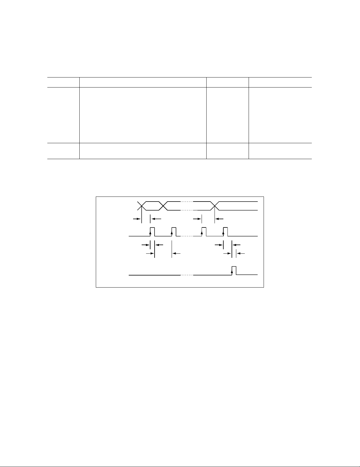
Table 21. R7 VCXO Control Register
Data Sheet I CX74063-26
Symbol Function Description Internal Power-
On Value
(Binary)
Recommended
Operational Value
(Binary)
ADDR Address bits [6:0]. Must be set to 1101101b (see Table 12)
I_VCXO Bit [10:7] negative resistance current control. Binary
0101 1001
weighted.
Negative logic (on = low, off = high)
Bit [10] = LSB = 8 µA
Bit [7] = MSB = 64 µA
Stepped values = 64 µA, 32 µA, 16 µA, 8 µA
RSVD Bit [23:11] reserved. Must be set to default value. 0000000000000 0000000001110
(Must Use)
Note: Programmed values in this register are not maintained with VDDBB (pin 43).
DATA
t
CS
S0S1S22S23
t
CH
CLOCK
LE
t
CWH
t
CWL
t
ES
Figure 9. Serial Data Input Timing Diagram For Transceiver
t
EW
C898
Skyworks Solutions, Inc., Proprietary and Confidential 37
103052A [781] 376-3000 I FAX [781] 376-3100 I SALES@SKYWORKSINC.COM I WWW.SKYWORKSINC.COM MAY 16, 2003
Page 38
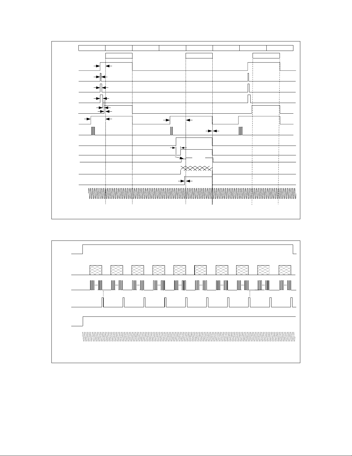
Data Sheet I CX74063-26
7
0
1
RX
RXENA
Internal DCOC 1
Internal DCOC 2
Internal DCOC 3
Internal FEENA
SXENA
LE
TXENA
OFFSET GEN TIMING
PAVAPC
TX I/Q
TRSW Enable
FREF
(not to scale)
Note 1: This timing depends on circuitry other than the CX74063.
120 µs
20 µs
40 µs
60 µs
10 µs
50 µs
240 µs
240 µs
25 µs (Note 1)
PAC_TIME
2
0.7 V
3
TX
10 µs (Note 1)
PA RAMP
Voltage
4
5
6
Mon
C1330
Figure 10. CX74063-26 Signal Timing Example (Normal Operation)
SXENA
Preset=1
DATA
CLK
LE
VDDBB
(pin 43)
FREF
(not to scale)
Note 1. LE should be low before the next clock goes high.
Note 2. VDDBB, pin 43, is required to hold the register settings. If VDDBB is not maintained high, the power-on
Note 2
programming sequence needs to be added in front of each normal slot programming sequence.
Preset=0
Band=GSM
Note 1
GSM
IP2 I
GSM
IP2 Q
Preset=0
Band=DCS/PCS
DCS/PCS
IP2 I
DCS/PCS
IP2 Q
DCOC
timing
Control 1
Note 1
VCXO
VCXO
Control 2
C1329
Figure 11. CX74063-26 Register Programming Sequence and Timing Example (Initialization After Power Up)
38 Skyworks Solutions, Inc., Proprietary and Confidential
MAY 16, 2003 [781] 376-3000 I FAX [781] 376-3100 I SALES@SKYWORKSINC.COM I WWW.SKYWORKSINC.COM 103052A
Page 39

Receiver Data
Data Sheet I CX74063-26
Table 22. Recommended EGSM900/GSM850 AGC Data (1 of 2)
(AGC Setpoint = - 25.2 dBV = 55.0 mVrms)
(dB)
Internal
Interstage
Losses
(dB)
Total
voltage
Gain
(dB)
I/Q Output
(dBV)
From To
Antenna Input
(dBm)
From To
External
Front
End
Losses
LNA
(dB)
Mixer
(dB)
LPF
(dB)
VGA1
(dB)
VGA1
Fine (dB)
Aux
(dB)
VGA2
(dB)
–110 –108 –4.0 15 40 10 18 4 0 18 –4.2 96.8 –26.2 –24.2
–108 –106 –4.0 15 40 10 18 2 0 18 –4.2 94.8 –26.2 –24.2
–106 –104 –4.0 15 40 10 18 0 0 18 –4.2 92.8 –26.2 –24.2
–104 –102 –4.0 15 40 10 12 4 0 18 –4.2 90.8 –26.2 –24.2
–102 –100 –4.0 15 40 10 12 2 0 18 –4.2 88.8 –26.2 –24.2
–100 –98 –4.0 15 40 10 12 0 0 18 –4.2 86.8 –26.2 –24.2
–98 –96 –4.0 15 40 10 6 4 0 18 –4.2 84.8 –26.2 –24.2
–96 –94 –4.0 15 40 10 6 2 0 18 –4.2 82.8 –26.2 –24.2
–94 –92 –4.0 15 40 10 6 0 0 18 –4.2 80.8 –26.2 –24.2
–92 –90 –4.0 15 40 10 0 4 0 18 –4.2 78.8 –26.2 –24.2
–90 –88 –4.0 15 40 10 0 2 0 18 –4.2 76.8 –26.2 –24.2
–88 –86 –4.0 15 40 10 0 0 0 18 –4.2 74.8 –26.2 –24.2
–86 –84 –4.0 15 40 –2 6 4 0 18 –4.2 72.8 –26.2 –24.2
–84 –82 –4.0 15 40 –2 6 2 0 18 –4.2 70.8 –26.2 –24.2
–82 –80 –4.0 15 40 –2 6 0 0 18 –4.2 68.8 –26.2 –24.2
–80 –78 –4.0 15 40 –2 0 4 0 18 –4.2 66.8 –26.2 –24.2
–78 –76 –4.0 15 40 –2 0 2 0 18 –4.2 64.8 –26.2 –24.2
–76 –74 –4.0 15 40 –2 0 0 0 18 –4.2 62.8 –26.2 –24.2
–74 –72 –4.0 15 22 10 0 4 0 18 –4.2 60.8 –26.2 –24.2
–72 –70 –4.0 15 22 10 0 2 0 18 –4.2 58.8 –26.2 –24.2
–70 –68 –4.0 15 22 10 0 0 0 18 –4.2 56.8 –26.2 –24.2
–68 –66 –4.0 15 22 –2 6 4 0 18 –4.2 54.8 –26.2 –24.2
–66 –64 –4.0 15 22 –2 6 2 0 18 –4.2 52.8 –26.2 –24.2
–64 –62 –4.0 15 22 –2 6 0 0 18 –4.2 50.8 –26.2 –24.2
–62 –60 –4.0 15 22 –2 0 4 0 18 –4.2 48.8 –26.2 –24.2
–60 –58 –4.0 15 22 –2 0 2 0 18 –4.2 46.8 –26.2 –24.2
–58 –56 –4.0 15 22 –2 0 0 0 18 –4.2 44.8 –26.2 –24.2
–56 –54 –4.0 –5 22 10 6 0 0 18 –4.2 42.8 –26.2 –24.2
–54 –52 –4.0 –5 22 10 0 4 0 18 –4.2 40.8 –26.2 –24.2
Skyworks Solutions, Inc., Proprietary and Confidential 39
103052A [781] 376-3000 I FAX [781] 376-3100 I SALES@SKYWORKSINC.COM I WWW.SKYWORKSINC.COM MAY 16, 2003
Page 40
Data Sheet I CX74063-26
Table 22. Recommended EGSM900/GSM850 AGC Data (2 of 2)
(AGC Setpoint = - 25.2 dBV = 55.0 mVrms)
(dB)
Internal
Interstage
Losses
(dB)
Total
voltage
Gain
(dB)
I/Q Output
(dBV)
From To
Antenna Input
(dBm)
From To
External
Front
End
Losses
LNA
(dB)
Mixer
(dB)
LPF
(dB)
VGA1
(dB)
VGA1
Fine (dB)
Aux
(dB)
VGA2
(dB)
–52 –50 –4.0 –5 22 10 0 2 0 18 –4.2 38.8 –26.2 –24.2
–50 –48 –4.0 –5 22 10 0 0 0 18 –4.2 36.8 –26.2 –24.2
–48 –46 –4.0 –5 22 –2 6 4 0 18 –4.2 34.8 –26.2 –24.2
–46 –44 –4.0 –5 22 –2 6 2 0 18 –4.2 32.8 –26.2 –24.2
–44 –42 –4.0 –5 22 –2 6 0 0 18 –4.2 30.8 –26.2 –24.2
–42 –40 –4.0 –5 22 –2 0 4 0 18 –4.2 28.8 –26.2 –24.2
–40 –38 –4.0 –5 22 –2 0 2 0 18 –4.2 26.8 –26.2 –24.2
–38 –36 –4.0 –5 22 –2 0 0 0 18 –4.2 24.8 –26.2 –24.2
–36 –34 –4.0 –5 22 –2 0 4 0 12 –4.2 22.8 –26.2 –24.2
–34 –32 –4.0 –5 22 –2 0 2 0 12 –4.2 20.8 –26.2 –24.2
–32 –30 –4.0 –5 22 –2 0 0 0 12 –4.2 18.8 –26.2 –24.2
–30 –28 –4.0 –5 22 –2 0 4 0 6 –4.2 16.8 –26.2 –24.2
–28 –26 –4.0 –5 22 –2 0 2 0 6 –4.2 14.8 –26.2 –24.2
–26 –24 –4.0 –5 22 –2 0 0 0 6 –4.2 12.8 –26.2 –24.2
–24 –22 –4.0 –5 22 –2 0 4 0 0 –4.2 10.8 –26.2 –24.2
–22 –20 –4.0 –5 22 –2 0 2 0 0 –4.2 8.8 –26.2 –24.2
–20 –18 –4.0 –5 22 –2 0 0 0 0 –4.2 6.8 –26.2 –24.2
–18 –16 –4.0 –5 22 –2 0 0 0 0 –4.2 6.8 –24.2 –22.2
–16 –14 –4.0 –5 22 –2 0 0 0 0 –4.2 6.8 –22.2 –20.2
40 Skyworks Solutions, Inc., Proprietary and Confidential
MAY 16, 2003 [781] 376-3000 I FAX [781] 376-3100 I SALES@SKYWORKSINC.COM I WWW.SKYWORKSINC.COM 103052A
Page 41

Table 23. Recommended DCS1800 AGC Data (1 of 2)
(AGC Setpoint = - 24.2 dBV = 61.7 mVrms)
Data Sheet I CX74063-26
(dB)
Internal
Interstage
Losses
(dB)
Total
voltage
Gain
(dB)
I/Q Output
(dBV)
From To
Antenna Input
(dBm)
From To
External
Front
End
Losses
LNA
(dB)
Mixer
(dB)
LPF
(dB)
VGA1
(dB)
VGA1
Fine (dB)
Aux
(dB)
VGA2
(dB)
–110 –108 –4.2 15 40 10 24 0 0 18 –5.0 97.8 –25.2 –23.2
–108 –106 –4.2 15 40 10 18 4 0 18 –5.0 95.8 –25.2 –23.2
–106 –104 –4.2 15 40 10 18 2 0 18 –5.0 93.8 –25.2 –23.2
–104 –102 –4.2 15 40 10 18 0 0 18 –5.0 91.8 –25.2 –23.2
–102 –100 –4.2 15 40 10 12 4 0 18 –5.0 89.8 –25.2 –23.2
–100 –98 –4.2 15 40 10 12 2 0 18 –5.0 87.8 –25.2 –23.2
–98 –96 –4.2 15 40 10 12 0 0 18 –5.0 85.8 –25.2 –23.2
–96 –94 –4.2 15 40 10 6 4 0 18 –5.0 83.8 –25.2 –23.2
–94 –92 –4.2 15 40 10 6 2 0 18 –5.0 81.8 –25.2 –23.2
–92 –90 –4.2 15 40 10 6 0 0 18 –5.0 79.8 –25.2 –23.2
–90 –88 –4.2 15 40 10 0 4 0 18 –5.0 77.8 –25.2 –23.2
–88 –86 –4.2 15 40 10 0 2 0 18 –5.0 75.8 –25.2 –23.2
–86 –84 –4.2 15 40 10 0 0 0 18 –5.0 73.8 –25.2 –23.2
–84 –82 –4.2 15 40 –2 6 4 0 18 –5.0 71.8 –25.2 –23.2
–82 –80 –4.2 15 40 –2 6 2 0 18 –5.0 69.8 –25.2 –23.2
–80 –78 –4.2 15 40 –2 6 0 0 18 –5.0 67.8 –25.2 –23.2
–78 –76 –4.2 15 40 –2 0 4 0 18 –5.0 65.8 –25.2 –23.2
–76 –74 –4.2 15 40 –2 0 2 0 18 –5.0 63.8 –25.2 –23.2
–74 –72 –4.2 15 40 –2 0 0 0 18 –5.0 61.8 –25.2 –23.2
–72 –70 –4.2 15 22 10 0 4 0 18 –5.0 59.8 –25.2 –23.2
–70 –68 –4.2 15 22 10 0 2 0 18 –5.0 57.8 –25.2 –23.2
–68 –66 –4.2 15 22 10 0 0 0 18 –5.0 55.8 –25.2 –23.2
–66 –64 –4.2 15 22 10 6 4 0 18 –5.0 53.8 –25.2 –23.2
–64 –62 –4.2 15 22 –2 6 2 0 18 –5.0 51.8 –25.2 –23.2
–62 –60 –4.2 15 22 –2 6 0 0 18 –5.0 49.8 –25.2 –23.2
–60 –58 –4.2 15 22 –2 0 4 0 18 –5.0 47.8 –25.2 –23.2
–58 –56 –4.2 15 22 –2 0 2 0 18 –5.0 45.8 –25.2 –23.2
–56 –54 –4.2 15 22 –2 0 0 0 18 –5.0 43.8 –25.2 –23.2
–54 –52 –4.2 –7 22 10 6 2 0 18 –5.0 41.8 –25.2 –23.2
–52 –50 –4.2 –7 22 10 6 0 0 18 –5.0 39.8 –25.2 –23.2
Skyworks Solutions, Inc., Proprietary and Confidential 41
103052A [781] 376-3000 I FAX [781] 376-3100 I SALES@SKYWORKSINC.COM I WWW.SKYWORKSINC.COM MAY 16, 2003
Page 42

Data Sheet I CX74063-26
Table 23. Recommended DCS1800 AGC Data (2 of 2)
(AGC Setpoint = - 24.2 dBV = 61.7 mVrms)
(dB)
Internal
Interstage
Losses
(dB)
Total
voltage
Gain
(dB)
I/Q Output
(dBV)
From To
Antenna Input
(dBm)
From To
External
Front
End
Losses
LNA
(dB)
Mixer
(dB)
LPF
(dB)
VGA1
(dB)
VGA1
Fine (dB)
Aux
(dB)
VGA2
(dB)
–50 –48 –4.2 –7 22 10 0 4 0 18 –5.0 37.8 –25.2 –23.2
–48 –46 –4.2 –7 22 10 0 2 0 18 –5.0 35.8 –25.2 –23.2
–46 –44 –4.2 –7 22 10 0 0 0 18 –5.0 33.8 –25.2 –23.2
–44 –42 –4.2 –7 22 –2 6 4 0 18 –5.0 31.8 –25.2 –23.2
–42 –40 –4.2 –7 22 –2 6 2 0 18 –5.0 29.8 –25.2 –23.2
–40 –38 –4.2 –7 22 –2 6 0 0 18 –5.0 27.8 –25.2 –23.2
–38 –36 –4.2 –7 22 –2 0 4 0 18 –5.0 25.8 –25.2 –23.2
–36 –34 –4.2 –7 22 –2 0 2 0 18 –5.0 23.8 –25.2 –23.2
–34 –32 –4.2 –7 22 –2 0 0 0 18 –5.0 21.8 –25.2 –23.2
–32 –30 –4.2 –7 22 –2 0 4 0 12 –5.0 19.8 –25.2 –23.2
–30 –28 –4.2 –7 22 –2 0 2 0 12 –5.0 17.8 –25.2 –23.2
–28 –26 –4.2 -7 22 –2 0 0 0 12 –5.0 15.8 –25.2 –23.2
–26 –24 –4.2 -7 22 –2 0 4 0 6 –5.0 13.8 –25.2 –23.2
–24 –22 –4.2 -7 22 –2 0 2 0 6 –5.0 11.8 –25.2 –23.2
–22 –20 –4.2 -7 22 –2 0 0 0 6 –5.0 9.8 –25.2 –23.2
–20 –18 –4.2 -7 22 –2 0 4 0 0 –5.0 7.8 –25.2 –23.2
–18 –16 –4.2 -7 22 –2 0 2 0 0 –5.0 5.8 –25.2 –23.2
–16 –14 –4.2 -7 22 –2 0 0 0 0 –5.0 5.8 –23.2 –21.2
42 Skyworks Solutions, Inc., Proprietary and Confidential
MAY 16, 2003 [781] 376-3000 I FAX [781] 376-3100 I SALES@SKYWORKSINC.COM I WWW.SKYWORKSINC.COM 103052A
Page 43

Table 24. Recommended PCS1900 AGC Data (1 of 2)
(AGC Setpoint = - 25.4 dBV = 53.7 mVrms)
Data Sheet I CX74063-26
(dB)
Internal
Interstage
Losses
(dB)
Total
voltage
Gain
(dB)
I/Q Output
(dBV)
From To
Antenna Input
(dBm)
From To
External
Front
End
Losses
LNA
(dB)
Mixer
(dB)
LPF
(dB)
VGA1
(dB)
VGA1
Fine (dB)
Aux
(dB)
VGA2
(dB)
–110 –108 –4.2 15 40 10 24 0 0 18 –6.2 96.6 –26.4 –24.4
–108 –106 –4.2 15 40 10 18 4 0 18 –6.2 94.6 –26.4 –24.4
–106 –104 –4.2 15 40 10 18 2 0 18 –6.2 92.6 –26.4 –24.4
–104 –102 –4.2 15 40 10 18 0 0 18 –6.2 90.6 –26.4 –24.4
–102 –100 –4.2 15 40 10 12 4 0 18 –6.2 88.6 –26.4 –24.4
–100 –98 –4.2 15 40 10 12 2 0 18 –6.2 86.6 –26.4 –24.4
–98 –96 –4.2 15 40 10 12 0 0 18 –6.2 84.6 –26.4 –24.4
–96 –94 –4.2 15 40 10 6 4 0 18 –6.2 82.6 –26.4 –24.4
–94 –92 –4.2 15 40 10 6 2 0 18 –6.2 80.6 –26.4 –24.4
–92 –90 –4.2 15 40 10 6 0 0 18 –6.2 78.6 –26.4 –24.4
–90 –88 –4.2 15 40 10 0 4 0 18 –6.2 76.6 –26.4 –24.4
–88 –86 –4.2 15 40 10 0 2 0 18 –6.2 74.6 –26.4 –24.4
–86 –84 –4.2 15 40 10 0 0 0 18 –6.2 72.6 –26.4 –24.4
–84 –82 –4.2 15 40 –2 6 4 0 18 –6.2 70.6 –26.4 –24.4
–82 –80 –4.2 15 40 –2 6 2 0 18 –6.2 68.6 –26.4 –24.4
–80 –78 –4.2 15 40 –2 6 0 0 18 –6.2 66.6 –26.4 –24.4
–78 –76 –4.2 15 40 –2 0 4 0 18 –6.2 64.6 –26.4 –24.4
–76 –74 –4.2 15 40 –2 0 2 0 18 –6.2 62.6 –26.4 –24.4
–74 –72 –4.2 15 40 –2 0 0 0 18 –6.2 60.6 –26.4 –24.4
–72 –70 –4.2 15 22 10 0 4 0 18 –6.2 58.6 –26.4 –24.4
–70 –68 –4.2 15 22 10 0 2 0 18 –6.2 56.6 –26.4 –24.4
–68 –66 –4.2 15 22 10 0 0 0 18 –6.2 54.6 –26.4 –24.4
–66 –64 –4.2 15 22 –2 6 4 0 18 –6.2 52.6 –26.4 –24.4
–64 –62 –4.2 15 22 –2 6 2 0 18 –6.2 50.6 –26.4 –24.4
–62 –60 –4.2 15 22 –2 6 0 0 18 –6.2 48.6 –26.4 –24.4
–60 –58 –4.2 15 22 –2 0 4 0 18 –6.2 46.6 –26.4 –24.4
–58 –56 –4.2 15 22 –2 0 2 0 18 –6.2 44.6 –26.4 –24.4
–56 –54 –4.2 15 22 –2 0 0 0 18 –6.2 42.6 –26.4 –24.4
–54 –52 –4.2 –5 22 10 6 0 0 18 –6.2 40.6 –26.4 –24.4
–52 –50 –4.2 –5 22 10 0 4 0 18 –6.2 38.6 –26.4 –24.4
Skyworks Solutions, Inc., Proprietary and Confidential 43
103052A [781] 376-3000 I FAX [781] 376-3100 I SALES@SKYWORKSINC.COM I WWW.SKYWORKSINC.COM MAY 16, 2003
Page 44

Data Sheet I CX74063-26
Table 24. Recommended PCS1900 AGC Data (2 of 2)
(AGC Setpoint = - 25.4 dBV = 53.7 mVrms)
(dB)
Internal
Interstage
Losses
(dB)
Total
voltage
Gain
(dB)
I/Q Output
(dBV)
From To
Antenna Input
(dBm)
From To
External
Front
End
Losses
LNA
(dB)
Mixer
(dB)
LPF
(dB)
VGA1
(dB)
VGA1
Fine (dB)
Aux
(dB)
VGA2
(dB)
–50 –48 –4.2 –5 22 10 0 2 0 18 –6.2 36.6 –26.4 –24.4
–48 –46 –4.2 –5 22 10 0 0 0 18 –6.2 34.6 –26.4 –24.4
–46 –44 –4.2 –5 22 –2 6 4 0 18 –6.2 32.6 –26.4 –24.4
–44 –42 –4.2 –5 22 –2 6 2 0 18 –6.2 30.6 –26.4 –24.4
–42 –40 –4.2 –5 22 –2 6 0 0 18 –6.2 28.6 –26.4 –24.4
–40 –38 –4.2 –5 22 –2 0 4 0 18 –6.2 26.6 –26.4 –24.4
–38 –36 –4.2 –5 22 –2 0 2 0 18 –6.2 24.6 –26.4 –24.4
–36 –34 –4.2 –5 22 –2 0 0 0 18 –6.2 22.6 –26.4 –24.4
–34 –32 –4.2 –5 22 –2 0 4 0 12 –6.2 20.6 –26.4 –24.4
–32 –30 –4.2 –5 22 –2 0 2 0 12 –6.2 18.6 –26.4 –24.4
–30 –28 –4.2 –5 22 –2 0 0 0 12 –6.2 16.6 –26.4 –24.4
–28 –26 –4.2 –5 22 –2 0 4 0 6 –6.2 14.6 –26.4 –24.4
–26 –24 –4.2 –5 22 –2 0 2 0 6 –6.2 12.6 –26.4 –24.4
–24 –22 –4.2 –5 22 –2 0 0 0 6 –6.2 10.6 –26.4 –24.4
–22 –20 –4.2 –5 22 –2 0 4 0 0 –6.2 8.6 –26.4 –24.4
–20 –18 –4.2 –5 22 –2 0 2 0 0 –6.2 6.6 –26.4 –24.4
–18 –16 –4.2 –5 22 –2 0 0 0 0 –6.2 4.6 –26.4 –24.4
–16 –14 –4.2 –5 22 –2 0 0 0 0 –6.2 4.6 –24.4 –22.4
101514D 10_071101
Figure 12. Typical Baseband Frequency Response
44 Skyworks Solutions, Inc., Proprietary and Confidential
MAY 16, 2003 [781] 376-3000 I FAX [781] 376-3100 I SALES@SKYWORKSINC.COM I WWW.SKYWORKSINC.COM 103052A
Page 45

µsec
Data Sheet I CX74063-26
101514D 11_071101
Figure 13. Typical Differential Delay Response
Table 25. EGSM900/GSM850 LNA S11 (Normalized to 50 Ω)
Frequency (MHz) S11
869.0 0.386 – 0.632j
878.1 0.438 – 0.630j
887.2 0.454 – 0.629j
896.3 0.420 – 0.639j
905.4 0.403 – 0.642j
914.5 0.398 – 0.646j
923.6 0.371 – 0.653j
932.7 0.376 – 0.653j
941.8 0.379 – 0.657j
950.9 0.343 – 0.664j
960.0 0.350 – 0.664j
Skyworks Solutions, Inc., Proprietary and Confidential 45
103052A [781] 376-3000 I FAX [781] 376-3100 I SALES@SKYWORKSINC.COM I WWW.SKYWORKSINC.COM MAY 16, 2003
Page 46

Data Sheet I CX74063-26
Table 26. DCS1800 LNA S11 (Normalized to 50 Ω)
Frequency (MHz) S11
1805.0 0.0205 – 0.649j
1812.5 0.205 – 0.689j
1820.0 0.275 – 0.704j
1827.5 0.299 – 0.710j
1835.0 0.319 – 0.713j
1842.5 0.326 – 0.718j
1850.0 0.316 – 0.722j
1857.5 0.306 – 0.722j
1865.0 0.307 – 0.722j
1872.5 0.300 – 0.724j
1880.0 0.287 – 0.724j
Table 27. PCS1900 LNA S11 (Normalized to 50 Ω)
Frequency (MHz) S11
1930 0.237 – 0.583j
1936 0.362 – 0.595j
1942 0.432 – 0.591j
1948 0.472 – 0.589j
1954 0.489 – 0.591j
1960 0.488 – 0.597j
1966 0.483 – 0.600j
1972 0.485 – 0.600j
1978 0.484 – 0.600j
1984 0.475 – 0.603j
1990 0.465 – 0.605j
46 Skyworks Solutions, Inc., Proprietary and Confidential
MAY 16, 2003 [781] 376-3000 I FAX [781] 376-3100 I SALES@SKYWORKSINC.COM I WWW.SKYWORKSINC.COM 103052A
Page 47

Data Sheet I CX74063-26
Table 28. Typical EGSM and GSM850 Band Noise Figure vs. Gain Data
Gain NF Gain NF Gain NF Gain NF Gain NF Gain NF
100.8 3.17 84.8 3.38 68.8 7.60 52.8 22.50 36.8 39.71 20.8 43.56
98.8 3.17 82.8 3.48 66.8 8.39 50.8 23.76 34.8 41.11 18.8 45.01
96.8 3.17 80.8 3.59 64.8 11.80 48.8 24.92 32.8 42.46 16.8 46.39
94.8 3.18 78.8 3.73 62.8 12.77 46.8 30.21 30.8 43.73 14.8 45.89
92.8 3.20 76.8 4.90 60.8 13.71 44.8 31.29 28.8 44.89 12.8 47.58
90.8 3.22 74.8 5.44 58.8 18.43 42.8 32.37 26.8 42.70 10.8 49.25
88.8 3.26 72.8 6.08 56.8 19.79 40.8 33.39 24.8 44.02
86.8 3.31 70.8 6.82 54.8 21.16 38.8 38.32 22.8 45.24
60.00
50.00
40.00
30.00
Noise Figure (dB)
20.00
10.00
0.00
0 20 40 60 80 100 120
RX Voltage Gain (dB)
101514F 15_111201
Figure 14. Typical EGSM and GSM850 Band Noise Figure vs. Voltage Gain Curve
(CX74063-26 Only, No Front End Loss)
Skyworks Solutions, Inc., Proprietary and Confidential 47
103052A [781] 376-3000 I FAX [781] 376-3100 I SALES@SKYWORKSINC.COM I WWW.SKYWORKSINC.COM MAY 16, 2003
Page 48

Data Sheet I CX74063-26
Table 29. Typical EGSM and GSM850 Band Dynamic Range Data (Includes 4.0 dB Front End Loss)
Input Noise
Floor
P1dB Gain Input Noise
Floor
P1dB Gain Input Noise
Floor
P1dB Gain
–109.0 –113.0 –78.6 97.8 –77.0 –108.2 –52.4 65.8 –45.0 –78.6 –21.2 33.8
–107.0 –113.0 –76.6 95.8 –75.0 –107.1 –52.0 63.8 –43.0 –74.5 –18.1 31.8
–105.0 –113.0 –74.6 93.8 –73.0 –106.0 –51.8 61.8 –41.0 –72.9 –17.7 29.8
–103.0 –113.0 –72.6 91.8 –71.0 –102.9 –43.4 59.8 –39.0 –71.4 –17.4 27.8
–101.0 –113.0 –70.6 89.8 –69.0 –101.6 –42.5 57.8 –37.0 –69.8 –17.2 25.8
–99.0 –113.0 –68.7 87.8 –67.0 –100.4 –41.9 55.8 –35.0 –68.3 –17.0 23.8
–97.0 –112.9 –66.9 85.8 –65.0 –96.4 –36.9 53.8 –33.0 –66.9 –17.0 21.8
–95.0 –112.9 –65.2 83.8 –63.0 –94.9 –35.9 51.8 –31.0 –66.9 –16.9 19.8
–93.0 –112.8 –63.7 81.8 –61.0 –93.4 –35.2 49.8 –29.0 –65.2 –16.9 17.8
–91.0 –112.7 –62.4 79.8 –59.0 –91.8 –34.6 47.8 –27.0 –63.4 –16.9 15.8
–89.0 –112.5 –61.4 77.8 –57.0 –90.3 –34.3 45.8 –25.0 –62.3 –16.8 13.8
–87.0 –112.3 –60.5 75.8 –55.0 –88.9 –34.0 43.8 –23.0 –60.3 –16.8 11.8
–85.0 –112.1 –59.9 73.8 –53.0 –83.8 –24.3 41.8 –21.0 –58.4 –16.8 9.8
–83.0 –110.8 –54.8 71.8 –51.0 –82.6 –23.2 39.8 –19.0 –56.7 –16.8 7.8
–81.0 –110.0 –53.8 69.8 –49.0 –81.3 –22.3 37.8 –17.0 –54.7 –16.8 5.8
–79.0 –109.2 –53.0 67.8 –47.0 –79.9 –21.7 35.8 –15.0 –52.7 –16.8 3.8
-10.00
-20.00
P1dB
-40.00
-60.00
dBm
Input
-80.00
Noise Floor
-100.00
-120.00
-120.0 -100.0 -80.0
+ 4.0 dB Front End Loss
-60.0 -40.0 -20.0 0.0
Antenna Input (dBm)
101514F 16_111901
Figure 15. Typical EGSM and GSM850 Band Dynamic Range vs. Antenna Input Curve
48 Skyworks Solutions, Inc., Proprietary and Confidential
MAY 16, 2003 [781] 376-3000 I FAX [781] 376-3100 I SALES@SKYWORKSINC.COM I WWW.SKYWORKSINC.COM 103052A
Page 49
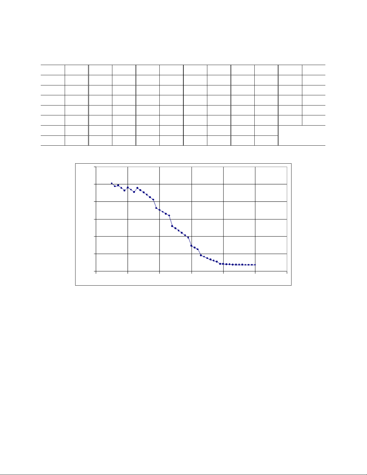
Data Sheet I CX74063-26
Table 30. Typical DCS1800 Band Noise Figure vs. Gain Data
Gain NF Gain NF Gain NF Gain NF Gain NF Gain NF
100 3.7 84 3.9 68 8.3 52 23.3 36 41.1 20 48.0
98 3.7 82 4.0 66 9.1 50 24.6 34 42.5 18 46.4
96 3.7 80 4.1 64 12.6 48 25.7 32 43.9 16 47.8
94 3.7 78 4.3 62 13.6 46 32.0 30 45.3 14 49.2
92 3.7 76 5.5 60 14.5 44 33.0 28 46.5 12 48.7
90 3.7 74 6.1 58 19.2 42 34.1 26 47.7 10 50.4
88 3.8 72 6.7 56 20.6 40 35.2 24 45.5
86 3.8 70 7.5 54 22.0 38 36.2 22 46.8
60.00
50.00
40.00
30.00
Noise Figure (dB)
20.00
10.00
0.00
0 20 40 60 80 100 120
RX Voltage Gain (dB)
101514F 17_111201
Figure 16. Typical DCS1800 Band Noise Figure vs. Voltage Gain Curve
(CX74063-26 Only; No Front End Loss)
Skyworks Solutions, Inc., Proprietary and Confidential 49
103052A [781] 376-3000 I FAX [781] 376-3100 I SALES@SKYWORKSINC.COM I WWW.SKYWORKSINC.COM MAY 16, 2003
Page 50

Data Sheet I CX74063-26
Table 31. Typical DCS1800 Band Dynamic Range Data (Includes 4.2 dB Front End Loss)
Input Noise
Floor
P1dB Gain Input Noise
Floor
P1dB Gain Input Noise
Floor
P1dB Gain
–109.0 –113.0 –78.6 97.8 –77.0 –108.2 –52.4 65.8 –45.0 –78.6 –21.2 33.8
–107.0 –113.0 –76.6 95.8 –75.0 –107.1 –52.0 63.8 –43.0 –74.5 –18.1 31.8
–105.0 –113.0 –74.6 93.8 –73.0 –106.0 –51.8 61.8 –41.0 –72.9 –17.7 29.8
–103.0 –113.0 –72.6 91.8 –71.0 –102.9 –43.4 59.8 –39.0 –71.4 –17.4 27.8
–101.0 –113.0 –70.6 89.8 –69.0 –101.6 –42.5 57.8 –37.0 –69.8 –17.2 25.8
–99.0 –113.0 –68.7 87.8 –67.0 –100.4 –41.9 55.8 –35.0 –68.3 –17.0 23.8
–97.0 –112.9 –66.9 85.8 –65.0 –96.4 –36.9 53.8 –33.0 –66.9 –17.0 21.8
–95.0 –112.9 –65.2 83.8 –63.0 –94.9 –35.9 51.8 –31.0 –66.9 –16.9 19.8
–93.0 –112.8 –63.7 81.8 –61.0 –93.4 –35.2 49.8 –29.0 –65.2 –16.9 17.8
–91.0 –112.7 –62.4 79.8 –59.0 –91.8 –34.6 47.8 –27.0 –63.4 –16.9 15.8
–89.0 –112.5 –61.4 77.8 –57.0 –90.3 –34.3 45.8 –25.0 –62.3 –16.8 13.8
–87.0 –112.3 –60.5 75.8 –55.0 –88.9 –34.0 43.8 –23.0 –60.3 –16.8 11.8
–85.0 –112.1 –59.9 73.8 –53.0 –83.8 –24.3 41.8 –21.0 –58.4 –16.8 9.8
–83.0 –110.8 –54.8 71.8 –51.0 –82.6 –23.2 39.8 –19.0 –56.7 –16.8 7.8
–81.0 –110.0 –53.8 69.8 –49.0 –81.3 –22.3 37.8 –17.0 –54.7 –16.8 5.8
–79.0 –109.2 –53.0 67.8 –47.0 –79.9 –21.7 35.8 –15.0 –52.7 –16.8 3.8
-10.00
-20.00
P1dB
-40.00
-60.00
dBm
Input
-80.00
Noise Floor
-100.00
-120.00
-120.0 -100.0 -80.0
+ 4.2 dB Front End Loss
-60.0 -40.0 -20.0 0.0
Antenna Input (dBm)
101514F 18_111201
Figure 17. Typical DCS1800 Band Dynamic Range vs. Antenna Input Curve
50 Skyworks Solutions, Inc., Proprietary and Confidential
MAY 16, 2003 [781] 376-3000 I FAX [781] 376-3100 I SALES@SKYWORKSINC.COM I WWW.SKYWORKSINC.COM 103052A
Page 51
Data Sheet I CX74063-26
Table 32. Typical PCS1900 Band Noise Figure vs. Gain Data
Gain NF Gain NF Gain NF Gain NF Gain NF Gain NF
98.8 4.2 82.8 4.5 66.8 9.3 50.8 24.5 34.8 42.3 18.8 49.2
96.8 4.2 80.8 4.6 64.8 10.1 48.8 25.8 32.8 43.7 16.8 47.6
94.8 4.2 78.8 4.7 62.8 13.7 46.8 26.9 30.8 45.1 14.8 49.0
92.8 4.2 76.8 4.9 60.8 14.7 44.8 33.2 28.8 46.5 12.8 50.4
90.8 4.2 74.8 6.3 58.8 15.6 42.8 34.2 26.8 47.7 10.8 49.9
88.8 4.3 72.8 6.9 56.8 20.4 40.8 35.3 24.8 48.9 8.8 51.6
86.8 4.3 70.8 7.6 54.8 21.8 38.8 36.4 22.8 46.7 6.8 53.3
84.8 4.4 68.8 8.4 52.8 23.1 36.8 37.4 20.8 48.0
60.00
50.00
40.00
30.00
Noise Figure (dB)
20.00
10.00
0.00
0 20 40 60 80 100 120
RX Voltage Gain (dB)
101514F 19_111901
Figure 18. Typical PCS1900 Band Noise Figure vs. Voltage Gain Curve
(CX74063-26 Only; No Front End Loss)
Skyworks Solutions, Inc., Proprietary and Confidential 51
103052A [781] 376-3000 I FAX [781] 376-3100 I SALES@SKYWORKSINC.COM I WWW.SKYWORKSINC.COM MAY 16, 2003
Page 52

Data Sheet I CX74063-26
Table 33. Typical PCS1900 Band Dynamic Range Data (Includes 4.2 dB Front End Loss)
Input Noise
Floor
P1dB Gain Input Noise
Floor
P1dB Gain Input Noise
Floor
P1dB Gain
–109.0 –112.5 –77.4 96.6 –77.0 –107.4 –51.2 64.6 –45.0 –77.7 –20.3 32.6
–107.0 –112.5 –75.4 94.6 –75.0 –106.3 –50.8 62.6 –43.0 –73.5 –17.6 30.6
–105.0 –112.5 –73.4 92.6 –73.0 –105.2 –50.6 60.6 –41.0 –72.0 –17.2 28.6
–103.0 –112.5 –71.4 90.6 –71.0 –102.0 –42.2 58.6 –39.0 –70.4 –17.0 26.6
–101.0 –112.5 –69.4 88.6 –69.0 –100.7 –41.3 56.6 –37.0 –68.9 –16.8 24.6
–99.0 –112.5 –67.5 86.6 –67.0 –99.5 –40.7 54.6 –35.0 –67.4 –16.7 22.6
–97.0 –112.4 –65.7 84.6 –65.0 –95.4 –35.7 52.6 –33.0 –66.0 –16.6 20.6
–95.0 –112.4 –64.0 82.6 –63.0 –93.9 –34.7 50.6 –31.0 –66.3 –16.6 18.6
–93.0 –112.3 –62.5 80.6 –61.0 –92.4 –34.0 48.6 –29.0 –64.6 –16.5 16.6
–91.0 –112.1 –61.2 78.6 –59.0 –90.9 –33.4 46.6 –27.0 –62.9 –16.5 14.6
–
89.0 –112.0 –60.2 76.6 –57.0 –89.4 –33.1 44.6 –25.0 –61.8 –16.5 12.6
–87.0 –111.8 –59.3 74.6 –55.0 –88.0 –32.8 42.6 –23.0 –59.9 –16.5 10.6
–85.0 –111.5 –58.7 72.6 –53.0 –82.8 –23.3 40.6 –21.0 –58.0 –16.5 8.6
–83.0 –110.0 –53.6 70.6 –51.0 –81.6 –22.2 38.6 –19.0 –56.3 –16.5 6.6
–81.0 –109.3 –52.6 68.6 –49.0 –80.3 –21.4 36.6 –17.0 –54.3 –16.5 4.6
–79.0 –108.4 –51.8 66.6 –47.0 –79.0 –20.8 34.6 –15.0 –52.4 –16.5 2.6
-10.00
-20.00
P1dB
-40.00
-60.00
dBm
Input
-80.00
Noise Floor
-100.00
-120.00
-120.0 -100.0 -80.0
+4.2 dB Front End Loss
-60.0 -40.0 -20.0 0.0
Antenna Input (dBm)
101514F 20_111901
Figure 19. Typical PCS1900 Band Dynamic Range vs. Antenna Input Curve
52 Skyworks Solutions, Inc., Proprietary and Confidential
MAY 16, 2003 [781] 376-3000 I FAX [781] 376-3100 I SALES@SKYWORKSINC.COM I WWW.SKYWORKSINC.COM 103052A
Page 53
50
45
40
35
30
25
20
15
Typical
10
Control Sensitivity (MHz/V)
Performance
5
0
1100 1200 1300 1400 1500 1600
Specification Limits
VCO Frequency (MHz)
101514F 21_111901
Figure 20. Typical Control Sensitivity, UHF VCO
35
30
Data Sheet I CX74063-26
25
20
15
Typical
Performance
10
Control Sensitivity (MHz/V)
5
0
750 800 850 900 950
VCO Frequency (MHz)
Specification Limits
101514F 22_111901
Figure 21. Typical Control Sensitivity, Low Band TX VCO
30
25
20
15
10
Typical
Performance
Specification Limits
Control Sensitivity (MHz/V)
5
0
1600 1700 1800 1900 2000
1650 1750 1850 1950
VCO Frequency (MHz)
101514F 23_111901
Figure 22. Typical Control Sensitivity, High Band TX VCO
Skyworks Solutions, Inc., Proprietary and Confidential 53
103052A [781] 376-3000 I FAX [781] 376-3100 I SALES@SKYWORKSINC.COM I WWW.SKYWORKSINC.COM MAY 16, 2003
Page 54
Data Sheet I CX74063-26
Transmitter Data
Figure 23. Typical GSM850 Band Output Spectrum
Figure 24. Typical EGSM Band Output Spectrum
54 Skyworks Solutions, Inc., Proprietary and Confidential
MAY 16, 2003 [781] 376-3000 I FAX [781] 376-3100 I SALES@SKYWORKSINC.COM I WWW.SKYWORKSINC.COM 103052A
Page 55

Data Sheet I CX74063-26
Figure 25. Typical DCS Band Output Spectrum
Figure 26. Typical PCS Band Output Spectrum
Skyworks Solutions, Inc., Proprietary and Confidential 55
103052A [781] 376-3000 I FAX [781] 376-3100 I SALES@SKYWORKSINC.COM I WWW.SKYWORKSINC.COM MAY 16, 2003
Page 56
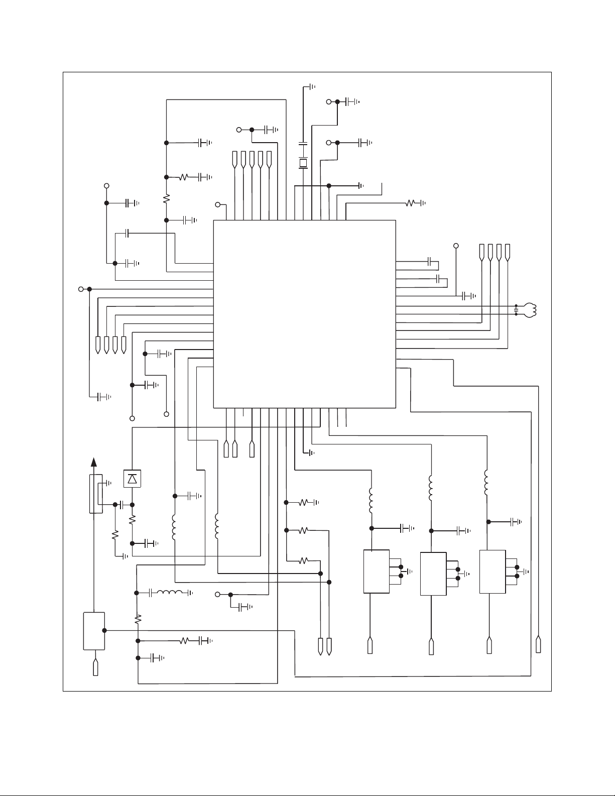
Data Sheet I CX74063-26
VSYN
C26
1 nF
R1
C27
0.1 µF
C4
1 µF
+
V_RF
RXIP
RXIN
RXQP
RXQN
C1475
V_RF
C13
0.1µF
C5
680 pF
VSYN
C11
1 nF
1000 pF
V_RF
VLogic
C7
8.2 nF
LE
CLK
R2
2 kΩ
5.6 kΩ
C2
220 pF
44
45
46
47
48
49
50
51
52
53
54
55
C3
1 nF
56
DATA
4342414039
LE
CLK
DATA
VDDBB
UHFBYP
UHFTUNE
VCCUHF
VCC3
RXQN
RXQP
RXIN
RXIP
VCC4
VCCTXVCO
TX900
XTAL TUNE
XTAL TUNE
TX1800/TX1900
TXVCO TUNE
Crystal
SXENA
38
373635343332313029
XTAL
VCCF
GNDFN
VCCD
SXENA
UHFCPO
VCCFN_CP
Tri-Band
CX74063-26
GSM Transceiver
GNDD
XTAL BUF
C14
LPFADJ
0.1µF
To Baseband
R7
39 kΩ
CAPQN
28
CAPQP
27
CAPIN
26
CAPIP
25
VCC2
24
TXIFN
23
TXIFP
22
TXQN
21
TXQP
20
TXIN
19
TXIP
18
BBVAPC
17
PAVAPC
16
C16
470 pF
C15
V_RF
470 pF
C22
100 nF
TxQN
TxQP
TxIN
TxIP
22 pF
82 nH
C1
100 nF
To Antenna
Coupler
RF out
PA
RF in
V_RF
R3
PAVAPC
270 Ω
C25
1 nF
RF
C8
C17
V_RF
Detector
L4
10 nH
L6
39 pF
39 pF
220 nH
R6
C28
680 Ω
1.8 pF
C18
V_RF
3.9 nF
RXENA
1
L5
TXENA
234
TXENA
RXENA
1.5 nH
C12
PCO
VCXO_EN
VCXO_EN
1 nF
VCC1
PDETVCC
5
6
7
TXINP
TXCPO
9
8
LNA1800IN
PDET
LNA1900IN
GNDLNA900
LNA900IN
13
11
12
10
R8
50 Ω
R4
510 Ω
R5
390 Ω
DCS/PCS TX to PA
NC
NC
14
15
5
F1 GSM SAW
2
GSM TX to PA
L1
10 nH
C21
6
4
OUT
3
1
GROUND
IN
GSM RX input
L2
6.8 nH
1.2 pF
5
F3 DCS SAW
2
DCS RX input
OUT
IN
C23
0.5 pF
6
4
3
1
GROUND
L3
3.3 nH
5
OUT
GROUND
IN
F2 PCS SAW
2
PCS RX input
C24
1.0 pF
6
4
3
1
PAVAPC
BBVAPC
Figure 27. Typical CX74063-26 Application Circuit
56 Skyworks Solutions, Inc., Proprietary and Confidential
MAY 16, 2003 [781] 376-3000 I FAX [781] 376-3100 I SALES@SKYWORKSINC.COM I WWW.SKYWORKSINC.COM 103052A
Page 57
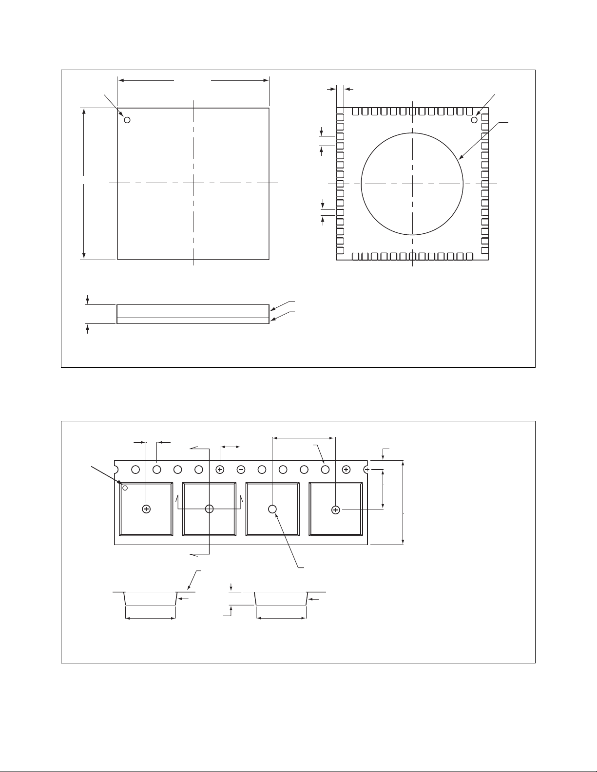
Data Sheet I CX74063-26
e
Pin 1
8.00 ± 0.10
1.00 ± 0.10
All dimensions are in millimeters
8.00 ± 0.10
Top View
Side View
0.38 ± 0.08
Pin 1
R 2.70
0.50
0.30 ± 0.05
Bottom View
Mold
Substrate
C1339
Figure 28. CX74063-26 56-Pin RFLGA Package Dimension Drawing
12.00 ± 0.10
1.50 ± 0.10
8.40 ± 0.10
1.50 ± 0.25
7˚ Max
1.75 ± 0.10
7.50 ± 0.10
16.00 + 0.30/–0.10
Notes:
1. Carrier tape material: black conductive polycarbonat
2. Cover tape material: transparent conductive PSA
3. Cover tape size: 13.3 mm width
4. All measurements are in millimeters
S109
Pin #1
indicator
2.00 ± 0.10
4.00 ± 0.10
B
A
A
B
0.318 ± .02
8˚ Max
8.40 ± 0.10
1.73 ± 0.10
AB
Figure 29. CX74063-26 56-Pin RFLGA Tape and Reel Dimensions
Skyworks Solutions, Inc., Proprietary and Confidential 57
103052A [781] 376-3000 I FAX [781] 376-3100 I SALES@SKYWORKSINC.COM I WWW.SKYWORKSINC.COM MAY 16, 2003
Page 58

Data Sheet I CX74063-26
Ordering Information
CX74063 CX74063-26
Model Name Manufacturing Part Number Product Revision
© 2001, 2002, 2003 Skyworks Solutions, Inc. All Rights Reserved.
Information in this document is provided in connection with Skyworks Solutions, Inc. ("Skyworks") products. These materials are provided by Skyworks as a service to its
customers and may be used for informational purposes only. Skyworks assumes no responsibility for errors or omissions in these materials. Skyworks may make changes
to its products, specifications and product descriptions at any time, without notice. Skyworks makes no commitment to update the information and shall have no
responsibility whatsoever for conflicts, incompatibilities, or other difficulties arising from future changes to its products and product descriptions.
No license, express or implied, by estoppel or otherwise, to any intellectual property rights is granted by this document. Except as may be provided in Skyworks’ Terms
and Conditions of Sale for such products, Skyworks assumes no liability whatsoever.
THESE MATERIALS ARE PROVIDED "AS IS" WITHOUT WARRANTY OF ANY KIND, EITHER EXPRESS OR IMPLIED, RELATING TO SALE AND/OR USE OF SKYWORKS™
PRODUCTS INCLUDING WARRANTIES RELATING TO FITNESS FOR A PARTICULAR PURPOSE, MERCHANTABILITY, PERFORMANCE, QUALITY OR NON-INFRINGEMENT OF ANY
PATENT, COPYRIGHT OR OTHER INTELLECTUAL PROPERTY RIGHT. SKYWORKS FURTHER DOES NOT WARRANT THE ACCURACY OR COMPLETENESS OF THE INFORMATION,
TEXT, GRAPHICS OR OTHER ITEMS CONTAINED WITHIN THESE MATERIALS. SKYWORKS SHALL NOT BE LIABLE FOR ANY SPECIAL, INDIRECT, INCIDENTAL, OR
CONSEQUENTIAL DAMAGES, INCLUDING WITHOUT LIMITATION, LOST REVENUES OR LOST PROFITS THAT MAY RESULT FROM THE USE OF THESE MATERIALS.
Skyworks™ products are not intended for use in medical, lifesaving or life-sustaining applications. Skyworks’ customers using or selling Skyworks™ products for use in
such applications do so at their own risk and agree to fully indemnify Skyworks for any damages resulting from such improper use or sale.
The following are trademarks of Skyworks Solutions, Inc.: Skyworks™, the Skyworks symbol, “Single Package Radio”™, SPR™, and “Breakthrough Simplicity”™.
Product names or services listed in this publication are for identification purposes only, and may be trademarks of third parties. Third-party brands and names are the
property of their respective owners.
GSM™, “Global System for Mobile Communications™,” and the GSM logo are trademarks of the GSM Association. RFLGA™ is a trademark of Conexant Systems, Inc.
Additional information, posted at www.skyworksinc.com, is incorporated by reference.
58 Skyworks Solutions, Inc., Proprietary and Confidential
MAY 16, 2003 [781] 376-3000 I FAX [781] 376-3100 I SALES@SKYWORKSINC.COM I WWW.SKYWORKSINC.COM 103052A
Page 59

General Information
Skyworks Solutions, Inc.
www.skyworksinc.com
20 Sylvan Rd.
Woburn, MA 01801
 Loading...