

Page 1

Bluetooth Module
Module SKB369
Revision
Description
Approved
Date
V1.01
Initial Release
Hogan
20170103
V1.02
Revise The Product Picture
Hogan
20170414
V1.03
Revise Operating Temperature
Hogan
20170421
V1.04
Add Ordering Information
Revise The Product Picture
Abner
20170801
V1.05
Revise PIN 23 function
George
20170821
V1.06
Update certification information
George
20170831
Skylab M&C Technology Co., Ltd
SKB369 Bluetooth
Module
Name: Bluetooth Module
Model No.: SKB369
Revision: V1.06
Revision History
SKB369-DA-001,A/1
Page 2

Module SKB369
Bluetooth Module
Skylab M&C Technology Co., Ltd
Contents
1. General Description ...................................................................................................................................................................................... 4
2. Applications ..................................................................................................................................................................................................... 4
3. Features ............................................................................................................................................................................................................ 4
4. Application Block Diagram ......................................................................................................................................................................... 5
5. Interfaces .......................................................................................................................................................................................................... 6
5.1 Power Supply ...................................................................................................................................................................................... 6
5.2 System Function Interfaces ............................................................................................................................................................. 6
5.2.1 GPIOs ......................................................................................................................................................................................... 6
5.2.2 Two-wire Interface (I2C Compatible) ............................................................................................................................. 6
5.2.3 Flash Program I/Os ............................................................................................................................................................... 7
5.2.4 Serial Peripheral Interface .................................................................................................................................................. 7
5.2.5 UARTs ........................................................................................................................................................................................ 8
5.2.6 Analog to Digital Converter (ADC) .................................................................................................................................. 8
5.2.7 Low Power Comparator (LPCOMP) ................................................................................................................................. 8
5.2.8 Reset .......................................................................................................................................................................................... 9
5.2.9 NFC ............................................................................................................................................................................................ 9
6. Module Specifications ................................................................................................................................................................................ 10
7. Module Pinout and Pin Description ...................................................................................................................................................... 11
7.1 Module Pinout .................................................................................................................................................................................. 11
7.2 Pin Description .................................................................................................................................................................................. 12
8. PCB Design Guide ....................................................................................................................................................................................... 13
9. PCB Footprint and Dimensions ............................................................................................................................................................... 13
10. Electrical Characteristics .......................................................................................................................................................................... 14
10.1 Absolute Maximum Ratings ....................................................................................................................................................... 14
10.2 Recommended Operation Ratings .......................................................................................................................................... 14
SKB369-DA-001,A/1
Page 3

Module SKB369
Bluetooth Module
Skylab M&C Technology Co., Ltd
10.3 Current .............................................................................................................................................................................................. 14
11. Manufacturing Process Recommendations ..................................................................................................................................... 15
12. Packaging Specification .......................................................................................................................................................................... 16
13. Ordering Information .............................................................................................................................................................................. 16
14. Contact Information ................................................................................................................................................................................. 17
SKB369-DA-001,A/1
Page 4
Module SKB369
1. General Description
The SKB369 is a highly integrated Bluetooth 4.2
BLE module, designed for high data rate,
short-range wireless communication in the
2.4GHz ISM band. Also, SKB369 support ANT
Protocol. The module is based on Nordic
nRF52832 radio Transceiver IC, has a 32 bit ARM
Cortex-M4F CPU, Flash memory and analog and
digital peripherals. The SKB369 provides a low
power and ultra-low cost BLE solution for
wireless transmission applications. The SKB369
also has a NFC-A tag interface for OOB pairing.
2. Applications
◆ Computer peripherals and I/O devices
Mouse
Keyboard
Multi-touch trackpad
◆Interactive entertainment devices
Remote control
3D Glasses
Gaming controller
◆Personal Area Networks
Health/fitness sensor and monitor devices
Medical devices
Key-fobs + wrist watches
◆Remote control toys
◆Beacons
◆Bluetooth Gateway
◆Indoor Location
◆Colourful LED Control
3. Features
◆Main Chip: nRF52832
◆Bluetooth® 4.2 low energy single-mode
Bluetooth Module
Skylab M&C Technology Co., Ltd
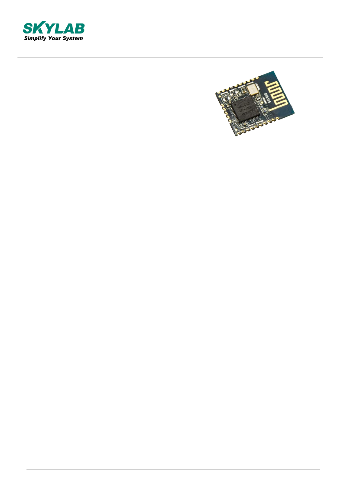
Figure 1: SKB369 Without Shielding Top View
protocol stack
L2CAP, ATT, GAP, GATT and SM protocols
Central and Peripheral roles
GATT Client and Server
Full SMP support including MITM and OOB
pairing
◆Support ANT Protocol
◆Supported data rates up to 1Mbps
◆Support NFC-A
◆8/10/12 bit ADC-6configurable channels
◆19 General Purpose I/O pins
◆SPI Master/Slave
◆Two-wire Master (I2C compatible)
◆UART (CTS/RTS)
◆CPU independent Programmable Peripheral
Interconnect (PPI)
◆Quadrature Decoder (QDEC)
◆AES HW encryption
◆RoHS compliance (Lead-free)
◆FCC,CE compliance
SKB369-DA-001,A/1
Page 5
Module SKB369
Bluetooth Module
Skylab M&C Technology Co., Ltd
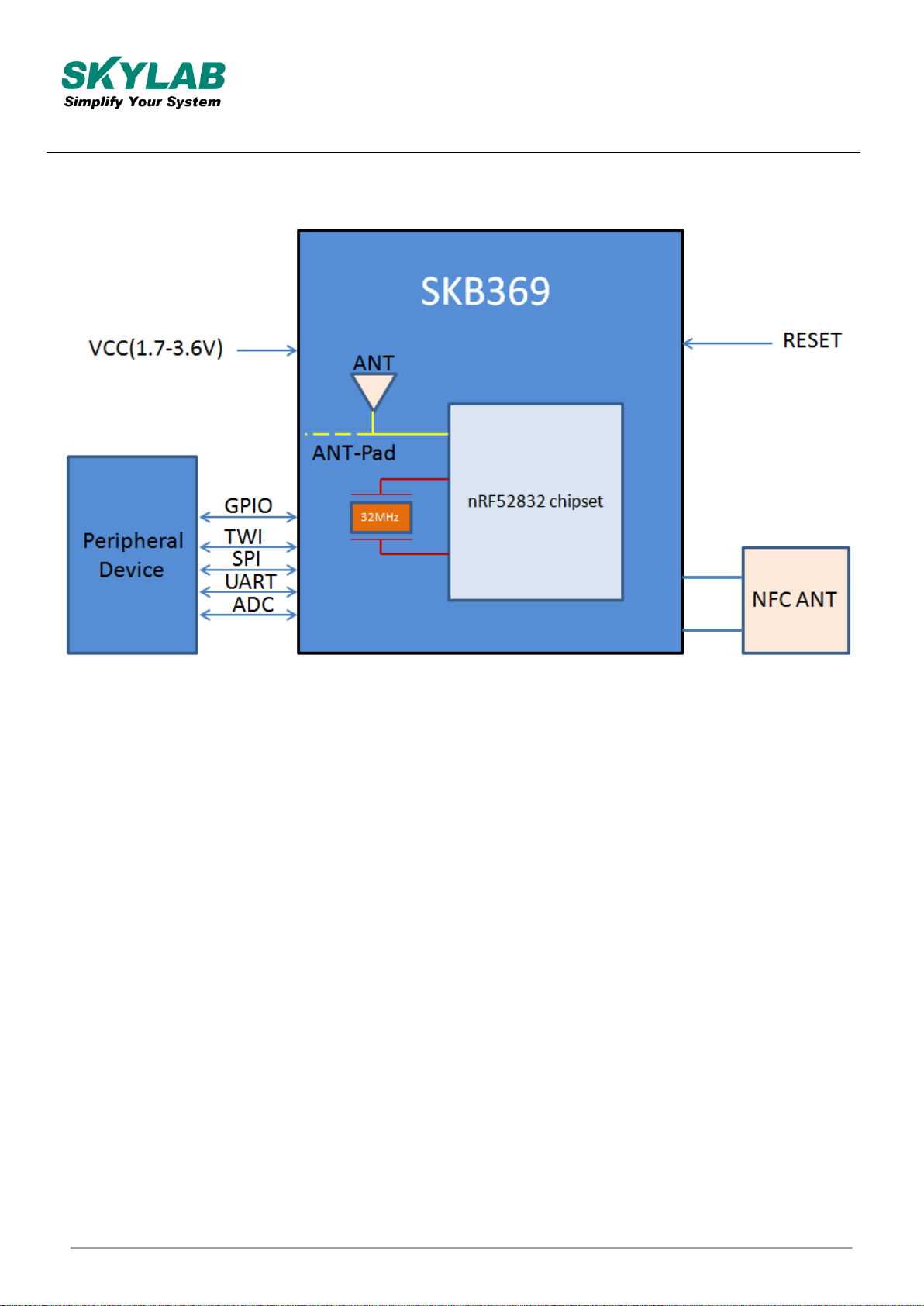
4. Application Block Diagram
Figure 3: SKB369 Block Diagram
SKB369-DA-001,A/1
Page 6

Module SKB369
Bluetooth Module
Skylab M&C Technology Co., Ltd
5. Interfaces
5.1 Power Supply
Regulated power for the SKB369 is required. The input voltage Vcc range should be 1.7V to 3.6V.
Suitable decoupling must be provided by external decoupling circuitry (10uF and 0.1uF). It can reduce
the noise from power supply and increase power stability.
5.2 System Function Interfaces
5.2.1 GPIOs
The general purpose I/O is organized as one port with up to 19 I/Os enabling access and control of up
to 19 pins through one port. Each GPIO can be accessed individually with the following user
configurable features:
1、Input/output direction
2、Output drive strength
3、Internal pull-up and pull-down resistors
4、Wake-up from high or low level triggers on all pins
5、Trigger interrupt on all pins
6、All pins can be used by the PPI task/event system; the maximum number of pins that
can be interfaced through the PPI at the same time is limited by the number of GPIOTE channels
7、All pins can be individually configured to carry serial interface or quadrature demodulator signals
8、All pins can be configured as PWM signal.
9、There are 6 ADC/LPCOMP input in the 19 I/Os.
5.2.2 Two-wire Interface (I2C Compatible)
The two-wire interface can communicate with a bi-directional wired-AND bus with two lines (SCL,
SDA). The protocol makes it possible to interconnect up to 127 individually addressable devices. The
interface is capable of clock stretching, supporting data rates of 100 kbps ,250kbps and 400 kbps. The
module has 2 TWI ports and they properties like following table.
SKB369-DA-001,A/1
Page 7

Module SKB369
Instance
Master/Slave
TWI0
Master
TWI1
Master
Instance
Master/Slave
SPI0
Master
SPI1
Master
SPIS1
Slave
Bluetooth Module
Skylab M&C Technology Co., Ltd
Table5-1: TWI Pin Share Scheme
Note:I2C:Inter-Integrated Circuit
5.2.3 Flash Program I/Os
The module has two programmer pins, respectively SWDCLK pin and SWDIO pin. The two pin Serial
Wire Debug (SWD) interface provided as a part of the Debug Access Port (DAP) offers a flexible and
powerful mechanism for non-intrusive debugging of program code. Breakpoints and single stepping
are part of this support.
5.2.4 Serial Peripheral Interface
The SPI interfaces enable full duplex synchronous communication between devices. They support a
three-wire (SCK, MISO, MOSI) bi-directional bus with fast data transfers. The SPI Master can
communicate with multiple slaves using individual chip select signals for each of the slave devices
attached to a bus. Control of chip select signals is left to the application through use of GPIO signals.
SPI Master has double buffered I/O data. The SPI Slave includes EasyDMA for data transfer directly to
and from RAM allowing Slave data transfers to occur while the CPU is IDLE. The GPIOs are used for
each SPI interface line can be chosen from any GPIOs on the device and configed independently. This
enables great flexibility in device pinout and efficient use of printed circuit board space and signal
routing.
The SPI peripheral support SPI mode 0,1,2,and 3.The module have 3 SPI ports and theirs they
properties are as below:
Table5-2: SPI Properties
SKB369-DA-001,A/1
Page 8

Module SKB369
SKB369 Pin Number
Pin Number
Description
6
P0.28
Digital I/O; Analog input 4
7
P0.29
Digital I/O; Analog input 5
8
P0.30
Digital I/O; Analog input 6
9
P0.31
Digital I/O; Analog input 7
11
P0.02
Digital I/O; Analog input 2
12
P0.03
Digital I/O; Analog input 3
Bluetooth Module
Skylab M&C Technology Co., Ltd
5.2.5 UARTs
The Universal Asynchronous Receiver/Transmitter offers fast, full-duplex, asynchronous serial
communication with built-in flow control (CTS, RTS), support in hardware up to 1 Mbps baud. Parity
checking is supported.
Support the following baudrate in bps unit:
1200/2400/4800/9600/14400/19200/28800/38400/57600/76800/115200.
Note: The GPIOs are used for each SPI/TWI/UART interface line can be chosen from any GPIOs on the device and
configed independently.
5.2.6 Analog to Digital Converter (ADC)
The 12 bit incremental Analog to Digital Converter (ADC) enables sampling of up to 8 external signals
through a front-end multiplexer. The ADC has configurable input and reference prescaling, and
sample resolution (8,10, and 12 bit).
Note: The ADC module uses the same analog inputs as the LPCOMP module. Only one of the modules can be
enabled at the same time.
Table5-3: ADC Pins
5.2.7 Low Power Comparator (LPCOMP)
In System ON, the block can generate separate events on rising and falling edges of a signal, or
sample the current state of the pin as being above or below the threshold. The block can be
configured to use any of the analog inputs on the device. Additionally, the low power comparator can
SKB369-DA-001,A/1
Page 9

Module SKB369
SKB369 Pin Number
Pin Number
Description
16
P0.09
Digital I/O; NFC1
17
P0.10
Digital I/O; NFC2
Bluetooth Module
Skylab M&C Technology Co., Ltd
be used as an analog wakeup source from System OFF or System ON. The comparator threshold can
be programmed to a range of fractions of the supply voltage.
5.2.8 Reset
The reset pin of the SKB369 module is in the internal pull-high state , when the reset pin of the
module is input to a low level , the module will be automatically reset .After the reset pin is used , the
parameters of the current setting will not be ANT .
5.2.9 NFC
The NFC peripheral (referred to as the 'NFC peripheral' from now on) supports communication signal
interface type A and 106 kbps bit rate from the NFC Forum.
With appropriate software, the NFC peripheral can be used to emulate the listening device NFC-A as
specified by the NFC Forum.
Listed here are the main features for the NFC peripheral:
• NFC-A listen mode operation
• 13.56 MHz input frequency
• Bit rate 106 kbps
• Wake-on-field low power field detection (SENSE) mode
• Frame assemble and disassemble for the NFC-A frames specified by the NFC Forum
• Programmable frame timing controller
• Integrated automatic collision resolution, CRC and parity functions
Table5-4: ADC Pins
SKB369-DA-001,A/1
Page 10

Module SKB369
Hardware Features
Model
SKB369
ANTenna Type
PCB ANTenna
Chipset Solution
nRF52832
Voltage
1.7V~3.6V
17.4×13.7×1.9 mm
Bluetooth ® 4.2,ANT
2400MHz---2483.5MHz
1Mbps(Bluetooth ® 4.2)
GFSK Modulation(Bluetooth ® 4.2)
Wireless Security
AES HW Encryption
Transmit Power
Tx Power -20 to +4 dBm in 4 dB Steps(Bluetooth ® 4.2)
Work Mode
Central/Peripheral(Bluetooth ® 4.2)
Others
Certification
RoHS
Environment
Operating Temperature: -40℃~85℃
Storage Temperature: -40℃~125℃
Operating Humidity: 10%~90% Non-condensing
Storage Humidity: 5%~90% Non-condensing
Bluetooth Module
Skylab M&C Technology Co., Ltd
6. Module Specifications
Dimension(L×W×H)
Wireless Features
Wireless Standards
Frequency Range
Data Rates
Modulation
Technique
SKB369-DA-001,A/1
Page 11
Module SKB369
Bluetooth Module
Skylab M&C Technology Co., Ltd
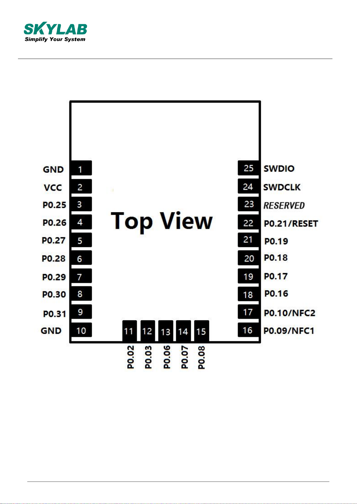
7. Module Pinout and Pin Description
7.1 Module Pinout
Figure 4: SKB369 Module Pinout
SKB369-DA-001,A/1
Page 12

Module SKB369
Pin No.
Pin Name
Description
Remark
1
GND
Ground
2 VCC
Main Power Supply
1.7V to 3.6V
3
P0.25
General Purpose I/O
Digital I/O
4
P0.26
General Purpose I/O
Digital I/O
5
P0.27
General Purpose I/O
Digital I/O
6
P0.28
ADC/LPCOMP input 4
7
P0.29
ADC/LPCOMP input 5
8
P0.30
ADC/LPCOMP input 6
9
P0.31
ADC/LPCOMP input 7
10
GND
11
P0.02
ADC/LPCOMP input 0
12
P0.03
Digital I/O; Analog input
ADC/LPCOMP input 1
13
P0.06
General Purpose I/O
Digital I/O
14
P0.07
General Purpose I/O
Digital I/O
15
P0.08
General Purpose I/O
Digital I/O
16
P0.09/NFC1
Digital I/O;NFC1
Digital I/O;NFC1
17
P0.10/NFC2
Digital I/O;NFC2
Digital I/O;NFC2
18
P0.16
General Purpose I/O
Digital I/O
19
P0.17
General Purpose I/O
Digital I/O
20
P0.18
General Purpose I/O
Digital I/O
21
P0.19
General Purpose I/O
Digital I/O
22
P0.21/RESET
Digital I/O; System Reset
(Active low)
Digital I/O; Reset
23
ANT
24
SWDCLK
Hardware debug and
Flash program I/O
Digital input
25
SWDIO
Digital I/O
Bluetooth Module
Skylab M&C Technology Co., Ltd
7.2 Pin Description
Digital I/O; Analog input
Digital I/O; Analog input
Digital I/O; Analog input
Digital I/O; Analog input
Ground
Digital I/O; Analog input
SKB369-DA-001,A/1
Hardware Debug and
Flash Program I/O
Page 13
Module SKB369
Bluetooth Module
Skylab M&C Technology Co., Ltd
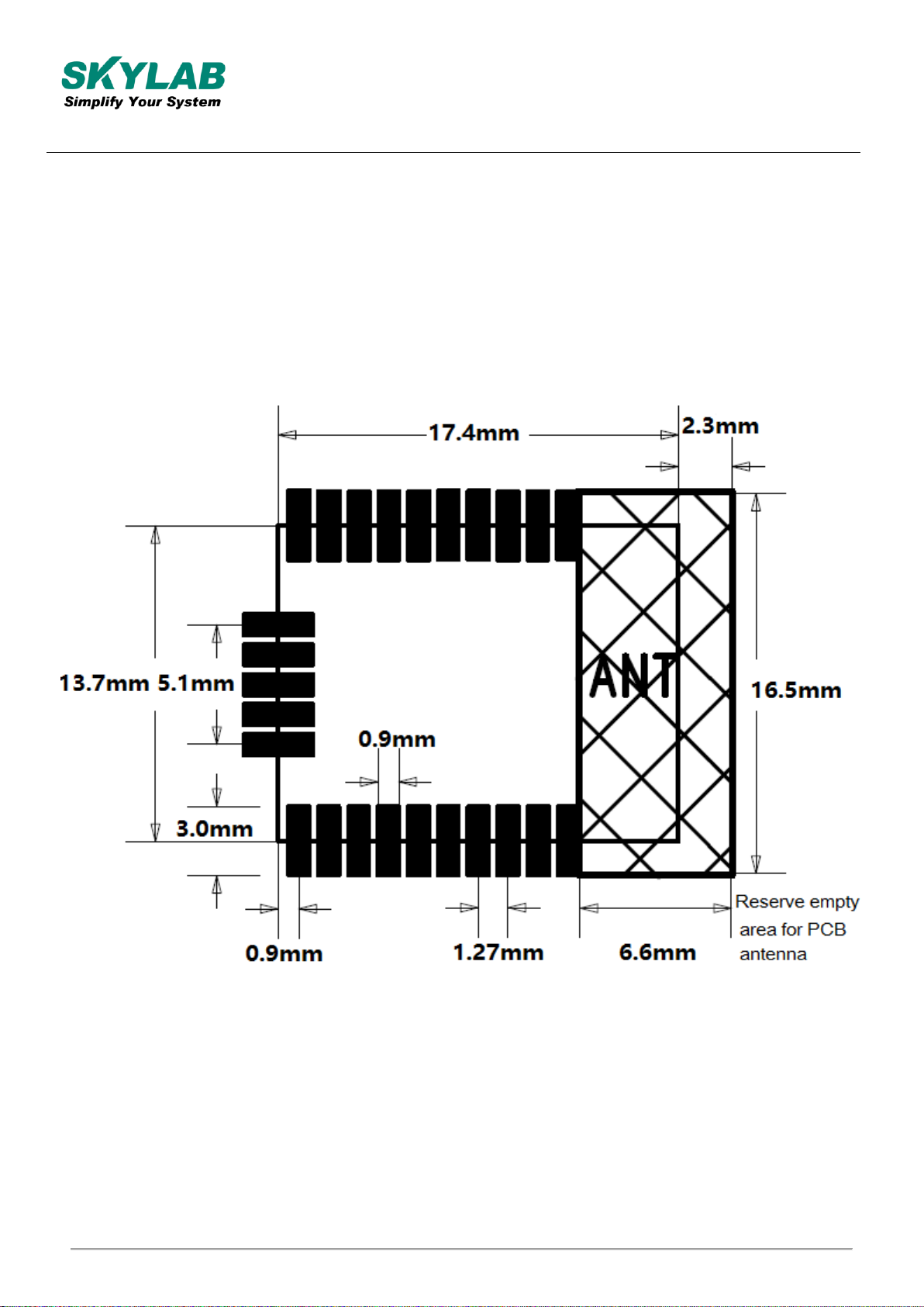
8. PCB Design Guide
Please reserve empty area for PCB ANTenna when you are going to design a device`s
board, the empty range minimum size :
16.5*6.6mm , please kindly check the “PCB footprint and Dimensions” for reference.
9. PCB Footprint and Dimensions
Figure 5: SKB369 Recommended PCB Footprint
SKB369-DA-001,A/1
Page 14
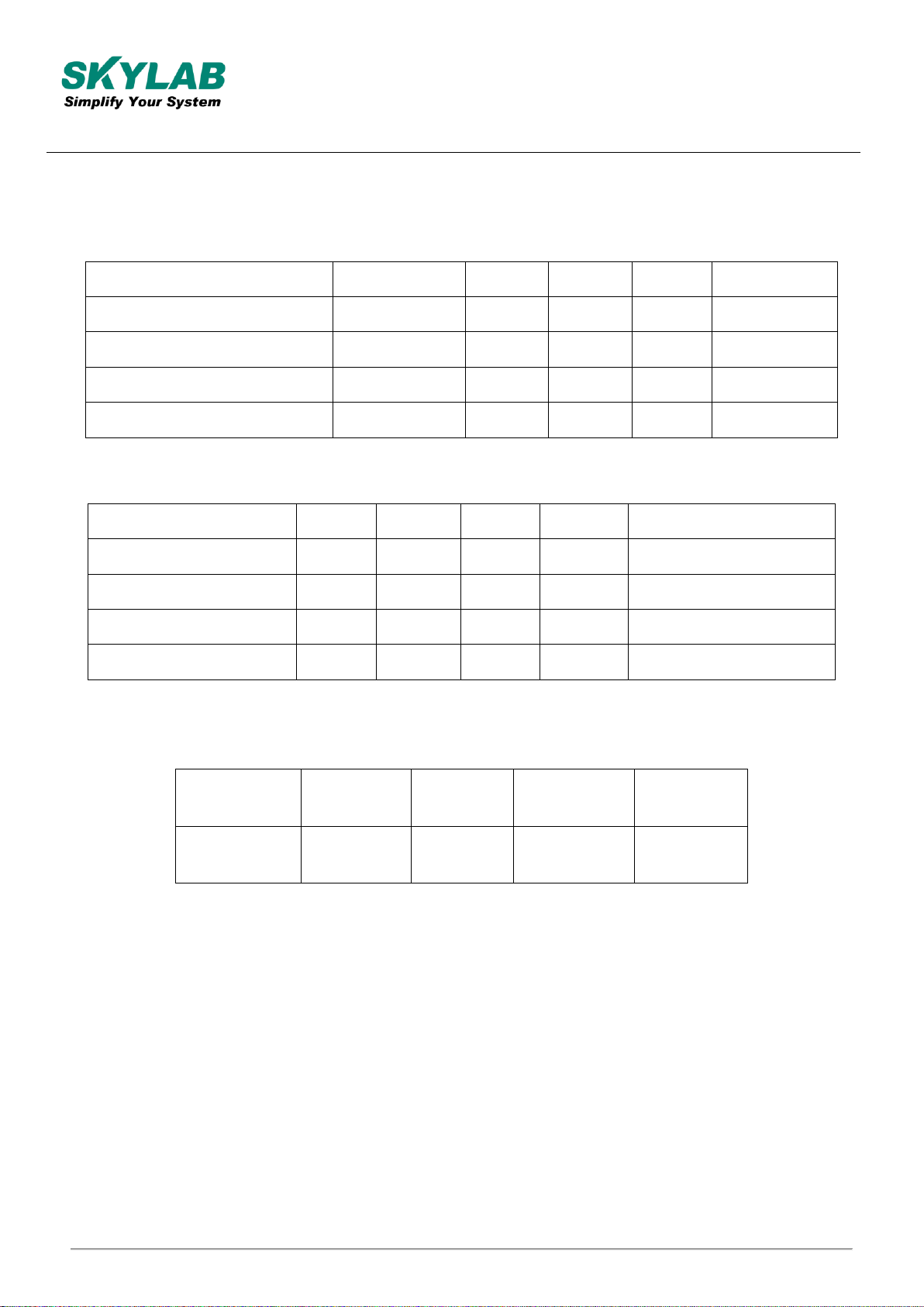
Module SKB369
Parameter
Condition
Min.
Typ.
Max.
Unit
Storage Temperature Range
-40
125
°C
ESD Protection
VESD
/
4000
V
Supply Voltage
VCC
-0.3
3.9
V
-0.3
3.63
V
Max.
Unit
85
ºC
3.6
V
0.3*VCC
V
Input High Voltage
VIH
0.7*VCC
VCC
V
System State
TX Peak
@4dBm
RX Peak
Sleep Mode
(avg)
Idle Mode
(avg)
Current
(peak)@3V
7.5 mA
5.4 mA
0.4uA
1.2uA
Bluetooth Module
Skylab M&C Technology Co., Ltd
10. Electrical Characteristics
10.1 Absolute Maximum Ratings
Voltage On Any I/O Pin
Table10-1: Absolute Maximum Ratings
10.2 Recommended Operation Ratings
Parameter Symbol Min. Typ.
Extended Temp. Range TA -40 25
Power Supply VCC 1.7 3.3
Input Low Voltage VIL 0
Table10-2: Operating Conditions
10.3 Current
Table10-3: Power Consumption in Different States
SKB369-DA-001,A/1
Page 15
Module SKB369
Bluetooth Module
Skylab M&C Technology Co., Ltd
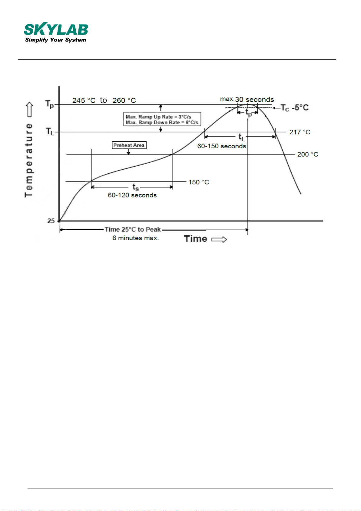
11. Manufacturing Process Recommendations
Figure 6: SKB369 Typical Lead-free Soldering Profile
Note:The final re-flow soldering temperature map chosen at the factory depends on additional external factors, for
example, choice of soldering paste,size, thickness and properties of the module`s baseboard etc. Exceeding the
maximum soldering temperature in the recommended soldering profile may permanently damage the module.
SKB369-DA-001,A/1
Page 16
Module SKB369
Module No.
Crystal
Shielding
ANTenna
Temperature Grade
SKB369-CSPI
32.768K
Shielding
PCB
Industry
SKB369-XXPI
No
No
PCB
Industry
Bluetooth Module
Skylab M&C Technology Co., Ltd
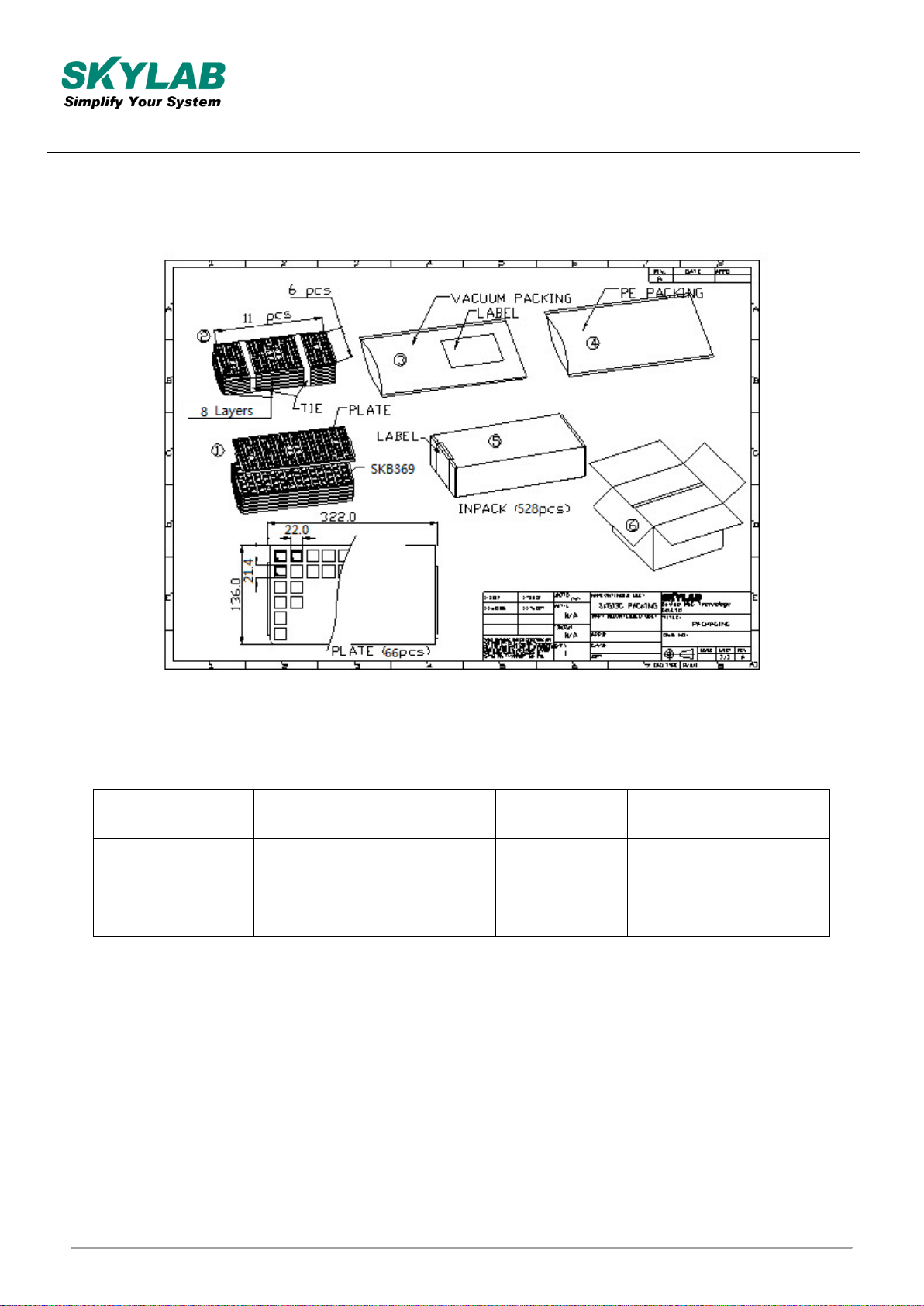
12. Packaging Specification
SKB369 modules are put into tray and 528 units per tray. Each tray is ‘dry’ and vacuum packaging.
13. Ordering Information
Figure 7: SKB369 Packaging
16 / 17 SKB369-DA-001,A/1
Page 17
Skylab M&C Technology Co., Ltd
Module SKB369
Bluetooth Module
SKB369-DA-001,A/1
Page 18

Module SKB369
Bluetooth Module
Skylab M&C Technology Co., Ltd
FCC Radiation Exposure Statement
The modular can be installed or integrated in mobile or fix devices only. This modular
be installed in any portable device, for example, USB dongle like transmitters is forbidden.
This modular complies with FCC RF radiation exposure limits set forth for an uncontrolled
environment. This transmitter must not be collocated or operating in conjunction with
antenna or transmitter.
If the FCC identification number is not visible when the module is installed inside another
device, then the outside of the device into which the module is installed must also display
label referring to the enclosed module.
This exterior label can use wording such as the following:
“Contains Transmitter Module FCC ID:2ACOE-SKB369 Or Contains FCC ID:2ACOE-SKB369
when the module is installed inside another device, the user manual of this device must
contain below warning statements;
1. This device complies with Part 15 of the FCC Rules. Operation is subject to the following
two conditions:
(1) This device may not cause harmful interference.
(2) This device must accept any interference received, including interference that may
undesired operation.
2. Changes or modifications not expressly approved by the party responsible for compliance
could void the user's authority to operate the equipment.
The devices must be installed and used in strict accordance with the manufacturer's
instructions as described in the user documentation that comes with the product.
This device is intended only for OEM integrators under the following
1) The antenna must be installed such that 20 cm is maintained between the antenna
and user.
2) The transmitter module may not be coÿlocated with any other transmitter or
antenna.
Module Antenna Type: PCB ANT, 1dBi gain
conditions:
15. Contact Information
Skylab M&C Technology Co., Ltd.
深圳市天工测控技术有限公司
Address: 6 Floor, No.9 Building, Lijincheng Scientific & Technical park, Gongye East Road,
Longhua District, Shenzhen, Guangdong, China
Phone: 86-755 8340 8210(Sales Support)
Phone: 86-755 8340 8510(Technical Support)
Fax: 86-755-8340 8560
E-Mail: [email protected]
Website: www.skylab.com.cn www.skylabmodule.com
SKB369-DA-001,A/1
 Loading...