

SiRF SiRFatlasV Design Manual

Design Guide
SiRF Proprietary and Confidential
SiRFatlasV
Audio Hardware Design Guide
January 2010
Document Number: CS-130255-UG
Issue 2
INTRODUCTION
This document serves as a hardware design guide for SiRFatlasVTM audio, including the input and output
paths.

SiRFatlasV
Audio Hardware Design Guide
January, 2010 SiRF Design Guide – Proprietary and Confidential 2
Table of Contents
Introduction ................................................................................................................... 1
Audio Output Path......................................................................................................... 3
Audio Output Path......................................................................................................... 3
DigDAC Overview ......................................................................................................................... 3
Application Information.................................................................................................................. 4
Speaker.............................................................................................................................. 4
Headphone......................................................................................................................... 6
Audio Input Path............................................................................................................ 8
Pre-amplifier .................................................................................................................................8
SAR ADC......................................................................................................................................8
Application Information.................................................................................................................. 9
Setting the AGC Threshold (R5 and R7) .............................................................................9
Input Capacitor (C4) ...........................................................................................................9
Power Supply ..................................................................................................................... 9
RC Buffer .........................................................................................................................10
PCB Layout ...................................................................................................................... 10
Performance and Measurement ..................................................................................................10
Terminology................................................................................................................. 11
List of Figures
Figure 1: DigDAC Block Diagram.............................................................................................................3
Figure 2: Speaker Circuit .........................................................................................................................4
Figure 3: Frequency Response of RC Filter .............................................................................................5
Figure 4: Headphone Circuit .................................................................................................................... 6
Figure 5: Frequency Response of Headphone RC Filter ..........................................................................7
Figure 6: Input Audio Chain .....................................................................................................................8
Figure 7: Pre-amplifier Circuit ..................................................................................................................9
Figure 8: A-weighted Filter Frequency Response...................................................................................11
SiRFatlasV
Audio Hardware Design Guide
January, 2010 SiRF Design Guide – Proprietary and Confidential 3
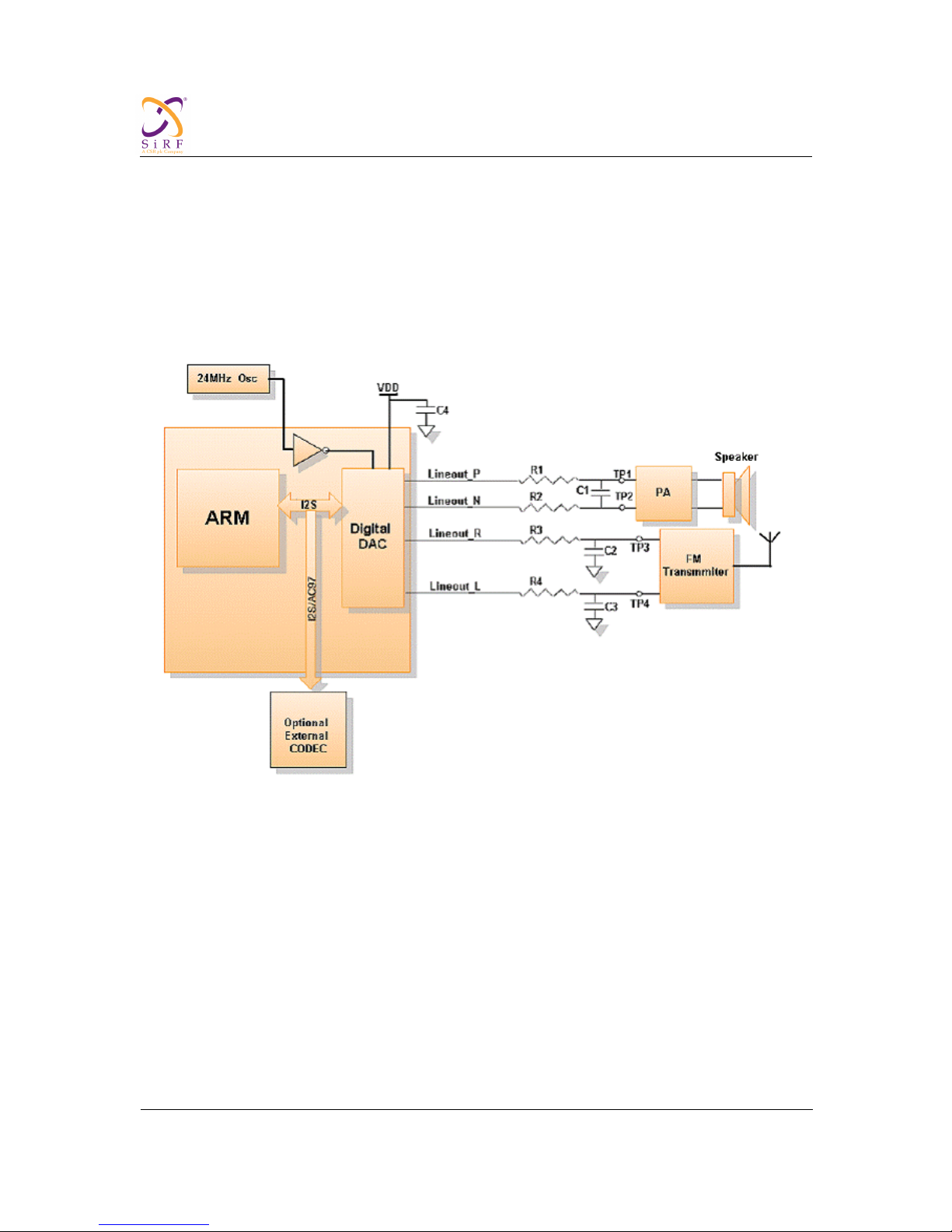
AUDIO OUTPUT PATH
The SiRFatlasV audio output path is built using pure digital IP DigDAC.
DigDAC Overview
DigDAC is a digital Virtual Component. The DigDAC architecture uses an entirely digital approach to
convert digital source input to a PWM signal output. This virtual component features a flexible clock
management system in order to eliminate external audio PLL requirements. It is also optimized for
operation with external amplifiers (analog line out), requiring low out-of-band energy emissions.
Figure 1: DigDAC Block Diagram
SiRFatlasV
Audio Hardware Design Guide
January, 2010 SiRF Design Guide – Proprietary and Confidential 4
Application Information
Speaker
Performance
SNR = 81dB
THD = 75dB (0.017%)
Output voltage full-scale swing (differential) = 970mV rms
NOTE - The performance has been tested after the RC filter. The test points are TP1 and TP2 as
illustrated in Figure 1.
Test Condition:
Test equipment: Audio precision ATS-2
ATS-2 setting: A-weighted filter; 10Hz~20kHz low-pass filter
DigDAC setting: Volume = 0dB (0x79h)
When testing the SNR, set the input signal to 0 to get the noise floor of the headphone output.
Sample rate: 48K/s
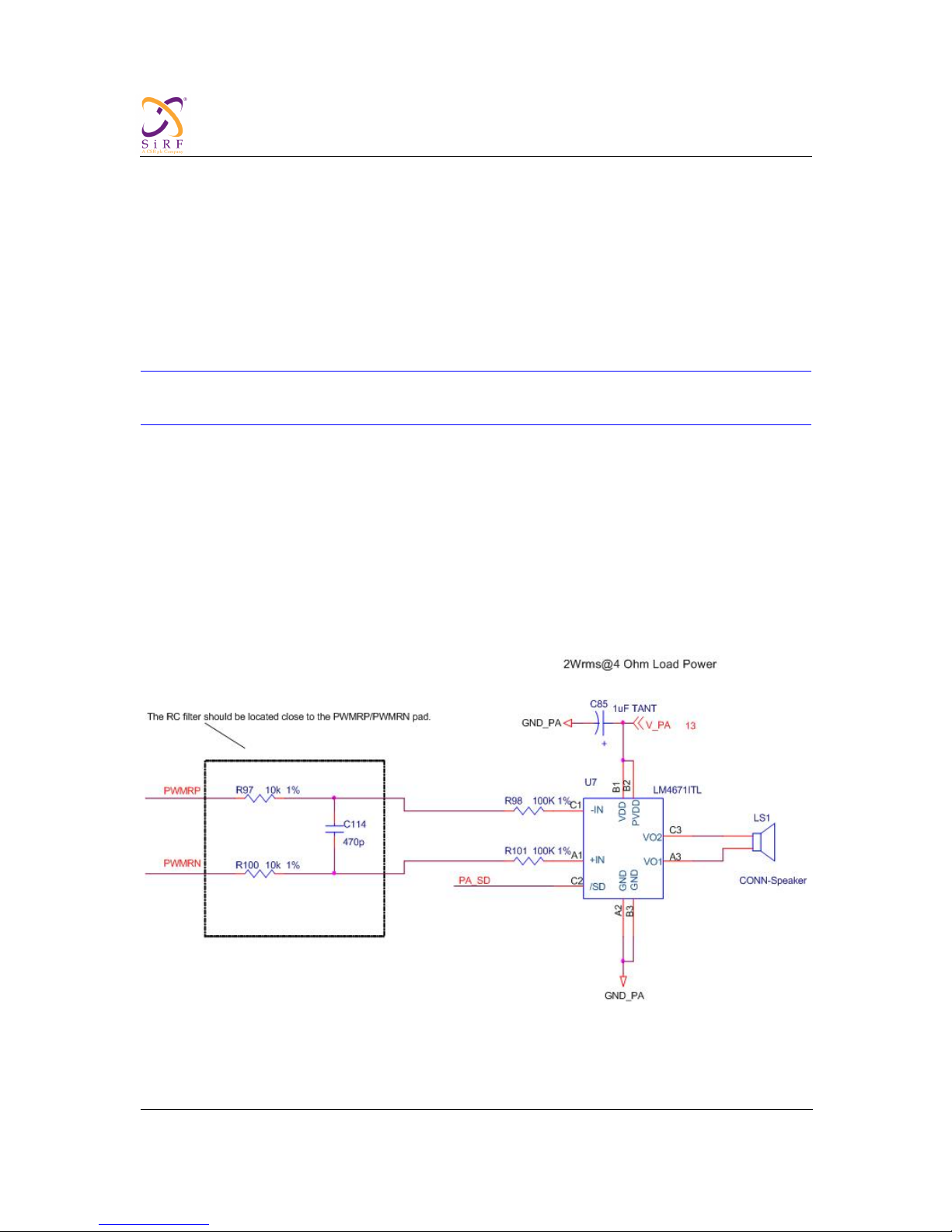
Speaker Circuit Design
Figure 2: Speaker Circuit
 Loading...