

Page 1
Solved by
TM
Easy Evaluation of the SP7662ER
0 to 12A Output Synchronous Buck
Converter
Built in Low R
UVLO Detects Both VCC and VIN
Highly Integrated Design, Minimal
Components
High Efficiency: up to 93%
Feature Rich: UVIN, Programmable
Soft Start, Built In VCC Supply
Output Short Circuit Protection and
Current Limiting
DS(ON) Power FETs
SP7662
Evaluation Board Manual
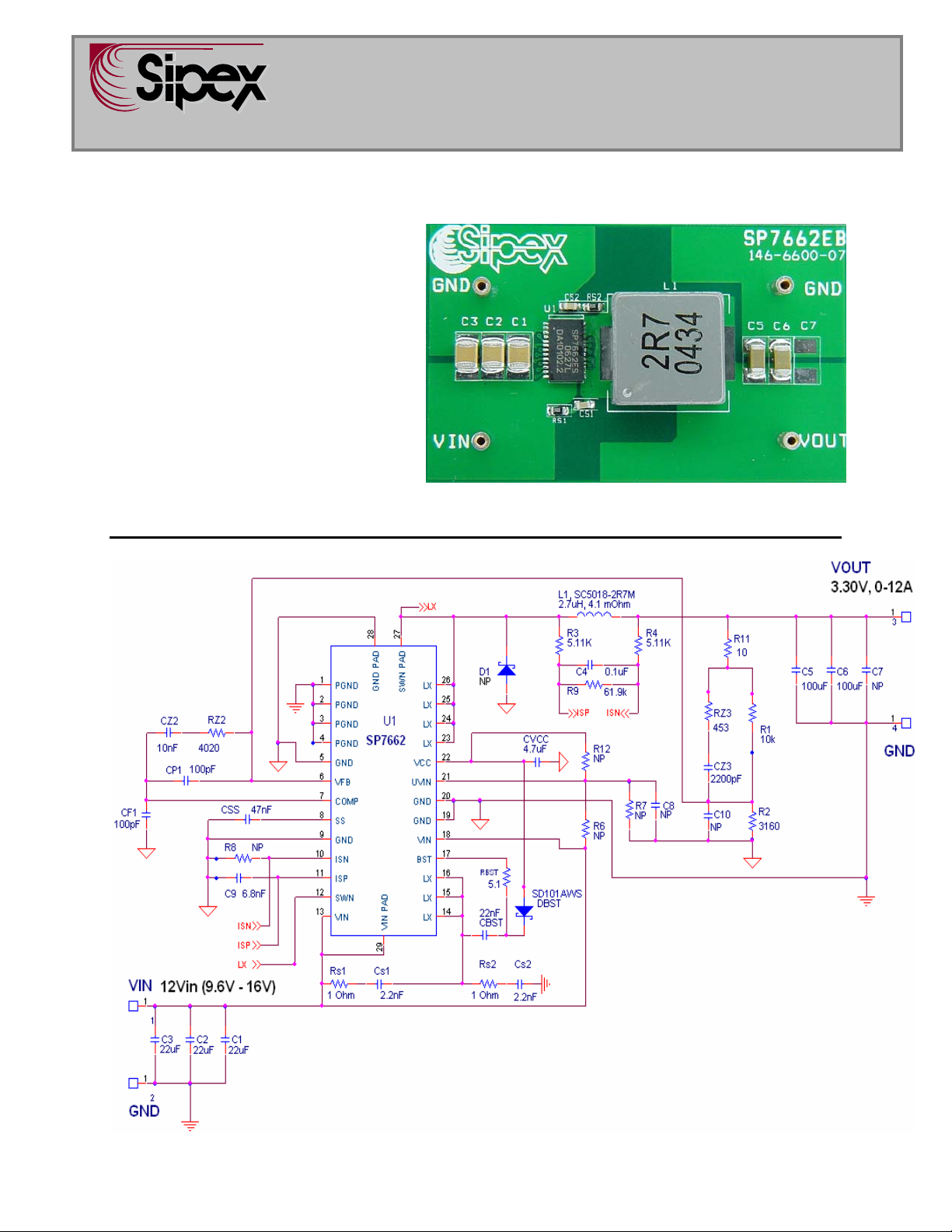
SP7662EB Schematic
Nov27-06 SP7662 Evaluation Board Manual © 2006 Sipex Corporation
Page 2

+
⋅
Using the Evaluation Board
1) Powering Up the SP7662EB Circuit
Connect the SP7662 Evaluation Board with an external +12V power supply. Connect with short
leads and large diameter wire directly to the “VIN” and “GND” posts. Connect a Load between
the VOUT and GND posts, again using short leads with large diameter wire to minimize
inductance and voltage drops.
beyond 10 Amps for extended periods.
2) Measuring Output Load Characteristics
VOUT ripple can best be seen by touching the probe tip to the pad for C5 and the scope GND
collar touching the Output GND post – avoid a GND lead on the scope which will increase noise
pickup.
3) Using the Evaluation Board with Different Output Voltages
While the SP7662 Evaluation Board has been tested and delivered with the output set to 3.30V,
by simply changing one resistor, R2, the SP7662 can be set to other output voltages. The
relationship in Equation 1 is based on a voltage divider from the output to the feedback pin V
which is set to an internal reference voltage of 0.80V. Note, due to the common mode voltage
range of the current sense amplifier, output voltages greater than 3.3V are only possible if the
current sense is disabled. To disable current limit, remove R3 and R4. Standard 1% metal film
resistors of surface mount size 0603 are recommended.
Where R1 = 10kΩ and for V
Furthermore, one could select the value of the R1 and R2 combination to meet the exact output
voltage setting by restricting R1 resistance range such that 10KΩ ≤ R1 ≤ 100KΩ for overall
system loop stability.
Note that since the SP7662 Evaluation Board design was optimized for 12V down conversion to
3.30V, changes of output voltage and/or input voltage will alter performance from the data given
in the Power Supply Data section. In addition, the SP7662ER provides short circuit protection by
sensing V
OUT at GND. The current limit of the converter is set to about 17A which is
accomplished by sensing the current through the inductor. To adjust the current limit, follow
Equations 2 and 3 to set the current limit accordingly. The current limit should be set to about
50% higher than the maximum output current that is desired. This will prevent the part from
accidentally triggering the current limit during large transient load steps.
Adjusting the Current upward is done by adjusting resistor R9.
R9
Where DCR is the Inductor winding resistance
I
Provide >=100lfm of airflow if powering the evaluation board
R2
OUT = 0.80V setting, simply remove R2 from the board.
Vout
.80V
R1
=
I
⋅
MAX is the desired output current
Equation 1
−=1
R4)R3(60mV
60mV)-DCR(max
Equation 2
FB,
Feb21-07 SP7662 Evaluation Manual ©2007 Sipex Corporation
Page 2 of 11
Page 3
Adjusting the Current downward is controlled by adjusting R8.
⋅=
R4R8
⋅+
DCR)(Imax60mV)-(Vout
⋅
DCR)(Imax-60mV
Where DCR is the Inductor winding resistance
I
MAX is the desired output current
Further details on the current limit can be found in the SP7662 data sheet.
For the Inter-Technical Inductor on this demo board DCR= 4.1mΩ nominal.
POWER SUPPLY DATA
The SP7662ER is designed with an very accurate 2.0% reference over line, load and
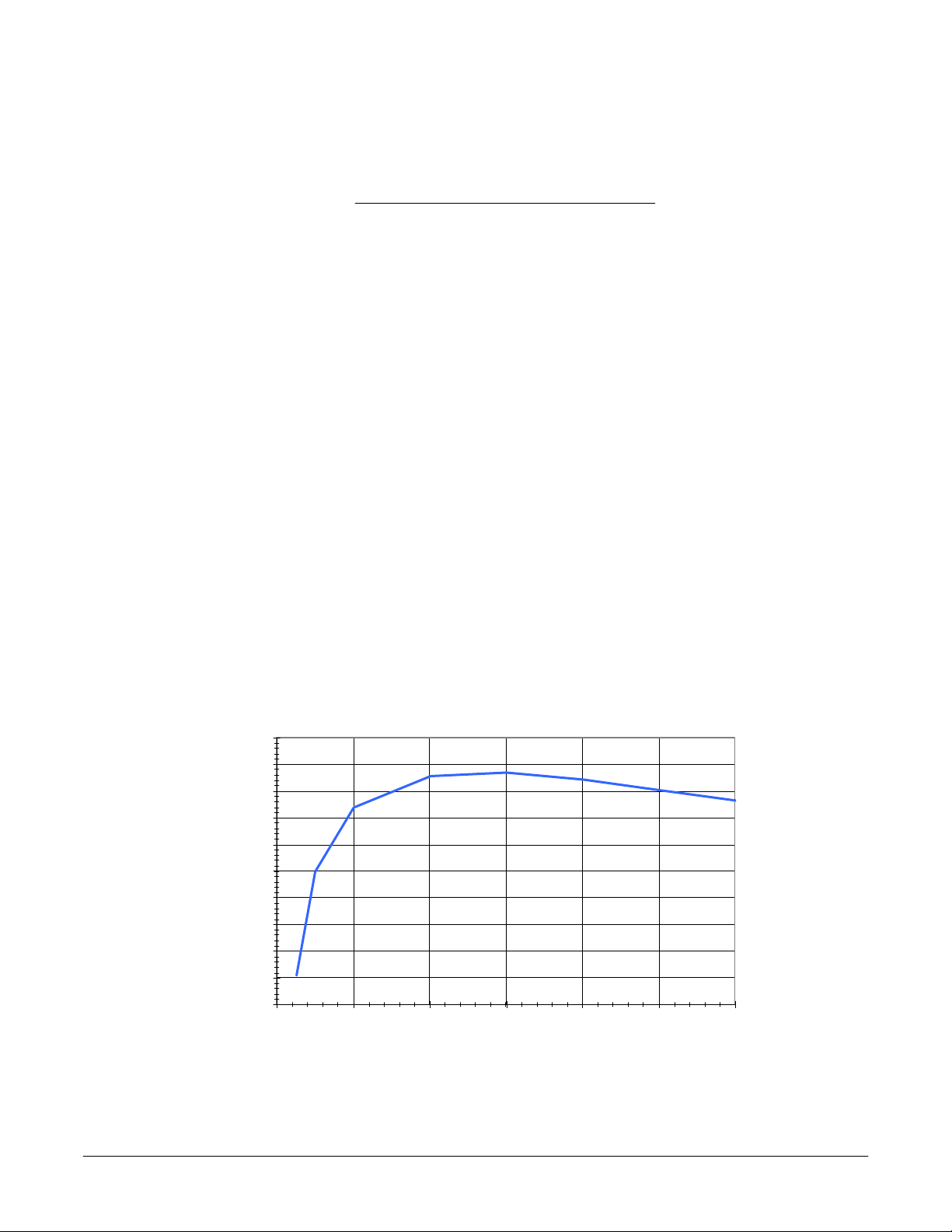
temperature. Figure 1 data shows a typical SP7662 evaluation board efficiency plot, with
efficiencies up to 93% and output currents up to 12A. The output voltage ripple of less than
30mV at full load and the LX node are shown in figure 2. Figures 3 and 4 illustrate a 6A-to-12A
and 0A-to-12A Load Step. Short circuit and current limit are shown in Figures 5 and 6. Typical
startup characteristics into a full load and no load are shown in figures 7 and 8. All data was
taken at 12V
IN.
While data on individual power supply boards may vary, the capability of the SP7662ER
of achieving high accuracy over a range of load conditions shown here is quite impressive and
desirable for accurate power supply design.
Equation 3
7662 Efficiency
12Vin - 3.3Vout - 12Amps
96.00
94.00
92.00
90.00
88.00
86.00
84.00
Efficiency
82.00
80.00
78.00
76.00
024681012
Iout (Amps)
Figure 1. Efficiency vs Load
Feb21-07 SP7662 Evaluation Manual ©2007 Sipex Corporation
Page 3 of 11
Page 4
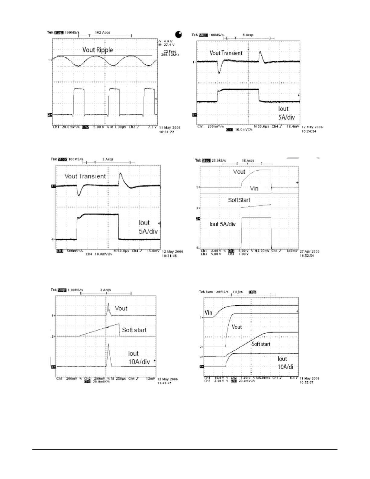
Figure 2. LX node output ripple voltage Figure 3. Load Step Response: 6->12A
Figure 4. Load Step Response 0->12A Figure 5. Current limit set point 17A
Figure 6. Output load Short Circuit Figure 7. Startup into full load
Feb21-07 SP7662 Evaluation Manual ©2007 Sipex Corporation
Page 4 of 11
Page 5
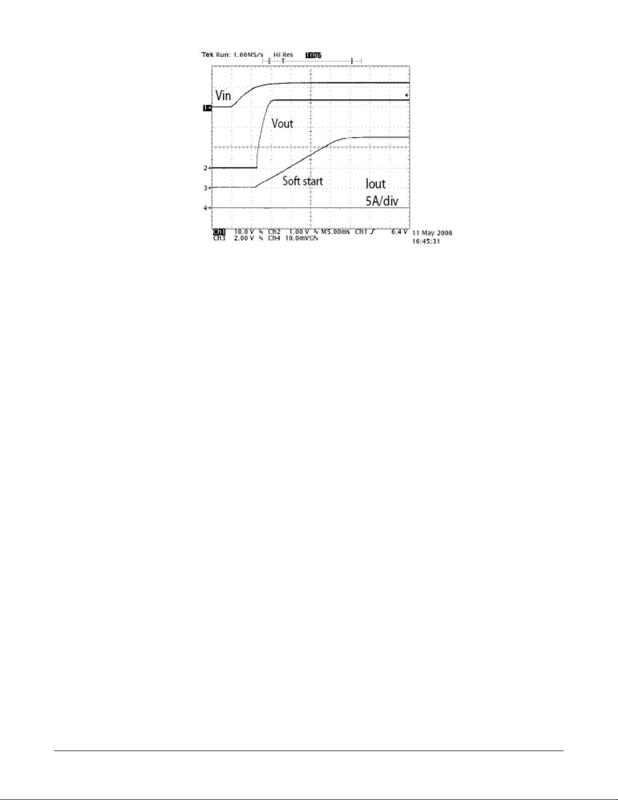
Figure 8. Startup into no load
TYPE III LOOP COMPENSATION DESIGN
The open loop gain of the SP7662EB can be divided into the gain of the error amplifier
Gamp(s), PWM modulator Gpwm, buck converter output stage Gout(s), and feedback resistor
divider Gfbk. In order to cross over at the selecting frequency fco, the gain of the error amplifier
must compensate for the attenuation caused by the rest of the loop at this frequency. The goal
of loop compensation is to manipulate the open loop frequency response such that its gain
crosses over 0dB at a slope of –20dB/dec. The open loop crossover frequency should be higher
than the ESR zero of the output capacitors but less than 1/5 to 1/10 of the switching frequency
fs to insure proper operation. Since the SP7662EB is designed with Ceramic Type output
capacitors, a Type III compensation circuit is required to give a phase boost of 180° in order to
counteract the effects of the output LC underdamped resonance double pole frequency.
Feb21-07 SP7662 Evaluation Manual ©2007 Sipex Corporation
Page 5 of 11
Page 6
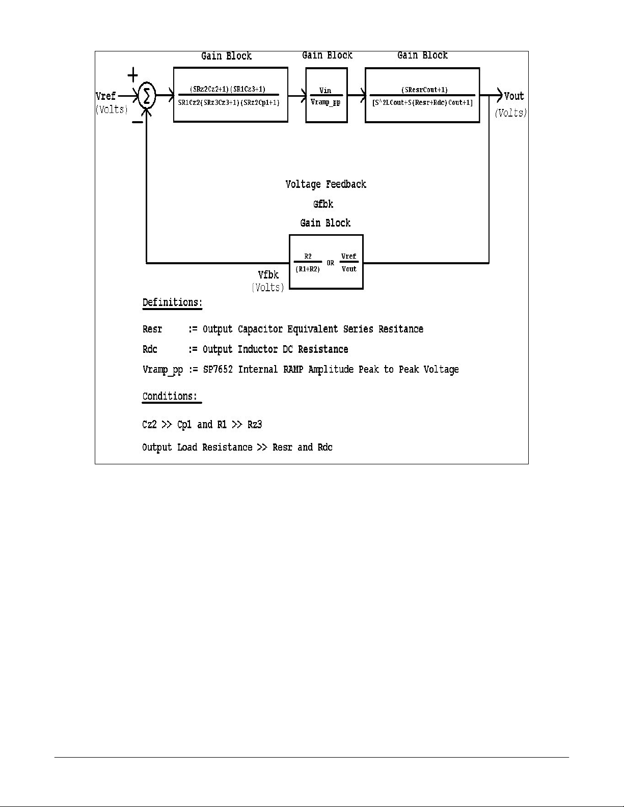
Figure 9. Voltage Mode Control Loop with Loop Dynamic for Type III Compensation
The simple guidelines for positioning the poles and zeros and for calculating the
component values for Type III compensation are as follows. As a particular example, consider
for the following SP7662EB with a Type III Voltage Loop Compensation component selections:
Input requirements and inductor selection
V
IN = 12V, we will use 12V as VIN max for this design
V
OUT = 3.30V @ 0 to 12A load
Select L = 2.7uH => yield ≈ 25% of maximum 12A output current ripple
Select C
OUT = 100uF Ceramic capacitor (RESR ≈ 3mΩ)
fs = 300kHz SP7662 internal Oscillator Frequency
V
RAMP_PP = 1.0V SP7662 internal Ramp Peak-to-Peak Amplitude
Feb21-07 SP7662 Evaluation Manual ©2007 Sipex Corporation
Page 6 of 11
Page 7
=
Step by step design procedures
Choose
Calculate fp_LC the double pole frequency of the filter
Note: Loop Compensation component calculations discussed
in this section can be quickly iterated with the Type III Loop
Compensation Calculator on the web at:
www.sipex.com/files/Application-Notes/TypeIIICalculator.xls
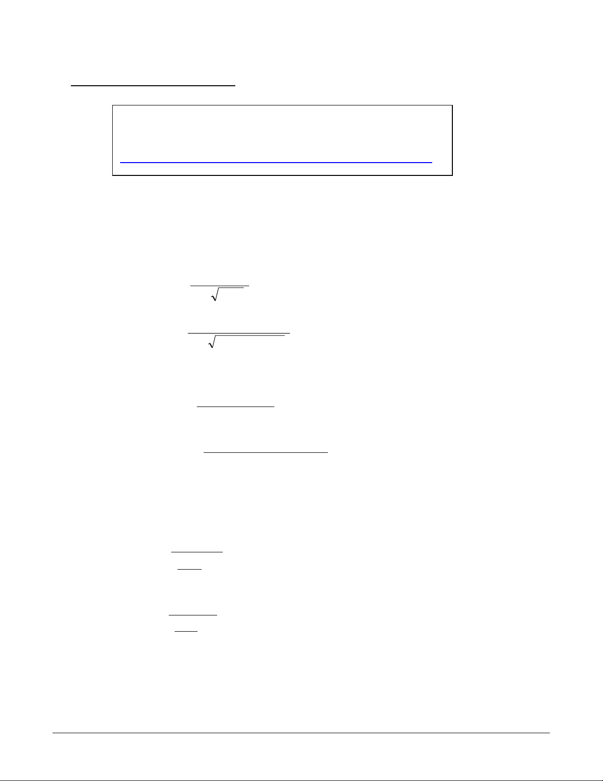
fs/10fco =
=
:
30kHz300kHz/10fco
1
fp_LC⋅=
π
Calculate fz_ESR the ESR zero frequency
fp_LC ≈=
=
)CL(2
1
⋅⋅
)200uF2.7uH2π
1
fz_ESR
=
⋅⋅
CoutCesr2π
1
_ =
Select R1 component value such that 10kΩ ≤ R1 ≤ 100kΩ
R1 = 10kΩ, 1%
Calculate R2 based on the desired V
=
R
2
= 31603200
2
R
=
ESRfz 530
Vout
⋅⋅
OUT
R
1
1
−
V
8.
Ω
1.68
K
3.3
V
−
1
8.
V
µFmΩπ
)200()2/3(2
Ω≈Ω=
7kHz6852hz
kHz
Feb21-07 SP7662 Evaluation Manual ©2007 Sipex Corporation
Page 7 of 11
Page 8

Select the ratio of RZ2 / R1 gain for the desired gain bandwidth (we will use slightly higher than
30kHz @ 33kHz)
⋅=
RRZ
12
Calculate CZ2 by placing the zero at ½ of the output filter pole frequency
CZ
2⋅⋅=
⋅= 40203928
12
RRZ
12
Vin
1
V
_
⋅
V
1
π
33
7
ppVramp
_2
kHz
kHz
LCfpRZ
⋅
fco
_max_
LCfp
Ω≅Ω=
1
2 ≈=
=
CZ 1011
π
Calculate CP1 by placing the first pole at ESR zero frequency
1
=
π
CP 100133
1 ≈=
=
π
Calculate RZ3 by setting the second pole at ½ of the switching frequency and the second zero
at the output filter double pole frequency
RZ
3
=
RZ
3
= 453489
Calculate CZ3 from RZ3 component value above
3
1
π
⋅Ω⋅
kHz
74020
1
1
⋅⋅
⋅⋅
−
⋅Ω⋅
⋅−
ESRfzRzCP⋅⋅
KHz
_2
kHzk
kHzKHz
72300
)_2(2
)5304020(2
LCfpR
)_()1(2
LCfpfs
)7()10(2
fsRZCZ⋅⋅=3
nFnF
pFpF
Ω≅Ω=
1
CZ 22003.2
3 ≈=
=
π
Choose 100pF ≤ CF1 ≤ 220pF to stabilize the SP7662ER internal Error Amplifier . For this
example let’s select 100pF.
KHz
300453
⋅Ω⋅
pFnF
Feb21-07 SP7662 Evaluation Manual ©2007 Sipex Corporation
Page 8 of 11
Page 9
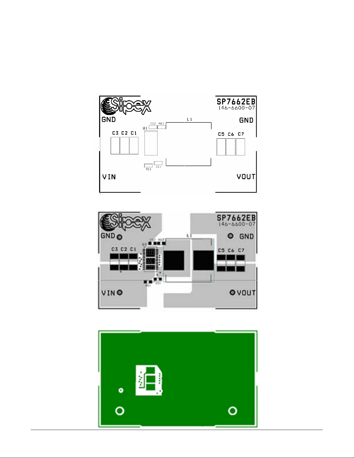
PC Layout Drawings
Figure 15. SP7662EB Component Placement
Figure 16. SP7662EB PC Layout Top Side
Feb21-07 SP7662 Evaluation Manual ©2007 Sipex Corporation
Page 9 of 11
Page 10
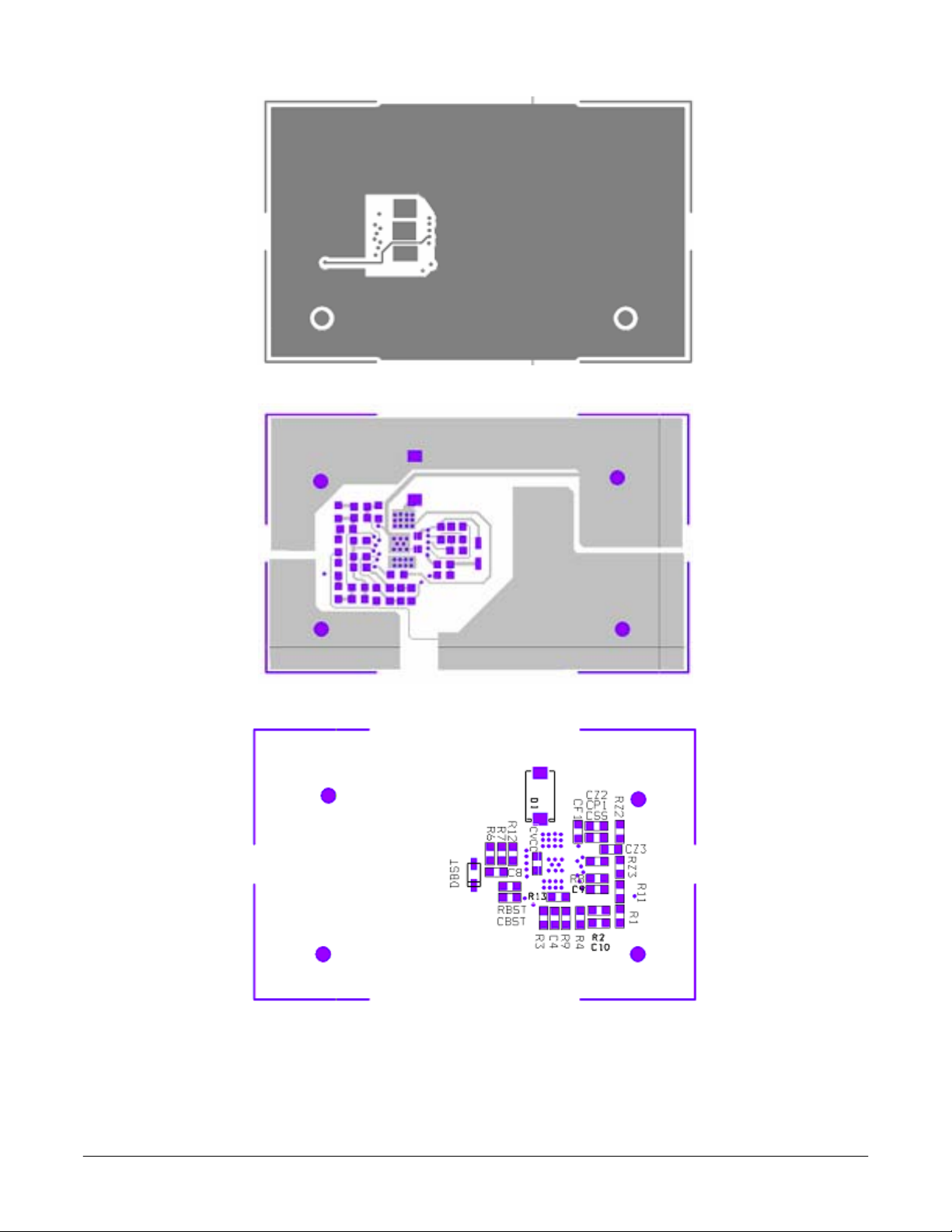
Figure 17. SP7662EB PC Layout 2nd Layer Side
Figure 18. SP7662EB PC Layout 3
rd
Layer Side
Figure 19. SP7662EB PC Layout Bottom Side
Figure 20. SP7662EB PC Layout Bottom Side Components
Feb21-07 SP7662 Evaluation Manual ©2007 Sipex Corporation
Page 10 of 11
Page 11
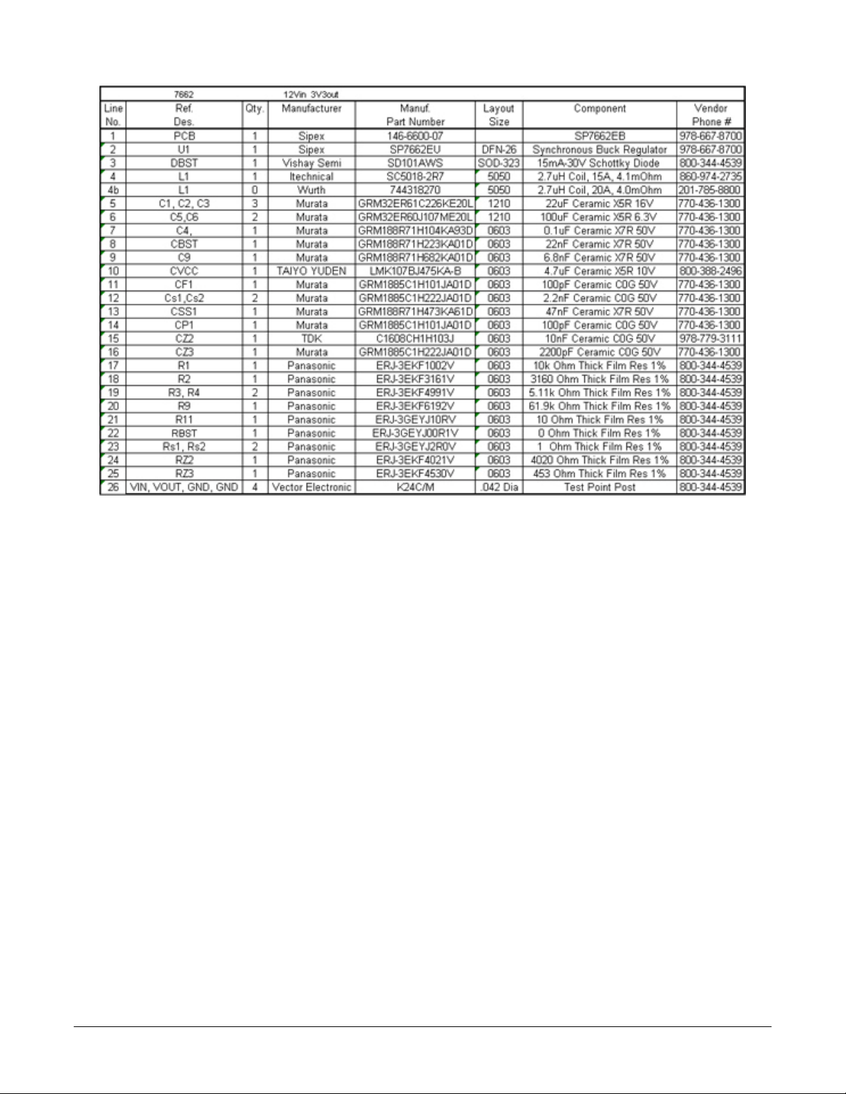
Table 1: SP7662EB Suggested Components and Vendor Lists
ORDERING INFORMATION
Model Temperature Range Package Type
SP7662EB…................................-40°C to +85°C...............…………….SP7662 Evaluation Board
SP7662ER..............................…. -40°C to +85°C...................................……26-pin DFN(option2)
Feb21-07 SP7662 Evaluation Manual ©2007 Sipex Corporation
Page 11 of 11
 Loading...