

Page 1
Easy Evaluation for the
SP7650ER 12V Input, 0 to 3A
Output Synchronous Buck
Converter
Built in Low Rds(on) Power FETs
UVLO Detects Both VCC and VIN
High Integrated Design, Minimal
Components
High Efficiency: 90%
Feature Rich: UVIN, Programmable
Softstart, External VCC Supply and
Output Dead Short Circuit Shutdown
SP7650
Evaluation Board Manual
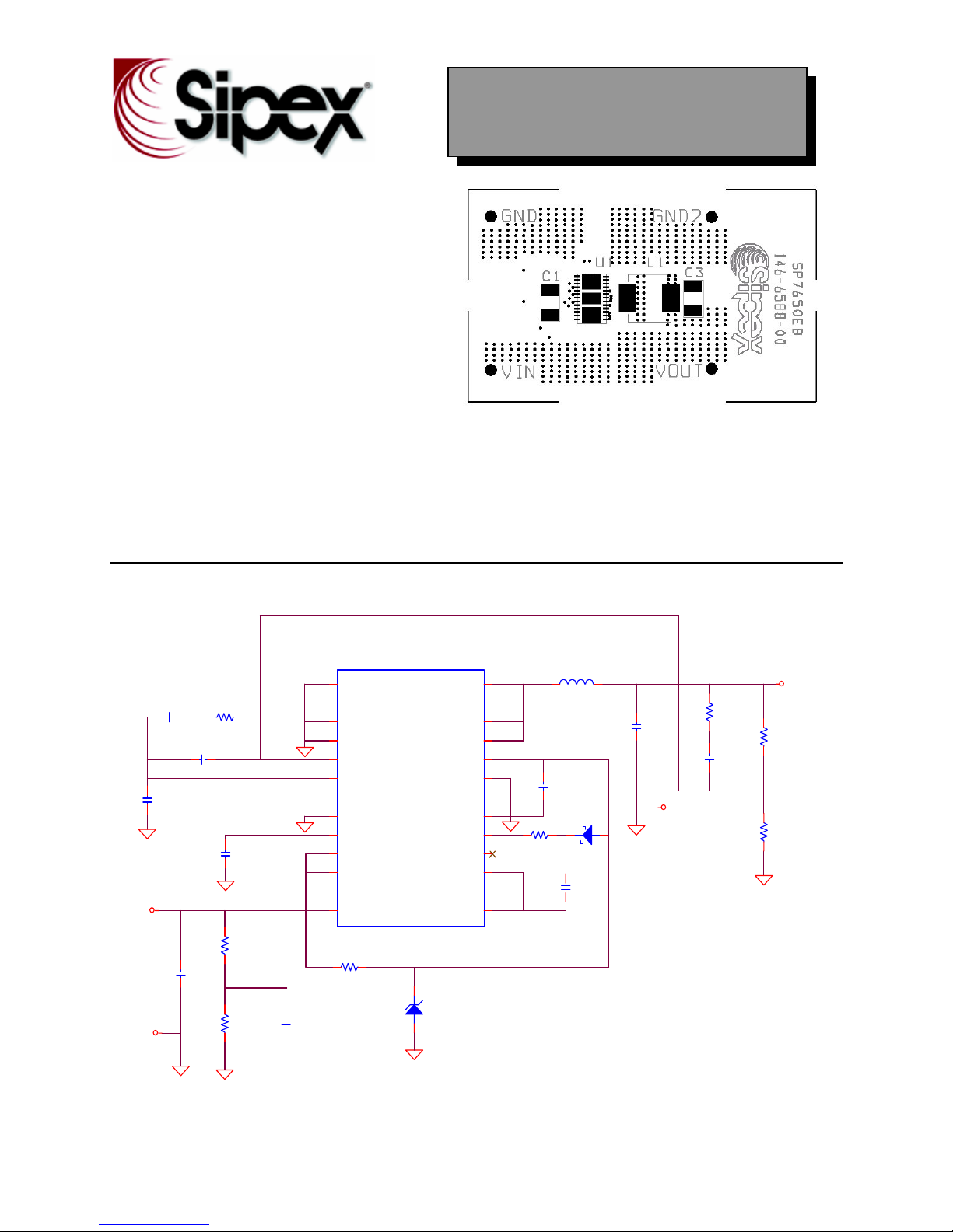
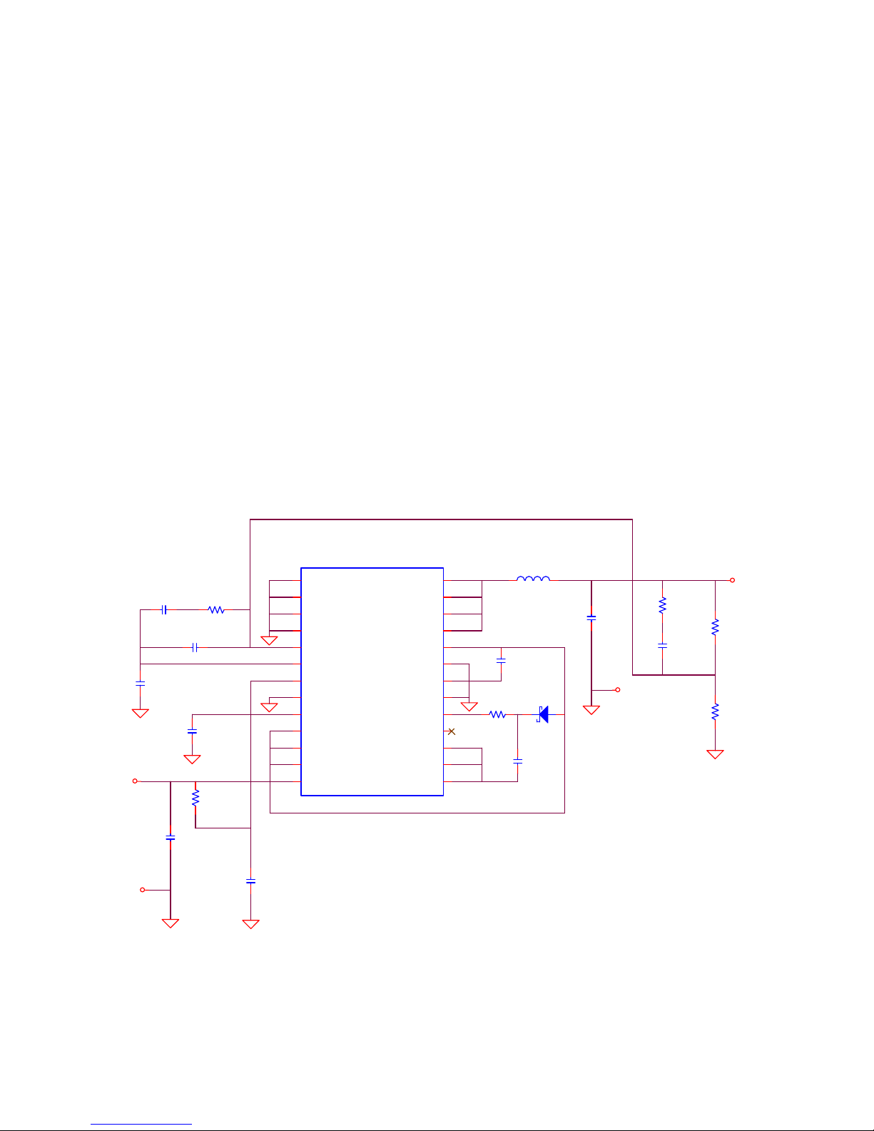
SP7650EB SCHEMATIC
CZ2
1,000pF
CF1
100pF
12V
VIN
C1
CERAMIC
1210
X5R
GND
RZ2
15k, 1%
CP1
22pF
fs=300Khz
C1
22uF
16V
CSS
47nF
R3
200k,1%
R4
100k,1%
C2
0.1uF
1
2
3
4
5
6
7
8
9
10
11
12
13
464,5%
1210
PGND
PGND
PGND
GND
VFB
COMP
UVIN
GND
SS
VIN
VIN
VIN
VIN
R6
U1
SP7650
LX
LX
LX
LX
VCC
GND
GND
GND
BST
NC
LX
LX
LX
D1
BZX384B5V6
Vz=5.6V
RBST
20
L1
6.8uH
CVCC
2.2uF
DBST
SD101AWS
CBST
6,800pF
C3
22uF
6.3V
GND2
C3
CERAMIC
1210
X5R
RZ3
7.15k ,1%
CZ3
150pF
VOUT
3.30V
0-3A
R1
68.1k ,1%
R2
21.5k,1%
26
25
24
23
22
21
20
19
18
17
16
15
14
Notes:
U1 Bottom-Side Layout should has
three Contacts which are
isolated from one of another, QT
& QB Drain Contact and
Controller GND Contact
All resistor & capacitor size
0603 unless other wise specify
Date: 01/04/05 SP7650 Evaluation BoardManual Copyright 2005 Sipex Corporation
Page 2

USING THE EVALUATION BOARD
1) Powering Up the SP7650EB Circuit
Connect the SP7650 Evaluation Board with an external +12V power supply. Connect
with short leads and large diameter wire directly to the “VIN” and “GND” posts. Connect
a Load between the VOUT and GND2 posts, again using short leads with large
diameter wire to minimize inductance and voltage drops.
2) Measuring Output Load Characteristics
It’s best to GND reference scope and digital meters using the Star GND post in the
center of the board. VOUT ripple can best be seen touching probe tip to the pad for C3
and scope GND collar touching Star GND post – avoid a GND lead on the scope which
will increase noise pickup.
3) Using the Evaluation Board with Different Output Voltages
While the SP7650 Evaluation Board has been tested and delivered with the output set
to 3.30V, by simply changing one resistor, R2, the SP7650 can be set to other output
voltages. The relationship in the following formula is based on a voltage divider from the
output to the feedback pin VFB, which is set to an internal reference voltage of 0.80V.
Standard 1% metal film resistors of surface mount size 0603 are recommended.
Vout = 0.80V ( R1 / R2 + 1 ) => R2 = R1 / [ ( Vout / 0.80V ) – 1 ]
Where R1 = 68.1KΩ and for Vout = 0.80V setting, simply remove R2 from the board.
Furthermore, one could select the value of R1 and R2 combination to meet the exact
output voltage setting by restricting R1 resistance range such that 50KΩ ≤ R1 ≤ 100KΩ
for overall system loop stability.
Note that since the SP7650 Evaluation Board design was optimized for 12V down
conversion to 3.30V, changes of output voltage and/or input voltage will alter
performance from the data given in the Power Supply Data section. In addition, the
SP7650ER provides short circuit protection by sensing Vout at GND.
POWER SUPPLY DATA
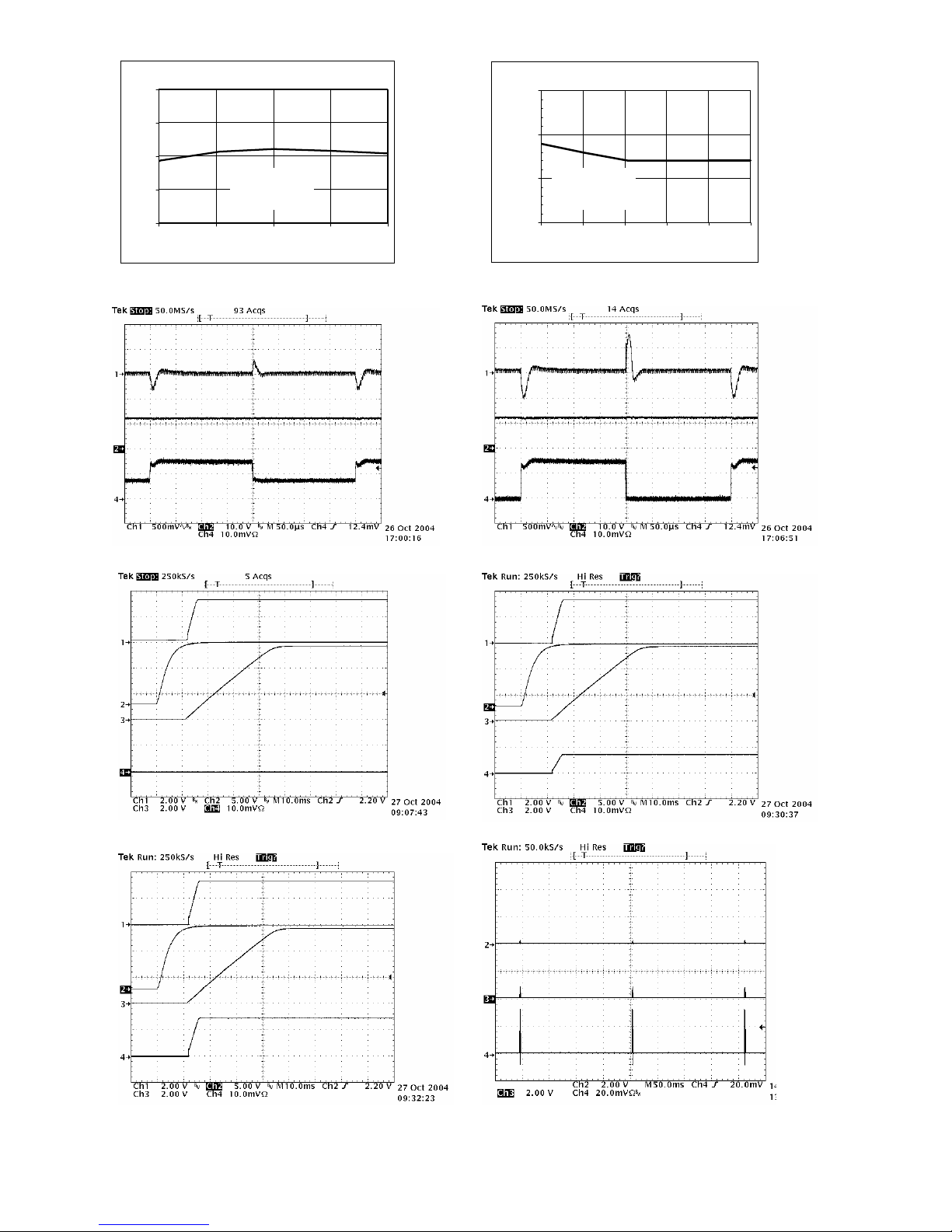
The SP7650ER is designed with a very accurate 1.0% reference over line, load and
temperature. Figure 1 data shows a typical SP7650 Evaluation Board Efficiency plot,
with efficiencies to 90% and output currents to 3A. SP7650ER Load Regulation is
shown in Figure 2 of only 0.1% change in output voltage from no load to 3A load.
Figures 3 and 4 illustrate a 1.5A to 3A and 0A to 3A Load Step. Start-up Response in
Figures 5, 6 and 7 show a controlled start-up with different output load behavior when
power is applied where the input current rises smoothly as the Softstart ramp increases.
In Figure 8 the SP7650ER is configured for hiccup mode in response to an output dead
short circuit condition and will Softstart until the over-load is removed. Figure 9 and 10
show output voltage ripple less than 40mV at no load to 3A load.
While data on individual power supply boards may vary, the capability of the SP7650ER
of achieving high accuracy over a range of load conditions shown here is quite
impressive and desirable for accurate power supply design.
2
Page 3
100
(
(
Efficiency vs Load
Load Regulation
3.305
95
90
85
Efficiency (%)
80
1.0 1.5 2.0 2.5 3.0
Vin=12V
Vout=3.3V
Load Current (A)
3.300
3.295
Output Voltage (V)
3.290
Vin=12V
Vout=3.3V
0.51.01.52.02.53.0
Load Current (A)
Figure 1. Efficiency vs Load Figure 2. Load Regulation
Vin
Iout (2A/div)
Vin
Iout (2A/div)
Vin=12V
Vout=3.3V
Vin=12V
Vout=3.3V
Figure 3. Load Step Response: 1.5->3A
Figure 4. Load Step Response: 0->3A
Vout
Vout
SoftStart
Vin
SoftStart
2A/div)
Iout
2A/div)
Iout
Figure 5. Start-Up Response: No Load
Figure 6. Start-Up Response: 1.5A Load
Vout
SoftStart
SoftStart
Vout
Iout (2A/div)
Ichoke (5A/div)
Figure 7. Start-Up Response: 3A Load Figure 8. Output Load Short Circuit
3
Page 4
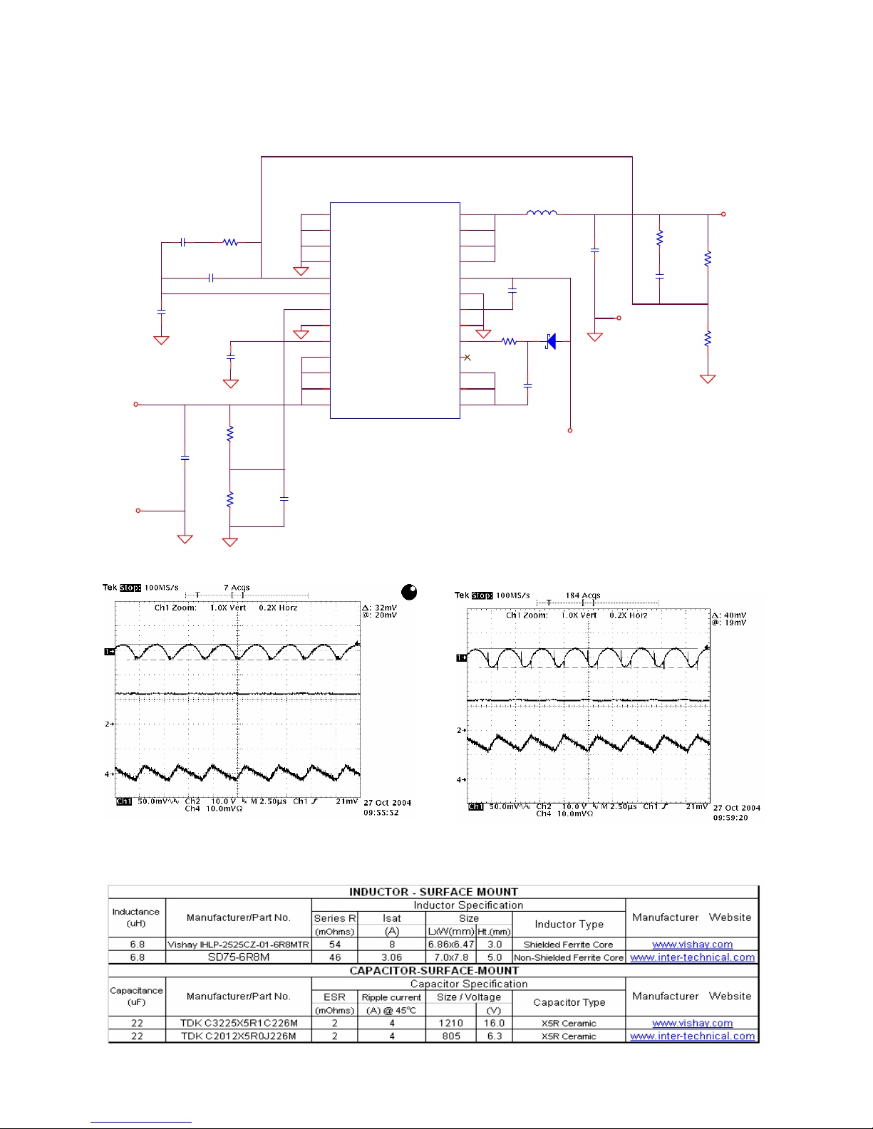
+5V BIAS SUPPLY APPLICATION SCHEMATIC
In this application example, the SP7650ER is power by an external +5V bias supply
which current consumption of 20mA Maximum. If this supply is not available than it is
recommend Sipex SPX5205 Low-Noise LDO Voltage Regulator.
U1
VIN
CF1
100pF
CZ2
1,000pF
fs=300Khz
CP1
22pF
RZ2
15k, 1%
47nF
SP7650
1
PGND
2
PGND
3
PGND
4
GND
5
VFB
6
COMP
7
UVIN
8
GND
9
SS
10
VIN
11
VIN
12
VIN
13
VIN
VCC
GND
GND
GND
BST
26
LX
25
LX
24
LX
23
LX
22
21
20
19
18
17
NC
16
LX
15
LX
14
LX
20
RBST
L1
6.8uH
CVCC
2.2uF
SD101AWS
DBS TCSS
CBST
6,800pF
C3
22uF
6.3V
GND2
C3
CERAMIC
1210
X5R
RZ3
7.15k ,1%
CZ3
150pF
VOUT
3.30V
0-3A
R1
68.1k,1%
R2
21.5k,1%
12V
GND
C1
CERAMIC
1210
X5R
C1
22uF
16V
R3
200k, 1%
R4
100k, 1%
Notes:
U1 Bottom-Side Layout should has
three Contacts which are
isolated from one of another, QT
& QB Drain Contact and
C2
Controller GND Contact
0.1uF
All resistor & capacitor size
0603 unless other wise specify
+5V
Vout ripple = 32mV
Figure 9. Output Ripple: No Load Figure 10. Output Ripple: 3A Load
Vout ripple = 40mV
Ichoke (2A/div)
Table 1: SP7650EB Suggested Components and Vendor Lists
4
Page 5
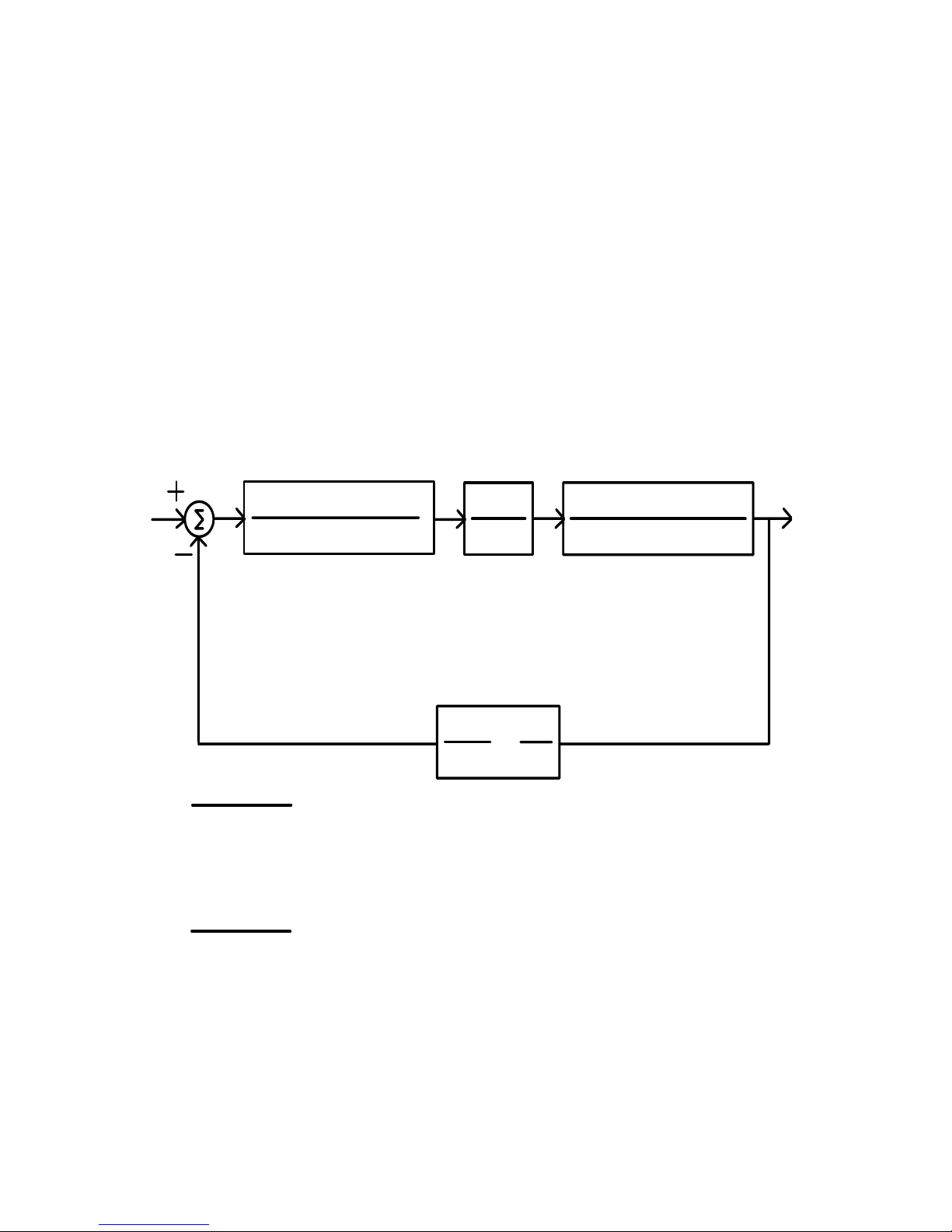
TYPE III LOOP COMPENSATION DESIGN
The open loop gain of the SP7650EB can be divided into the gain of the error amplifier
Gamp(s), PWM modulator Gpwm, buck converter output stage Gout(s), and feedback
resistor divider Gfbk. In order to crossover at the selecting frequency fco, the gain of
the error amplifier has to compensate for the attenuation caused by the rest of the loop
at this frequency. The goal of loop compensation is to manipulate the open loop
frequency response such that its gain crosses over 0dB at a slope of –20dB/dec. The
open loop crossover frequency should be higher than the ESR zero of the output
capacitors but less than 1/5 to 1/10 of the switching frequency fs to insure proper
operation. Since the SP7650EB is designed with Ceramic Type output capacitors, a
Type III compensation circuit is required to give a phase boost of 180° in order to
counteract the effects of the output LC under damped resonance double pole
frequency.
Type III Voltage Loop
Compensation Gamp(S)
Gain Block
PWM Stage
Gpwm
Output Stage
Gout(S)
Gain BlockGain Block
Vref
(Volts)
(SRz2Cz2+1)(SR1Cz3+1)
SR1Cz2(SRz3Cz3+1)(SRz2Cp1+1)
Vin
Vramp_pp
[S^2LCout+S(Resr+Rdc)Cout+1]
(SResrCout+1)
Voltage Feedback
Gfbk
Gain Block
Vfbk
R2
(R1+R2)
OR
Vref
Vout
(Volts)
Definitions:
Resr := Output Capacitor Equivalent Series Resitance
Rdc := Output Inductor DC Resistance
Vramp_pp := SP7650 Internal RAMP Amplitude Peak to Peak Voltage
Conditions:
Vout
(Volts)
Cz2 >> Cp1 and R1 >> Rz3
Output Load Resistance >> Resr and Rdc
Figure 11. Voltage Mode Control Loop with Loop Dynamic for Type III Compensation
The simple guidelines for positioning the poles and zeros and for calculating the
component values for Type III compensation are as follows:
5
Page 6

a. Choose fco = fs / 10
b. Calculate fp_LC
fp_LC = 1 / 2π [(L) (C)] ^ 1/2
c. Calculate fz_ESR
fz_ESR = 1 / 2π (Resr) (Cout)
d. Select R1 component value such that 50kΩ ≤ R1 ≤ 100kΩ
e. Calculate R2 base on the desired Vout
R2 = R1 / [(Vout / 0.80V) – 1]
f. Select the ratio of Rz2 / R1 gain for the desired gain bandwidth
Rz2 = R1 (Vramp_pp / Vin_max) (fco / fp_LC)
g. Calculate Cz2 by placing the zero at ½ of the output filter pole frequency
Cz2 = 1 / π (Rz2) (fp_LC)
h. Calculate Cp1 by placing the first pole at ESR zero frequency
Cp1 = 1 / 2π (Rz2) (fz_ESR)
i. Calculate Rz3 by setting the second pole at ½ of the switching frequency and the
second zero at the output filter double pole frequency
Rz3 = 2 (R1) (fp_LC) / fs
j. Calculate Cz3 from Rz3 component value above
Cz3 = 1 / π (Rz3) (fs)
k. Choose 100pF ≤ Cf1 ≤ 220pF to stabilize the SP7650ER internal Error Amplify
As a particular example, consider for the following SP7650EB with a Type III Voltage
Loop Compensation component selections:
Vin = 5 to 15V
Vout = 3.30V @ 0 to 3A load
Select L = 6.8uH => yield ≈ 40% of maximum 3A output current ripple.
Select Cout = 22uF Ceramic capacitor (Resr ≈ 4mΩ)
fs = 300khz SP7650 internal Oscillator Frequency
Vramp_pp = 1.0V SP7650 internal Ramp Peak to Peak Amplitude
Step by step design procedures:
a. fco = 300khz / 5 = 60khz
b. fp_LC = 1 / 2π [(6.8uH)(22uF)]^1/2 ≈ 15khz
c. fz_ESR = 1 / 2π (2mΩ)(22uF) ≈ 3.6Mhz
d. R1 = 68.1kΩ, 1%
6
Page 7
e. R2 = 68.1kΩ / [(3.30V / 0.80V) – 1] ≅ 21.5kΩ, 1%
f. Rz2 = 68.1kΩ (1.0V / 15V) (60khz / 15khz) ≈ 15kΩ, 1%
g. Cz2 = 1 / π (18kΩ) (20khz) ≈ 1,000pF, X7R
h. Cp1 = 1 / 2π (15kΩ) (3.6Mhz) ≈ 10pF => Select Cp1 = 22pF for noise filtering
i. Rz3 = 2 (68.1kΩ) (15khz) / 300khz ≈ 7.15kΩ, 1%
j. Cz3 = 1 / π (7.15kΩ) (300khz) ≅ 100pF, COG
k. Cf1 = 100pF to stabilize SP7650ER internal Error Amplify
+5V INPUT WITH A TYPE III COMPENSATION APPLICATION SCHEMATIC
Figure 12 shows another example of SP7650ER configures for +5V input by simply
changing a few external resistors and capacitors components value for delivering a 03A output with excellent line and load regulation.
U1
CF1
100pF
5V
VIN
C1
CERAMIC
0805
X5R
GND
CZ2
1,000pF
fs=300Khz
C1
22uF
6.3V
CP1
22pF
RZ2
15k,1%
47nF
R3
100k, 1%
C2
0.1uF
SP7650
1
PGND
2
PGND
3
PGND
4
GND
5
VFB
6
COMP
7
UVIN
8
GND
9
SS
10
VIN
11
VIN
12
VIN
13
VIN
VCC
GND
GND
GND
BST
NC
26
LX
25
LX
24
LX
23
LX
22
21
20
19
18
17
16
LX
15
LX
14
LX
Notes:
U1 Bottom-Side Layout should has
three Contacts which are
isolated from one of another, QT
& QB Drain Contact and
Controller GND Contact
All resistor & capacitor size
0603 unless other wise specify
RBST
CVCC
2.2uF
SD101AWS
20
L1
6.8uH
DBSTCSS
CBST
6,800pF
C3
22uF
6.3V
GND 2
C3
CERAMIC
1210
X5R
RZ3
7.15k,1%
CZ3
150pF
VOUT
3.30V
0-3A
R1
68.1k ,1%
R2
21.5k ,1%
Figure 12. SP7650ER Configures for Vin = 5V, Vout = 3.3V at 0-3A Output Load Current
7
Page 8
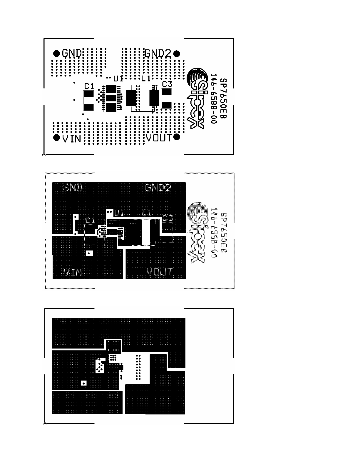
PC LAYOUT DRAWINGS
Figure 13. SP7650EB Component Placement
Figure 14. SP7650EB PC Layout Top Side
Figure 15. SP7650EB PC Layout 2nd Layer Side
8
Page 9
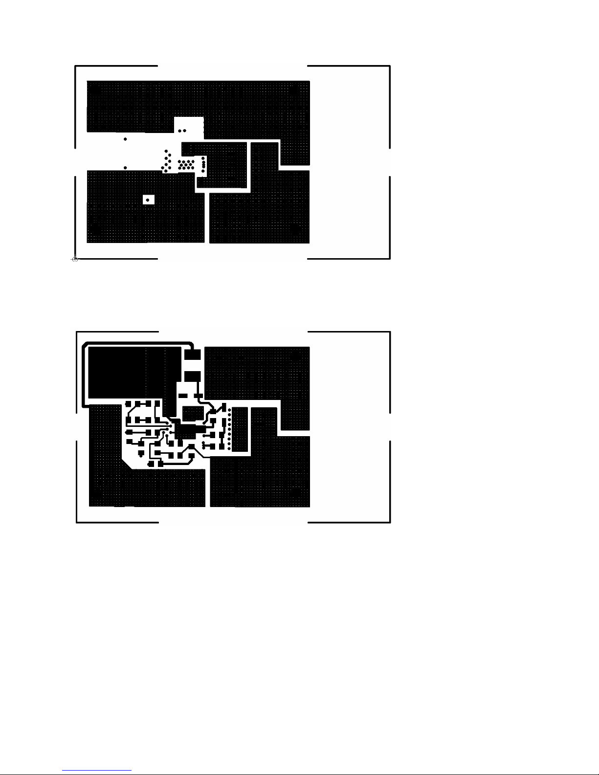
Figure 16. SP7650EB PC Layout 3rd Layer Side
Figure 17. SP7650EB PC Layout Bottom Side
9
Page 10
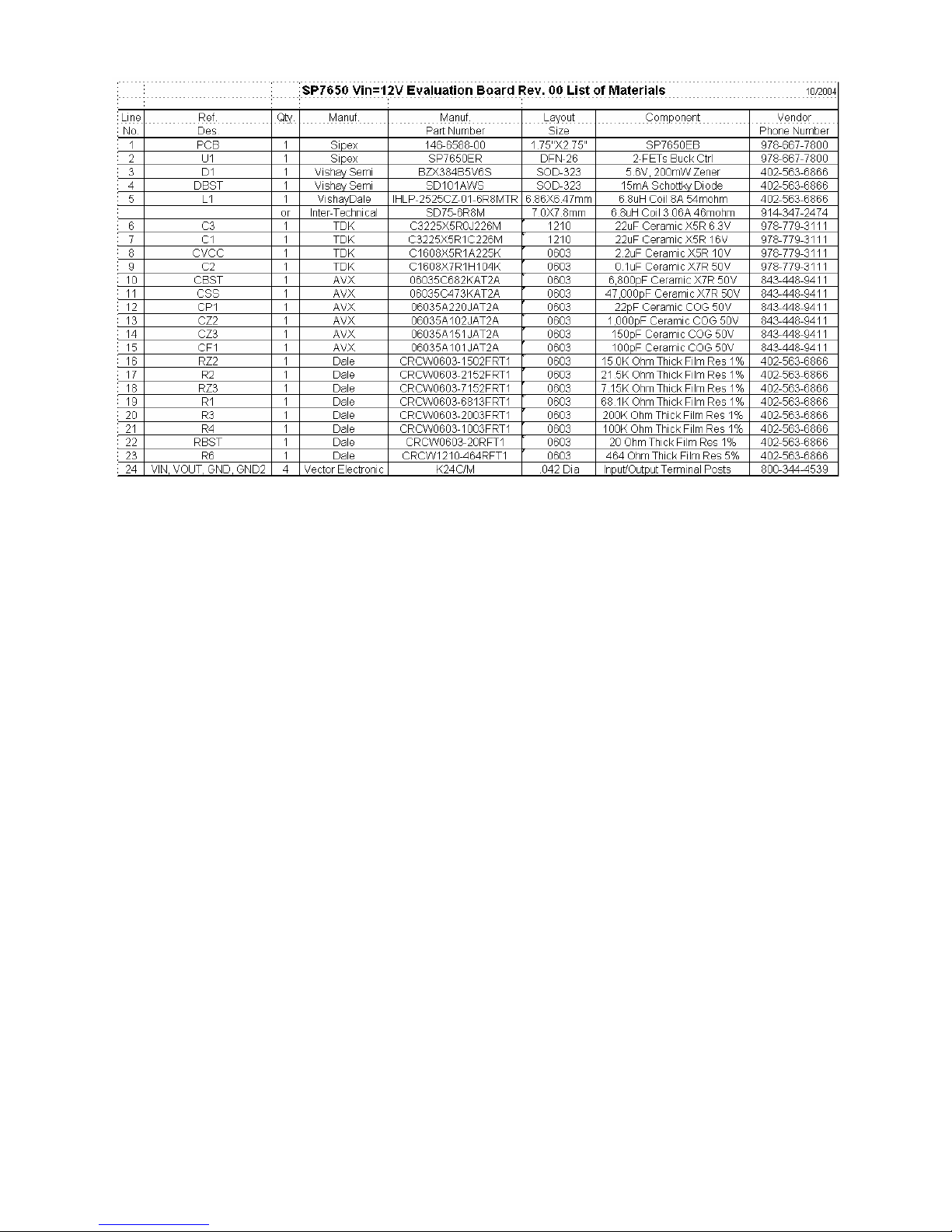
Table 2: SP7650EB List of Materials
8700
8700
-
-
ORDERING INFORMATION
Model Temperature Range Package Type
SP7650EB…................................-40°C to +85°C...............…SP7650 Evaluation Board
SP7650ER..............................…. -40°C to +85°C.................................……26-pin DFN
00
10
Page 11

Mouser Electronics
Authorized Distributor
Click to View Pricing, Inventory, Delivery & Lifecycle Information:
Exar:
SP7650EB
 Loading...